EP0472420B1 - Structure de connexion pour cartes à circuit intégré - Google Patents
Structure de connexion pour cartes à circuit intégré Download PDFInfo
- Publication number
- EP0472420B1 EP0472420B1 EP19910307690 EP91307690A EP0472420B1 EP 0472420 B1 EP0472420 B1 EP 0472420B1 EP 19910307690 EP19910307690 EP 19910307690 EP 91307690 A EP91307690 A EP 91307690A EP 0472420 B1 EP0472420 B1 EP 0472420B1
- Authority
- EP
- European Patent Office
- Prior art keywords
- card
- contact
- contact points
- connection structure
- terminals
- Prior art date
- Legal status (The legal status is an assumption and is not a legal conclusion. Google has not performed a legal analysis and makes no representation as to the accuracy of the status listed.)
- Expired - Lifetime
Links
Images


Classifications
-
- H—ELECTRICITY
- H05—ELECTRIC TECHNIQUES NOT OTHERWISE PROVIDED FOR
- H05K—PRINTED CIRCUITS; CASINGS OR CONSTRUCTIONAL DETAILS OF ELECTRIC APPARATUS; MANUFACTURE OF ASSEMBLAGES OF ELECTRICAL COMPONENTS
- H05K1/00—Printed circuits
- H05K1/02—Details
- H05K1/11—Printed elements for providing electric connections to or between printed circuits
- H05K1/118—Printed elements for providing electric connections to or between printed circuits specially for flexible printed circuits, e.g. using folded portions
-
- G—PHYSICS
- G06—COMPUTING; CALCULATING OR COUNTING
- G06K—GRAPHICAL DATA READING; PRESENTATION OF DATA; RECORD CARRIERS; HANDLING RECORD CARRIERS
- G06K19/00—Record carriers for use with machines and with at least a part designed to carry digital markings
- G06K19/06—Record carriers for use with machines and with at least a part designed to carry digital markings characterised by the kind of the digital marking, e.g. shape, nature, code
- G06K19/067—Record carriers with conductive marks, printed circuits or semiconductor circuit elements, e.g. credit or identity cards also with resonating or responding marks without active components
- G06K19/07—Record carriers with conductive marks, printed circuits or semiconductor circuit elements, e.g. credit or identity cards also with resonating or responding marks without active components with integrated circuit chips
- G06K19/077—Constructional details, e.g. mounting of circuits in the carrier
- G06K19/07737—Constructional details, e.g. mounting of circuits in the carrier the record carrier consisting of two or more mechanically separable parts
- G06K19/07741—Constructional details, e.g. mounting of circuits in the carrier the record carrier consisting of two or more mechanically separable parts comprising a first part operating as a regular record carrier and a second attachable part that changes the functional appearance of said record carrier, e.g. a contact-based smart card with an adapter part which, when attached to the contact card makes the contact card function as a non-contact card
-
- G—PHYSICS
- G06—COMPUTING; CALCULATING OR COUNTING
- G06K—GRAPHICAL DATA READING; PRESENTATION OF DATA; RECORD CARRIERS; HANDLING RECORD CARRIERS
- G06K7/00—Methods or arrangements for sensing record carriers, e.g. for reading patterns
- G06K7/0013—Methods or arrangements for sensing record carriers, e.g. for reading patterns by galvanic contacts, e.g. card connectors for ISO-7816 compliant smart cards or memory cards, e.g. SD card readers
- G06K7/0021—Methods or arrangements for sensing record carriers, e.g. for reading patterns by galvanic contacts, e.g. card connectors for ISO-7816 compliant smart cards or memory cards, e.g. SD card readers for reading/sensing record carriers having surface contacts
-
- H—ELECTRICITY
- H01—ELECTRIC ELEMENTS
- H01R—ELECTRICALLY-CONDUCTIVE CONNECTIONS; STRUCTURAL ASSOCIATIONS OF A PLURALITY OF MUTUALLY-INSULATED ELECTRICAL CONNECTING ELEMENTS; COUPLING DEVICES; CURRENT COLLECTORS
- H01R12/00—Structural associations of a plurality of mutually-insulated electrical connecting elements, specially adapted for printed circuits, e.g. printed circuit boards [PCB], flat or ribbon cables, or like generally planar structures, e.g. terminal strips, terminal blocks; Coupling devices specially adapted for printed circuits, flat or ribbon cables, or like generally planar structures; Terminals specially adapted for contact with, or insertion into, printed circuits, flat or ribbon cables, or like generally planar structures
- H01R12/50—Fixed connections
- H01R12/59—Fixed connections for flexible printed circuits, flat or ribbon cables or like structures
- H01R12/62—Fixed connections for flexible printed circuits, flat or ribbon cables or like structures connecting to rigid printed circuits or like structures
-
- H—ELECTRICITY
- H01—ELECTRIC ELEMENTS
- H01R—ELECTRICALLY-CONDUCTIVE CONNECTIONS; STRUCTURAL ASSOCIATIONS OF A PLURALITY OF MUTUALLY-INSULATED ELECTRICAL CONNECTING ELEMENTS; COUPLING DEVICES; CURRENT COLLECTORS
- H01R12/00—Structural associations of a plurality of mutually-insulated electrical connecting elements, specially adapted for printed circuits, e.g. printed circuit boards [PCB], flat or ribbon cables, or like generally planar structures, e.g. terminal strips, terminal blocks; Coupling devices specially adapted for printed circuits, flat or ribbon cables, or like generally planar structures; Terminals specially adapted for contact with, or insertion into, printed circuits, flat or ribbon cables, or like generally planar structures
- H01R12/70—Coupling devices
- H01R12/77—Coupling devices for flexible printed circuits, flat or ribbon cables or like structures
- H01R12/78—Coupling devices for flexible printed circuits, flat or ribbon cables or like structures connecting to other flexible printed circuits, flat or ribbon cables or like structures
-
- H—ELECTRICITY
- H05—ELECTRIC TECHNIQUES NOT OTHERWISE PROVIDED FOR
- H05K—PRINTED CIRCUITS; CASINGS OR CONSTRUCTIONAL DETAILS OF ELECTRIC APPARATUS; MANUFACTURE OF ASSEMBLAGES OF ELECTRICAL COMPONENTS
- H05K1/00—Printed circuits
- H05K1/02—Details
- H05K1/0286—Programmable, customizable or modifiable circuits
- H05K1/0295—Programmable, customizable or modifiable circuits adapted for choosing between different types or different locations of mounted components
-
- H—ELECTRICITY
- H05—ELECTRIC TECHNIQUES NOT OTHERWISE PROVIDED FOR
- H05K—PRINTED CIRCUITS; CASINGS OR CONSTRUCTIONAL DETAILS OF ELECTRIC APPARATUS; MANUFACTURE OF ASSEMBLAGES OF ELECTRICAL COMPONENTS
- H05K2201/00—Indexing scheme relating to printed circuits covered by H05K1/00
- H05K2201/09—Shape and layout
- H05K2201/09818—Shape or layout details not covered by a single group of H05K2201/09009 - H05K2201/09809
- H05K2201/09954—More mounting possibilities, e.g. on same place of PCB, or by using different sets of edge pads
-
- H—ELECTRICITY
- H05—ELECTRIC TECHNIQUES NOT OTHERWISE PROVIDED FOR
- H05K—PRINTED CIRCUITS; CASINGS OR CONSTRUCTIONAL DETAILS OF ELECTRIC APPARATUS; MANUFACTURE OF ASSEMBLAGES OF ELECTRICAL COMPONENTS
- H05K2201/00—Indexing scheme relating to printed circuits covered by H05K1/00
- H05K2201/10—Details of components or other objects attached to or integrated in a printed circuit board
- H05K2201/10007—Types of components
- H05K2201/10189—Non-printed connector
-
- H—ELECTRICITY
- H05—ELECTRIC TECHNIQUES NOT OTHERWISE PROVIDED FOR
- H05K—PRINTED CIRCUITS; CASINGS OR CONSTRUCTIONAL DETAILS OF ELECTRIC APPARATUS; MANUFACTURE OF ASSEMBLAGES OF ELECTRICAL COMPONENTS
- H05K3/00—Apparatus or processes for manufacturing printed circuits
- H05K3/30—Assembling printed circuits with electric components, e.g. with resistor
- H05K3/32—Assembling printed circuits with electric components, e.g. with resistor electrically connecting electric components or wires to printed circuits
- H05K3/34—Assembling printed circuits with electric components, e.g. with resistor electrically connecting electric components or wires to printed circuits by soldering
- H05K3/3447—Lead-in-hole components
Definitions
- the present invention relates to an IC card connection structure for connecting an IC card reader or writer to an IC card, including contact points arranged to contact the electrical terminals of an IC card.
- IC cards There are two types of IC cards as an international standard (standard stipulated in 7816-2 of International Organization for Standardization), i.e. an upper position type and a lower position type depending on the difference of the arrangement of the IC contact positions.
- JP-A-01-226090 An IC card connection structure for connecting an IC card reader or writer to an IC card, including contact points arranged to contact the electrical terminals of an IC card is disclosed in JP-A-01-226090.
- this document discloses the structure as having a sliding contact which is slidable relative to an upper position or a lower position of the IC contact positions on the IC card so as to contact the contact points in the upper position or the lower position.
- an operator usually judges that the IC contact position of the IC card is the upper position type or the lower position type and thereafter slides the contact.
- a connection strucure according to the present invention characterised in that the contact points include a first group of contact points include a first group of contact points disposed for contacting IC card terminals configured in a first manner on the card and a second group of contact points disposed for contacting IC card terminals configured in a second, different manner on the card.
- the contact pins on the contact for enabling the contact with the contact points of the IC card in common with the two types of contact positions.
- it is possible to obviate the occurrence of sliding of the contact in the wrong or intermediate position so as to assure the supply and reception of the data between the IC card and the IC card reader/writer and eliminate the breakage of the IC chip.
- the IC card connection structure will be described with reference to Figs.1 to 8.
- Fig. 5 is a perspective view of a typical IC card transaction processing apparatus 11.
- the IC card transaction processing apparatus 11 comprises a key board 12 for receiving data, a display 13 for displaying the operation guide of the apparatus 11 and the input data, a printing portion 14 for printing a transaction detail on a roll sheet and an IC card insertion portion 15.
- Fig. 6 is an enlarged perspective view showing the IC card insertion portion 15 in Fig. 5.
- the IC card insertion portion 15 comprises an IC card insertion slit 16 in which an IC card having contact points 17 for contacting the IC contact is inserted.
- 18 is a contact for contacting the contact points 17 of the IC card, thereby suppying data to or receiving data from the IC card reader/writer, not shown.
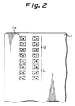
- Fig. 2 is a plan view showing an arrangement of the contact points 1a of the IC card 1, wherein the contact points 1a are located at a position U, if the IC contact position is the upper position type, while the contacts 1a are located at a position L, if the IC contact position is the lower position type.
- contact points 1a in both the upper and lower position types are denoted by the same numerals C1 to C8.
- C1 are circuit voltage terminals
- C2 are reset signal terminals
- C3 are program supply voltage terminals
- C4 are spare terminals
- C5 are zero voltage terminals
- C6 program supply voltage terminals
- C7 data input/output terminals
- C8 are spare terminals.
- Fig. 1 is a perspective view showing the IC card connection structure according to the present invention.
- Denoted at 1 is the IC card
- 3 is a control circuit of the IC card reader/writer
- 4 is a contact.
- the contact 4 has contact pins 5 at upper and lower surfaces thereof for contacting all the contact points 1a arranged in both the upper contact position U and the lower contact position L.
- 6 is a flexible cable for connecting the contact 4 to the control circuit 3 and has soldered portions 8 which the contact pins 5 are inserted into and connected to.
- 7 is a connector mounted on the control circuit 3 for inserting the flexible cable 6 thereinto.
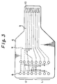
- Fig. 3 is a plan view of the flexible cable 6.
- the flexible cable has the soldered portion 8 at one end portion thereof as set forth above and leads 9 made of copper foil which are provided at the upper and lower surfaces thereof and connected to the soldered portion 8 located at the side of the upper contact position U and the side of the lower contact position L.
- the flexible cable further has contact portions 10 provided at the other end portion thereof for connecting the soldered portions 8 located at the side of the upper position U to the corresponding solderd portion 8 located at the side of the lower position L.
- Fig. 4 is a plan view of a flexible cable according to a modification of the present invention.
- the copper leads 9 are provided at one side surface of the flexible cable 6.
- the flexible cable 6 is not limited to those as illustrated in Fig. 3 and 4 but may be those capable of connecting the soldered portions located at the side of the upper position U to the corresponding soldered portions located at the side of the lower position L.
- the contact pins 5 of the contact 4 can contact the contact points 1a in either case where the contact points are located at the upper position U or the lower position L.
- the signals transmitted from the IC card 1 to the contact 4 by way of the contact points 1a located at the upper position U or the lower position L are supplied to the contact portions 10 by way of the leads 9, then supplied to the control circuit 3.
- Fig. 7 is a plan view showing an arrangement of contact points 31a of an IC card according to another modification of the present invention.
- Fig. 8 is a plan view of a flexible cable which is used when the IC card 21 in Fig. 7 is employed.
- the flexible cable comprises soldered portions 28 provided at one end thereof which contact pins of a contact are inserted into and connected to, and leads 29 made of copper foil and provided at an upper surface thereof and connected to the soldered portions 28 located at the side of the upper position and the corresponding soldered portions 28 located at the side of the lower position.
- the flexible cable further comprises contact portions 30 provided at the other end thereof for connecting the soldered portions 28, located at the side of the upper position, and the corresponding soldered portions 28, located at the side of the lower position, for supplying the signals issued from the IC card by way of the contact points in the upper position, or the corresponding contact points in the lower position, to an IC card reader/writer.
- the leads 29 are not provided on both surfaces of the flexible cable 26 but on one surface thereof, and it is possible to obviate the need to provide leads 29 between each soldered portion 28 on both sides of the flexible cable.
- the IC card connection structure With the arrangement of the IC card connection structure, it is possible to coneect the IC card to the control circuit of the IC card reader/writer in either case where the IC card has the upper position type or the lower position type.
Landscapes
- Engineering & Computer Science (AREA)
- Microelectronics & Electronic Packaging (AREA)
- Physics & Mathematics (AREA)
- General Physics & Mathematics (AREA)
- Theoretical Computer Science (AREA)
- Artificial Intelligence (AREA)
- Computer Vision & Pattern Recognition (AREA)
- Computer Hardware Design (AREA)
- Coupling Device And Connection With Printed Circuit (AREA)
- Multi-Conductor Connections (AREA)
- Credit Cards Or The Like (AREA)
Claims (5)
- Structure de connexion de carte à circuit imprimé pour connecter un lecteur ou enregistreur sur carte à circuit imprimé à une carte à circuit imprimé, comprenant des pointes de contact (5) disposées de façon à entrer en contact avec les bornes électriques (1a, 31c) d'une carte (1) à circuit imprimé, caractérisée en ce que lesdites pointes (5) de contact comprennent un premier groupe de pointes de contact disposées pour entrer en contact avec des bornes d'une carte à circuit imprimé configurées d'une première maniyre (U) sur la carte et un second groupe de pointes de contact disposées pour entrer en contact avec des bornes d'une carte à circuit imprimé configurées d'une seconde manière différente (L) sur la carte.
- Structure de connexion selon la revendication 1, dans laquelle il y a au moins 16 points (5) de contact.
- Structure de connexion selon la revendication 1 ou 2, dans laquelle les pointes (5) de contact sont montées dans un support commun (4).
- Structure de connexion selon la revendication 3, comprenant un élément (6, 26) de connexion à une extrémité duquel le support commun (4) est monté, l'élément (6, 28) de connexion étant poourvu de bornes (8, 28) pour entrer en contact avec les pointes (5) de contact, de parties (10, 30) de contact à une extrémité éloignée des bornes (8, 28) et de pistes conductrices couplant chaque partie (10, 30) de contact à une pointe de contact respective (5) dans chacun desdits groupes (U, L).
- Structure de connexion selon la revendication 4, dans laquelle l'élément (6, 28) de connexion est un câble flexible.
Applications Claiming Priority (2)
| Application Number | Priority Date | Filing Date | Title |
|---|---|---|---|
| JP218996/90 | 1990-08-22 | ||
| JP2218996A JP2726329B2 (ja) | 1990-08-22 | 1990-08-22 | Icカードリーダライタのicカード接続構造 |
Publications (3)
| Publication Number | Publication Date |
|---|---|
| EP0472420A2 EP0472420A2 (fr) | 1992-02-26 |
| EP0472420A3 EP0472420A3 (en) | 1992-11-19 |
| EP0472420B1 true EP0472420B1 (fr) | 1995-11-22 |
Family
ID=16728633
Family Applications (1)
| Application Number | Title | Priority Date | Filing Date |
|---|---|---|---|
| EP19910307690 Expired - Lifetime EP0472420B1 (fr) | 1990-08-22 | 1991-08-21 | Structure de connexion pour cartes à circuit intégré |
Country Status (3)
| Country | Link |
|---|---|
| EP (1) | EP0472420B1 (fr) |
| JP (1) | JP2726329B2 (fr) |
| DE (1) | DE69114784T2 (fr) |
Families Citing this family (3)
| Publication number | Priority date | Publication date | Assignee | Title |
|---|---|---|---|---|
| DE4417088C2 (de) * | 1993-05-14 | 2001-11-29 | Amphenol Tuchel Elect | Kontaktiersystem für Chipkarten |
| DE4326029C2 (de) * | 1993-08-03 | 1995-05-24 | Amphenol Tuchel Elect | Leser für Informationskarten |
| JP5896577B2 (ja) * | 2011-12-14 | 2016-03-30 | デューラ−ヴェルケ・ドゥストマン・ウント・コンパニー・ゲゼルシャフト・ミト・ベシュレンクテル・ハフツング | 負荷に電気エネルギーを供給する装置及びそのためのシステム |
Family Cites Families (4)
| Publication number | Priority date | Publication date | Assignee | Title |
|---|---|---|---|---|
| DE3235212A1 (de) * | 1982-09-23 | 1984-03-29 | Schoeller & Co Elektronik Gmbh, 3552 Wetter | Kontaktierungselement fuer gedruckte schaltungen |
| FR2607291B1 (fr) * | 1986-11-21 | 1991-04-19 | Flonic Sa | Ensemble de connexion pour cartes a memoire electronique et dispositif de lecture/ecriture en faisant application |
| JPH01226090A (ja) * | 1988-03-07 | 1989-09-08 | Sharp Corp | Icカードリーダーライター |
| EP0357827A1 (fr) * | 1988-09-09 | 1990-03-14 | Sixcom S.P.A. | Lecteur multifonctionnel pour cartes à bande magnétique, cartes à code à barres optiques, cartes à microprocesseur électronique, comportant une source de lumière et un détecteur à haute résolution pour des rayons réfléchis par la carte |
-
1990
- 1990-08-22 JP JP2218996A patent/JP2726329B2/ja not_active Expired - Lifetime
-
1991
- 1991-08-21 EP EP19910307690 patent/EP0472420B1/fr not_active Expired - Lifetime
- 1991-08-21 DE DE1991614784 patent/DE69114784T2/de not_active Expired - Fee Related
Also Published As
| Publication number | Publication date |
|---|---|
| EP0472420A2 (fr) | 1992-02-26 |
| EP0472420A3 (en) | 1992-11-19 |
| JP2726329B2 (ja) | 1998-03-11 |
| JPH04102184A (ja) | 1992-04-03 |
| DE69114784T2 (de) | 1996-06-05 |
| DE69114784D1 (de) | 1996-01-04 |
Similar Documents
| Publication | Publication Date | Title |
|---|---|---|
| US7364436B2 (en) | Low height USB interface connecting device and a memory storage apparatus thereof | |
| US20040117515A1 (en) | Distributing system | |
| EP0195159B1 (fr) | Carte portative à circuits intégrés semi-conducteurs | |
| EP1192581A1 (fr) | Lecteur de carte a puce | |
| KR19990067235A (ko) | 스마트 카드 및 스마트 카드 커넥터 | |
| MY111915A (en) | Printed circuit card with minor surface i/o pads. | |
| US5924881A (en) | Electrical connector for IC card | |
| US6050857A (en) | SIM connector and related contact | |
| MY122287A (en) | Smart card reader for elevated placement relative to a printed circuit board | |
| EP0472420B1 (fr) | Structure de connexion pour cartes à circuit intégré | |
| EP0926617B1 (fr) | Lecteur de cartes à puce | |
| EP1333531A1 (fr) | Connecteur à hauteur réduite pour une interface USB et unité de mémoire correspondante | |
| US5554840A (en) | Hybrid card reader | |
| ATE67327T1 (de) | Kartenleser. | |
| EP0773607A3 (fr) | Connecteur de bord de carte | |
| JPH03194680A (ja) | メモリカード用アダプタ | |
| KR100516907B1 (ko) | 낮은 프로파일의 usb인터페이스 연결장치 및 메모리저장장치 | |
| EP1427062B1 (fr) | Connecteur electrique | |
| JPH0935031A (ja) | 接触ユニット用の接点部 | |
| US6508673B2 (en) | Low cost smart card reader, extension style, with wiping contacts | |
| US20060084321A1 (en) | Small-size connector enabling selective use of different types of connection objects | |
| JPH01226090A (ja) | Icカードリーダーライター | |
| JPH06337735A (ja) | Icカード型入出力装置、ケーブルコネクタ及び端末機 | |
| EP0840541A1 (fr) | Carte vidéo | |
| JPH06216550A (ja) | プリント基板接続装置 |
Legal Events
| Date | Code | Title | Description |
|---|---|---|---|
| PUAI | Public reference made under article 153(3) epc to a published international application that has entered the european phase |
Free format text: ORIGINAL CODE: 0009012 |
|
| AK | Designated contracting states |
Kind code of ref document: A2 Designated state(s): DE FR GB NL |
|
| PUAL | Search report despatched |
Free format text: ORIGINAL CODE: 0009013 |
|
| AK | Designated contracting states |
Kind code of ref document: A3 Designated state(s): DE FR GB NL |
|
| 17P | Request for examination filed |
Effective date: 19921218 |
|
| 17Q | First examination report despatched |
Effective date: 19940620 |
|
| GRAA | (expected) grant |
Free format text: ORIGINAL CODE: 0009210 |
|
| AK | Designated contracting states |
Kind code of ref document: B1 Designated state(s): DE FR GB NL |
|
| REF | Corresponds to: |
Ref document number: 69114784 Country of ref document: DE Date of ref document: 19960104 |
|
| ET | Fr: translation filed | ||
| PLBE | No opposition filed within time limit |
Free format text: ORIGINAL CODE: 0009261 |
|
| STAA | Information on the status of an ep patent application or granted ep patent |
Free format text: STATUS: NO OPPOSITION FILED WITHIN TIME LIMIT |
|
| 26N | No opposition filed | ||
| PGFP | Annual fee paid to national office [announced via postgrant information from national office to epo] |
Ref country code: GB Payment date: 19980812 Year of fee payment: 8 |
|
| PGFP | Annual fee paid to national office [announced via postgrant information from national office to epo] |
Ref country code: FR Payment date: 19980814 Year of fee payment: 8 |
|
| PGFP | Annual fee paid to national office [announced via postgrant information from national office to epo] |
Ref country code: NL Payment date: 19980827 Year of fee payment: 8 |
|
| PGFP | Annual fee paid to national office [announced via postgrant information from national office to epo] |
Ref country code: DE Payment date: 19980831 Year of fee payment: 8 |
|
| PG25 | Lapsed in a contracting state [announced via postgrant information from national office to epo] |
Ref country code: GB Free format text: LAPSE BECAUSE OF NON-PAYMENT OF DUE FEES Effective date: 19990821 |
|
| PG25 | Lapsed in a contracting state [announced via postgrant information from national office to epo] |
Ref country code: NL Free format text: LAPSE BECAUSE OF NON-PAYMENT OF DUE FEES Effective date: 20000301 |
|
| GBPC | Gb: european patent ceased through non-payment of renewal fee |
Effective date: 19990821 |
|
| PG25 | Lapsed in a contracting state [announced via postgrant information from national office to epo] |
Ref country code: FR Free format text: LAPSE BECAUSE OF NON-PAYMENT OF DUE FEES Effective date: 20000428 |
|
| NLV4 | Nl: lapsed or anulled due to non-payment of the annual fee |
Effective date: 20000301 |
|
| PG25 | Lapsed in a contracting state [announced via postgrant information from national office to epo] |
Ref country code: DE Free format text: LAPSE BECAUSE OF NON-PAYMENT OF DUE FEES Effective date: 20000601 |
|
| REG | Reference to a national code |
Ref country code: FR Ref legal event code: ST |