EP0469605B1 - Verfahren um die Verschlechterung der Eigenschaften eines Halbleiterlasers zu verringern - Google Patents
Verfahren um die Verschlechterung der Eigenschaften eines Halbleiterlasers zu verringern Download PDFInfo
- Publication number
- EP0469605B1 EP0469605B1 EP91112951A EP91112951A EP0469605B1 EP 0469605 B1 EP0469605 B1 EP 0469605B1 EP 91112951 A EP91112951 A EP 91112951A EP 91112951 A EP91112951 A EP 91112951A EP 0469605 B1 EP0469605 B1 EP 0469605B1
- Authority
- EP
- European Patent Office
- Prior art keywords
- sulfur
- side surfaces
- semiconductor laser
- resonator
- passivation
- Prior art date
- Legal status (The legal status is an assumption and is not a legal conclusion. Google has not performed a legal analysis and makes no representation as to the accuracy of the status listed.)
- Expired - Lifetime
Links
- 239000004065 semiconductor Substances 0.000 title claims description 18
- 238000000034 method Methods 0.000 title claims description 14
- 230000015556 catabolic process Effects 0.000 title description 10
- 238000006731 degradation reaction Methods 0.000 title description 10
- NINIDFKCEFEMDL-UHFFFAOYSA-N Sulfur Chemical compound [S] NINIDFKCEFEMDL-UHFFFAOYSA-N 0.000 claims description 22
- 229910052717 sulfur Inorganic materials 0.000 claims description 22
- 239000011593 sulfur Substances 0.000 claims description 22
- 238000002161 passivation Methods 0.000 claims description 19
- NBIIXXVUZAFLBC-UHFFFAOYSA-N Phosphoric acid Chemical compound OP(O)(O)=O NBIIXXVUZAFLBC-UHFFFAOYSA-N 0.000 claims description 17
- VYPSYNLAJGMNEJ-UHFFFAOYSA-N Silicium dioxide Chemical compound O=[Si]=O VYPSYNLAJGMNEJ-UHFFFAOYSA-N 0.000 claims description 8
- 229910000147 aluminium phosphate Inorganic materials 0.000 claims description 8
- 238000005530 etching Methods 0.000 claims description 3
- 229910052814 silicon oxide Inorganic materials 0.000 claims description 3
- 229910052733 gallium Inorganic materials 0.000 claims description 2
- 229910052581 Si3N4 Inorganic materials 0.000 claims 1
- NCMAYWHYXSWFGB-UHFFFAOYSA-N [Si].[N+][O-] Chemical compound [Si].[N+][O-] NCMAYWHYXSWFGB-UHFFFAOYSA-N 0.000 claims 1
- UYJXRRSPUVSSMN-UHFFFAOYSA-P ammonium sulfide Chemical compound [NH4+].[NH4+].[S-2] UYJXRRSPUVSSMN-UHFFFAOYSA-P 0.000 claims 1
- HQVNEWCFYHHQES-UHFFFAOYSA-N silicon nitride Chemical compound N12[Si]34N5[Si]62N3[Si]51N64 HQVNEWCFYHHQES-UHFFFAOYSA-N 0.000 claims 1
- 230000000694 effects Effects 0.000 description 13
- 238000003776 cleavage reaction Methods 0.000 description 10
- 238000005424 photoluminescence Methods 0.000 description 10
- 230000007017 scission Effects 0.000 description 10
- 238000011282 treatment Methods 0.000 description 10
- 239000013078 crystal Substances 0.000 description 7
- BUGBHKTXTAQXES-UHFFFAOYSA-N Selenium Chemical compound [Se] BUGBHKTXTAQXES-UHFFFAOYSA-N 0.000 description 6
- 229910052711 selenium Inorganic materials 0.000 description 6
- 239000011669 selenium Substances 0.000 description 6
- 229910000980 Aluminium gallium arsenide Inorganic materials 0.000 description 3
- 230000015572 biosynthetic process Effects 0.000 description 3
- 238000006243 chemical reaction Methods 0.000 description 3
- 229910052681 coesite Inorganic materials 0.000 description 3
- 229910052906 cristobalite Inorganic materials 0.000 description 3
- 239000000377 silicon dioxide Substances 0.000 description 3
- 238000004544 sputter deposition Methods 0.000 description 3
- 229910052682 stishovite Inorganic materials 0.000 description 3
- 239000000758 substrate Substances 0.000 description 3
- 229910052905 tridymite Inorganic materials 0.000 description 3
- QAOWNCQODCNURD-UHFFFAOYSA-N Sulfuric acid Chemical compound OS(O)(=O)=O QAOWNCQODCNURD-UHFFFAOYSA-N 0.000 description 2
- 239000000463 material Substances 0.000 description 2
- 238000012986 modification Methods 0.000 description 2
- 230000004048 modification Effects 0.000 description 2
- 238000005268 plasma chemical vapour deposition Methods 0.000 description 2
- 230000002265 prevention Effects 0.000 description 2
- 239000002344 surface layer Substances 0.000 description 2
- 229910001218 Gallium arsenide Inorganic materials 0.000 description 1
- 229910004205 SiNX Inorganic materials 0.000 description 1
- BLRPTPMANUNPDV-UHFFFAOYSA-N Silane Chemical compound [SiH4] BLRPTPMANUNPDV-UHFFFAOYSA-N 0.000 description 1
- 239000007789 gas Substances 0.000 description 1
- 125000005842 heteroatom Chemical group 0.000 description 1
- 150000002500 ions Chemical class 0.000 description 1
- 239000002184 metal Substances 0.000 description 1
- 229910052751 metal Inorganic materials 0.000 description 1
- 150000005837 radical ions Chemical class 0.000 description 1
- 238000005215 recombination Methods 0.000 description 1
- 230000006798 recombination Effects 0.000 description 1
- 239000007787 solid Substances 0.000 description 1
- 239000000126 substance Substances 0.000 description 1
Images

Classifications
-
- H—ELECTRICITY
- H01—ELECTRIC ELEMENTS
- H01S—DEVICES USING THE PROCESS OF LIGHT AMPLIFICATION BY STIMULATED EMISSION OF RADIATION [LASER] TO AMPLIFY OR GENERATE LIGHT; DEVICES USING STIMULATED EMISSION OF ELECTROMAGNETIC RADIATION IN WAVE RANGES OTHER THAN OPTICAL
- H01S5/00—Semiconductor lasers
- H01S5/02—Structural details or components not essential to laser action
- H01S5/028—Coatings ; Treatment of the laser facets, e.g. etching, passivation layers or reflecting layers
-
- H—ELECTRICITY
- H01—ELECTRIC ELEMENTS
- H01S—DEVICES USING THE PROCESS OF LIGHT AMPLIFICATION BY STIMULATED EMISSION OF RADIATION [LASER] TO AMPLIFY OR GENERATE LIGHT; DEVICES USING STIMULATED EMISSION OF ELECTROMAGNETIC RADIATION IN WAVE RANGES OTHER THAN OPTICAL
- H01S5/00—Semiconductor lasers
- H01S5/30—Structure or shape of the active region; Materials used for the active region
- H01S5/32—Structure or shape of the active region; Materials used for the active region comprising PN junctions, e.g. hetero- or double- heterostructures
-
- H—ELECTRICITY
- H01—ELECTRIC ELEMENTS
- H01S—DEVICES USING THE PROCESS OF LIGHT AMPLIFICATION BY STIMULATED EMISSION OF RADIATION [LASER] TO AMPLIFY OR GENERATE LIGHT; DEVICES USING STIMULATED EMISSION OF ELECTROMAGNETIC RADIATION IN WAVE RANGES OTHER THAN OPTICAL
- H01S5/00—Semiconductor lasers
- H01S5/02—Structural details or components not essential to laser action
- H01S5/028—Coatings ; Treatment of the laser facets, e.g. etching, passivation layers or reflecting layers
- H01S5/0282—Passivation layers or treatments
Definitions
- This invention relates to a process for reducing characteristics degradation of a semiconductor laser and comprises the protection of the side surfaces of the resonator thereof.
- a known major factor for the degradation of the characteristics of a semiconductor laser is degradation of the side surfaces of the resonator.
- Prior art for the prevention of such degradation are described, e.g., in Japanese Patent Publication Nos. 37828/1987, 34835/1985 and 43910/1988.
- "Effects of (NH 4 ) 2 S Treatments on the Characteristics of AlGaAs Laser Diodes” (Extended Abstract of the 21st Conference on Solids Devices and Materials, Tokyo, 1989, pp. 337-340) describes the art for preventing the degradation of the side surfaces of the resonator of a semiconductor laser by reducing the interface states by sulfur passivation.
- the inventors found the fact that the sulfur passivated side surfaces of a resonator are very sensitive to the following protection film forming process, and ECR-CVD can suppress the degradation of the effect of the sulfur-passivation.
- the process for forming a protection film for a semiconductor laser this invention relates to is characterized in that the side surfaces of the semiconductor laser are sulfur-passivated, and subsequently a protection film is formed by ECR-CVD.
- ECR-CVD the reaction chamber is divided in a plasma generating chamber and a film forming chamber, and the plasma does not damage the side surfaces of a resonator. Resultantly the effect of the sulfur passivation is not degraded.
- the side surfaces of a resonator may be treated with a phosphoric acid-based etchant, whereby the protection effect of the side surfaces of the resonator can be more improved.
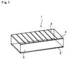
- FIG. 1 is a perspective view of a semiconductor laser the process according to this invention is applicable to.
- a rod-shaped laser crystal 1 is cloven to form the side surfaces of a resonator.
- An n-electrode 2 is formed on the bottom surface, and stripe regions 3 and p-electrodes 4 are alternately formed on the top surface.
- the laser crystal 1 has AlGaAs double hetero-structure but may have AlInGaP/GaAs structure, InGaAsP/InP structure or others.
- a cleavage plane 5 (a side surface of a resonator) of the laser crystal 1 is sulfur-passivated by sulfur reaction.
- the cleavage plane 5 is immersed in a solution of (NH 4 ) 2 S or (NH 4 ) 2 S X (1 ⁇ x ⁇ 3) to terminate dangling bonds in the cleavage plane 5.
- the cleavage plane 5 may be treated with a phosphoric acid-based etchant prior to the sulfur passivation. The latter treatment prevents the natural formation of an oxide film, and is suitable for the case that a protection film is not immediately formed on the cleavage plane 5. Subsequently a protection film is formed by ECR-CVD.
- the laser crystal 1 of FIG. 1 is cloven in the longitudinal direction of the stripe regions 3.
- a desired semiconductor laser device is fabricated.
- Samples were prepared as follows. First a laser crystal of AlGaAs double hetero junction-structure was prepared. A Ti/Pt/Au p type-electrode was formed on the surface on the side of the p type-semiconductor crystal, and an AuGe/Ni/Au n type-electrode was formed on the surface on the side of the n-semiconductor. This rod-shaped crystal was cloven on both sides to form side surfaces of a resonator. The thus-prepared samples were subjected to the treatments of Example 1, and Comparisons 1 and 2 which will be described below.
- a sample was immersed in a solution of (NH 4 ) 2 S X for 10 minutes and then water-cleaned. Then the sample held by a jig was placed in the film forming chamber of an ECR-CVD apparatus so that a film is formed on the cleavage plane, and a SiN film was formed using SiH 4 and N 2 gases. At this time, the p type- and n type-electrode forming portions were covered with metal films attached to jigs so that the SiN film is not formed on the p type-electrode and the n type-electrode.
- the radical ion shower from the plasma generating chamber to the film forming chamber has such a high directivity that few ions turn in. Consequently the resultant semiconductor laser has few recombinations on the side surfaces of the resonator and little natural oxide film.
- the cleavage plane of a sample was sulfur-passivated by the same process as in Example 1. Then the sample was set in a sputtering apparatus, and a SiO 2 film was formed on the cleave plane.
- Laser diodes using the thus-treated samples were compared first in laser beam output.
- the laser diode of Example 1 exhibited an output 1.5 times that of Comparison 1, and 3 times that of Comparison 2.
- the laser diodes were compared.
- the laser diode of Example 1 exhibited a lifetime 4 times that of Comparison 1 and 20 time that of Comparison 2.
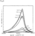
- FIG. 2 The result of this comparison is shown in FIG. 2.
- Curve (a) in FIG. 2 shows the photoluminescence of the case in which the sulfur passivation was followed by the formation of a silicon oxide protection film. A high photoluminescence intensity was obtained at the band edge.
- Curve (b) shows the photoluminescence intensity of the case where the sulfur-passivation was performed, but no protection film was formed.
- Curve (c) shows the photoluminescence intensity of the case where the film was formed by sputtering
- Curve (d) shows that of the case where the film was formed by pyrolytic CVD. It is found that the effect of the sulfur passivation in these cases is degraded in comparison with that of ECR-CVD.
- Curve (e) shows the photoluminescence intensity of the film formed by the plasma CVD at RF of 13.56 MHz.
- Curve (g) shows the photoluminescence of the film formed by the plasma CVD at RF of 50 KHz. It is seen that the effect of the sulfur passivation is much reduced.
- Curve (d) shows the photoluminescence of the case where none of the treatments were made.
- FIG. 3 The result of this comparison is shown in FIG. 3.
- the isotropic etchant means etchants which form etched surfaces in inversed and normal mesas, and phosphoric acid-based etchants form etched surfaces in generally normal mesas and are called here isotropic etchants.
- sulfur passivation treatment is applied to a surface of the semiconductor substrate after etching with a phosphoric acid-based etchant.
- selenium is one element in VI group in which sulfur is included and has chemical properties similar to that of sulfur.
- atomic radius of selenium is nearer to those of Ga and As than that of sulfur and therefore it is possible that the selenium surface layer has lower energy level than that of sulfur surface layer and as the result is more stable than that of sulfur. See Journal of Applied Physics Vol. 67 No. 1, 1 January 1990, pages 586 to 588, "Enhanced electronic properties of GaAs surface chemically passivated by selenium reactions".
- the passivation treatment using selenium can be applied to the surface of the semiconductor substrate instead of the sulfur passivation treatment of the above embodiment and the advantageous effect in the surface states density which is obtained by the sulfur passivation may be also obtained by the selenium passivation.
- ECR-CVD is used to form a passivated protection film. Consequently side surfaces of the resonators which are little degraded and have good reflection characteristics can be realized. Furthermore, the effects can be further improved by the treatment with isotropic etchants, such as phosphoric acid-based etchants.
Landscapes
- Physics & Mathematics (AREA)
- Condensed Matter Physics & Semiconductors (AREA)
- General Physics & Mathematics (AREA)
- Electromagnetism (AREA)
- Optics & Photonics (AREA)
- Semiconductor Lasers (AREA)
Claims (4)
- Ein Verfahren zum Ausbilden einer Schutzschicht auf einem Ga und As enthaltenden Halbleiterlaser, das die Schritte aufweist:Ätzen von Seitenflächen eines Resonators des Halbleiterlasers mit einem auf Phosphorsäure basierenden Ätzmittel; Schwefel-Passivierung der geätzten Seitenflächen nach dem Ätzschritt; undAusbilden einer Schutzschicht auf den Schwefelpassivierten Seitenflächen mittels Elektronen-Zyklotron-Resonanz-CVD nach dem Schwefel-Passivierungsschritt.
- Ein Verfahren nach Anspruch 1,
wobei die Schwefel-Passivierung durch Eintauchen der Resonatorseitenflächen in ein Ammoniumsulfit durchgeführt wird, das übermäßig Schwefel enthält. - Ein Verfahren nach einem vorhergehenden Anspruch,
wobei die Schutzschicht aus Siliciumoxid, Siliciumnitrid oder Silicium-Stickstoff-Oxid hergestellt wird. - Ein Verfahren nach einem vorhergehenden Anspruch, das den Schritt der Selen-Passivierung der Seitenflächen anstelle von deren Schwefel-Passivierung aufweist.
Applications Claiming Priority (2)
| Application Number | Priority Date | Filing Date | Title |
|---|---|---|---|
| JP2204527A JP2841775B2 (ja) | 1990-08-01 | 1990-08-01 | 半導体レーザの保護膜形成方法 |
| JP204527/90 | 1990-08-01 |
Publications (3)
| Publication Number | Publication Date |
|---|---|
| EP0469605A2 EP0469605A2 (de) | 1992-02-05 |
| EP0469605A3 EP0469605A3 (en) | 1992-09-02 |
| EP0469605B1 true EP0469605B1 (de) | 1996-06-12 |
Family
ID=16492013
Family Applications (1)
| Application Number | Title | Priority Date | Filing Date |
|---|---|---|---|
| EP91112951A Expired - Lifetime EP0469605B1 (de) | 1990-08-01 | 1991-08-01 | Verfahren um die Verschlechterung der Eigenschaften eines Halbleiterlasers zu verringern |
Country Status (5)
| Country | Link |
|---|---|
| EP (1) | EP0469605B1 (de) |
| JP (1) | JP2841775B2 (de) |
| KR (1) | KR950004598B1 (de) |
| CA (1) | CA2048205A1 (de) |
| DE (1) | DE69120159D1 (de) |
Families Citing this family (2)
| Publication number | Priority date | Publication date | Assignee | Title |
|---|---|---|---|---|
| US5393680A (en) * | 1990-08-01 | 1995-02-28 | Sumitomo Electric Industries, Ltd. | MIS electrode forming process |
| KR100730767B1 (ko) * | 2001-12-06 | 2007-06-21 | 코오롱생명과학 주식회사 | 디벤조티에핀 유도체의 신규 제조방법 |
-
1990
- 1990-08-01 JP JP2204527A patent/JP2841775B2/ja not_active Expired - Lifetime
-
1991
- 1991-07-31 CA CA002048205A patent/CA2048205A1/en not_active Abandoned
- 1991-07-31 KR KR1019910013192A patent/KR950004598B1/ko not_active Expired - Fee Related
- 1991-08-01 EP EP91112951A patent/EP0469605B1/de not_active Expired - Lifetime
- 1991-08-01 DE DE69120159T patent/DE69120159D1/de not_active Expired - Lifetime
Also Published As
| Publication number | Publication date |
|---|---|
| KR920005417A (ko) | 1992-03-28 |
| DE69120159D1 (de) | 1996-07-18 |
| EP0469605A2 (de) | 1992-02-05 |
| JP2841775B2 (ja) | 1998-12-24 |
| KR950004598B1 (ko) | 1995-05-02 |
| CA2048205A1 (en) | 1992-02-02 |
| EP0469605A3 (en) | 1992-09-02 |
| JPH0488691A (ja) | 1992-03-23 |
Similar Documents
| Publication | Publication Date | Title |
|---|---|---|
| US6803605B2 (en) | Method to GaAs based lasers and a GaAs based laser | |
| US6067310A (en) | Semiconductor laser and method of making the same | |
| US6653663B2 (en) | Nitride semiconductor device | |
| US4987096A (en) | Manufacturing method of semiconductor laser with non-absorbing mirror structure | |
| CA1151775A (en) | Batch processing of semiconductor devices | |
| US10103517B2 (en) | High reliability etched-facet photonic devices | |
| EP0666603A2 (de) | Obere Abdeckschichtstruktur für lichtemittierendes Bauelement und Herstellungsverfahren. | |
| EP0469604A2 (de) | Verfahren zum Herstellen einer MIS-Elektrode | |
| US6665325B2 (en) | Quantum cascade laser and method for making same | |
| US4121179A (en) | Semiconductor injection laser | |
| US6914923B2 (en) | Semiconductor laser and manufacturing method thereof | |
| US5838028A (en) | Semiconductor device having a ridge or groove | |
| US4766472A (en) | Monolithic semiconductor structure of a laser and a field effect transistor | |
| EP0757393A2 (de) | Lichtemittierende Halbleitervorrichtung und Herstellungsverfahren | |
| EP0469605A2 (de) | Verfahren um die Verschlechterung der Eigenschaften eines Halbleiterlasers zu verringern | |
| US5770525A (en) | Method of fabricating semiconductor device and method of fabricating high-frequency semiconductor device | |
| US5181218A (en) | Manufacturing method of semiconductor laser with non-absorbing mirror structure | |
| US4689115A (en) | Gaseous etching process | |
| EP0469606A2 (de) | Verfahren zum Herstellen einer MES-Elektrode | |
| US5010375A (en) | Semiconductor laser device | |
| US5478437A (en) | Selective processing using a hydrocarbon and hydrogen | |
| Frateschi et al. | InGaAs/GaAs quantum well lasers with dry‐etched mirror passivated by vacuum atomic layer epitaxy | |
| KR950001145B1 (ko) | 헤테로접합 쌍극성 트랜지스터의 제조방법 | |
| JPH09205254A (ja) | 半導体装置の製造方法および半導体製造装置並びに半導体レーザの製造方法 | |
| Vermaerke et al. | Fast and reliable processing of high-performance InGaAs 0.98-um laser diodes |
Legal Events
| Date | Code | Title | Description |
|---|---|---|---|
| PUAI | Public reference made under article 153(3) epc to a published international application that has entered the european phase |
Free format text: ORIGINAL CODE: 0009012 |
|
| AK | Designated contracting states |
Kind code of ref document: A2 Designated state(s): DE FR GB NL |
|
| PUAL | Search report despatched |
Free format text: ORIGINAL CODE: 0009013 |
|
| AK | Designated contracting states |
Kind code of ref document: A3 Designated state(s): DE FR GB NL |
|
| 17P | Request for examination filed |
Effective date: 19930302 |
|
| 17Q | First examination report despatched |
Effective date: 19931116 |
|
| GRAH | Despatch of communication of intention to grant a patent |
Free format text: ORIGINAL CODE: EPIDOS IGRA |
|
| GRAA | (expected) grant |
Free format text: ORIGINAL CODE: 0009210 |
|
| AK | Designated contracting states |
Kind code of ref document: B1 Designated state(s): DE FR GB NL |
|
| REF | Corresponds to: |
Ref document number: 69120159 Country of ref document: DE Date of ref document: 19960718 |
|
| PG25 | Lapsed in a contracting state [announced via postgrant information from national office to epo] |
Ref country code: DE Effective date: 19960913 |
|
| ET | Fr: translation filed | ||
| PLBE | No opposition filed within time limit |
Free format text: ORIGINAL CODE: 0009261 |
|
| STAA | Information on the status of an ep patent application or granted ep patent |
Free format text: STATUS: NO OPPOSITION FILED WITHIN TIME LIMIT |
|
| 26N | No opposition filed | ||
| PGFP | Annual fee paid to national office [announced via postgrant information from national office to epo] |
Ref country code: GB Payment date: 19980723 Year of fee payment: 8 |
|
| PGFP | Annual fee paid to national office [announced via postgrant information from national office to epo] |
Ref country code: FR Payment date: 19980814 Year of fee payment: 8 |
|
| PGFP | Annual fee paid to national office [announced via postgrant information from national office to epo] |
Ref country code: NL Payment date: 19980827 Year of fee payment: 8 |
|
| PG25 | Lapsed in a contracting state [announced via postgrant information from national office to epo] |
Ref country code: GB Free format text: LAPSE BECAUSE OF NON-PAYMENT OF DUE FEES Effective date: 19990801 |
|
| PG25 | Lapsed in a contracting state [announced via postgrant information from national office to epo] |
Ref country code: NL Free format text: LAPSE BECAUSE OF NON-PAYMENT OF DUE FEES Effective date: 20000301 |
|
| GBPC | Gb: european patent ceased through non-payment of renewal fee |
Effective date: 19990801 |
|
| PG25 | Lapsed in a contracting state [announced via postgrant information from national office to epo] |
Ref country code: FR Free format text: LAPSE BECAUSE OF NON-PAYMENT OF DUE FEES Effective date: 20000428 |
|
| NLV4 | Nl: lapsed or anulled due to non-payment of the annual fee |
Effective date: 20000301 |
|
| REG | Reference to a national code |
Ref country code: FR Ref legal event code: ST |