EP0469565A2 - Apparatus for reading and/or inputting information - Google Patents
Apparatus for reading and/or inputting information Download PDFInfo
- Publication number
- EP0469565A2 EP0469565A2 EP91112832A EP91112832A EP0469565A2 EP 0469565 A2 EP0469565 A2 EP 0469565A2 EP 91112832 A EP91112832 A EP 91112832A EP 91112832 A EP91112832 A EP 91112832A EP 0469565 A2 EP0469565 A2 EP 0469565A2
- Authority
- EP
- European Patent Office
- Prior art keywords
- voltage
- information
- information medium
- probe electrode
- voltage application
- Prior art date
- Legal status (The legal status is an assumption and is not a legal conclusion. Google has not performed a legal analysis and makes no representation as to the accuracy of the status listed.)
- Granted
Links
- 239000000523 sample Substances 0.000 claims abstract description 125
- 238000000034 method Methods 0.000 claims abstract description 30
- 230000008569 process Effects 0.000 claims abstract description 10
- 230000007246 mechanism Effects 0.000 claims description 20
- 230000010354 integration Effects 0.000 claims description 15
- 239000010409 thin film Substances 0.000 claims description 11
- 239000002245 particle Substances 0.000 claims description 4
- 230000001678 irradiating effect Effects 0.000 claims 2
- 230000000694 effects Effects 0.000 abstract description 13
- 230000002411 adverse Effects 0.000 abstract description 4
- 230000008021 deposition Effects 0.000 abstract 1
- 230000008859 change Effects 0.000 description 25
- 239000000758 substrate Substances 0.000 description 19
- 239000000463 material Substances 0.000 description 8
- 230000015654 memory Effects 0.000 description 8
- 230000003446 memory effect Effects 0.000 description 8
- 238000001514 detection method Methods 0.000 description 6
- 239000010408 film Substances 0.000 description 5
- 238000010521 absorption reaction Methods 0.000 description 3
- 230000008901 benefit Effects 0.000 description 3
- 230000015556 catabolic process Effects 0.000 description 3
- 238000006731 degradation reaction Methods 0.000 description 3
- 238000009825 accumulation Methods 0.000 description 2
- 239000000470 constituent Substances 0.000 description 2
- 238000000354 decomposition reaction Methods 0.000 description 2
- 230000006866 deterioration Effects 0.000 description 2
- 238000007599 discharging Methods 0.000 description 2
- 230000005684 electric field Effects 0.000 description 2
- PCHJSUWPFVWCPO-UHFFFAOYSA-N gold Chemical compound [Au] PCHJSUWPFVWCPO-UHFFFAOYSA-N 0.000 description 2
- 239000010931 gold Substances 0.000 description 2
- 229910052737 gold Inorganic materials 0.000 description 2
- 239000004065 semiconductor Substances 0.000 description 2
- 239000000126 substance Substances 0.000 description 2
- 239000000725 suspension Substances 0.000 description 2
- 230000003466 anti-cipated effect Effects 0.000 description 1
- 150000001786 chalcogen compounds Chemical class 0.000 description 1
- 238000004040 coloring Methods 0.000 description 1
- 239000004020 conductor Substances 0.000 description 1
- 238000007796 conventional method Methods 0.000 description 1
- 230000003247 decreasing effect Effects 0.000 description 1
- 238000010894 electron beam technology Methods 0.000 description 1
- 238000005516 engineering process Methods 0.000 description 1
- 238000010884 ion-beam technique Methods 0.000 description 1
- 230000003287 optical effect Effects 0.000 description 1
- 150000002894 organic compounds Chemical class 0.000 description 1
- 230000002093 peripheral effect Effects 0.000 description 1
- 230000007480 spreading Effects 0.000 description 1
- 238000003892 spreading Methods 0.000 description 1
Images


Classifications
-
- B—PERFORMING OPERATIONS; TRANSPORTING
- B82—NANOTECHNOLOGY
- B82Y—SPECIFIC USES OR APPLICATIONS OF NANOSTRUCTURES; MEASUREMENT OR ANALYSIS OF NANOSTRUCTURES; MANUFACTURE OR TREATMENT OF NANOSTRUCTURES
- B82Y15/00—Nanotechnology for interacting, sensing or actuating, e.g. quantum dots as markers in protein assays or molecular motors
-
- G—PHYSICS
- G11—INFORMATION STORAGE
- G11B—INFORMATION STORAGE BASED ON RELATIVE MOVEMENT BETWEEN RECORD CARRIER AND TRANSDUCER
- G11B9/00—Recording or reproducing using a method not covered by one of the main groups G11B3/00 - G11B7/00; Record carriers therefor
- G11B9/12—Recording or reproducing using a method not covered by one of the main groups G11B3/00 - G11B7/00; Record carriers therefor using near-field interactions; Record carriers therefor
- G11B9/14—Recording or reproducing using a method not covered by one of the main groups G11B3/00 - G11B7/00; Record carriers therefor using near-field interactions; Record carriers therefor using microscopic probe means, i.e. recording or reproducing by means directly associated with the tip of a microscopic electrical probe as used in Scanning Tunneling Microscopy [STM] or Atomic Force Microscopy [AFM] for inducing physical or electrical perturbations in a recording medium; Record carriers or media specially adapted for such transducing of information
-
- B—PERFORMING OPERATIONS; TRANSPORTING
- B82—NANOTECHNOLOGY
- B82Y—SPECIFIC USES OR APPLICATIONS OF NANOSTRUCTURES; MEASUREMENT OR ANALYSIS OF NANOSTRUCTURES; MANUFACTURE OR TREATMENT OF NANOSTRUCTURES
- B82Y10/00—Nanotechnology for information processing, storage or transmission, e.g. quantum computing or single electron logic
-
- G—PHYSICS
- G11—INFORMATION STORAGE
- G11B—INFORMATION STORAGE BASED ON RELATIVE MOVEMENT BETWEEN RECORD CARRIER AND TRANSDUCER
- G11B11/00—Recording on or reproducing from the same record carrier wherein for these two operations the methods are covered by different main groups of groups G11B3/00 - G11B7/00 or by different subgroups of group G11B9/00; Record carriers therefor
- G11B11/002—Recording on or reproducing from the same record carrier wherein for these two operations the methods are covered by different main groups of groups G11B3/00 - G11B7/00 or by different subgroups of group G11B9/00; Record carriers therefor using recording by perturbation of the physical or electrical structure
-
- G—PHYSICS
- G11—INFORMATION STORAGE
- G11B—INFORMATION STORAGE BASED ON RELATIVE MOVEMENT BETWEEN RECORD CARRIER AND TRANSDUCER
- G11B19/00—Driving, starting, stopping record carriers not specifically of filamentary or web form, or of supports therefor; Control thereof; Control of operating function ; Driving both disc and head
- G11B19/02—Control of operating function, e.g. switching from recording to reproducing
- G11B19/04—Arrangements for preventing, inhibiting, or warning against double recording on the same blank or against other recording or reproducing malfunctions
-
- G—PHYSICS
- G11—INFORMATION STORAGE
- G11B—INFORMATION STORAGE BASED ON RELATIVE MOVEMENT BETWEEN RECORD CARRIER AND TRANSDUCER
- G11B23/00—Record carriers not specific to the method of recording or reproducing; Accessories, e.g. containers, specially adapted for co-operation with the recording or reproducing apparatus ; Intermediate mediums; Apparatus or processes specially adapted for their manufacture
- G11B23/50—Reconditioning of record carriers; Cleaning of record carriers ; Carrying-off electrostatic charges
-
- Y—GENERAL TAGGING OF NEW TECHNOLOGICAL DEVELOPMENTS; GENERAL TAGGING OF CROSS-SECTIONAL TECHNOLOGIES SPANNING OVER SEVERAL SECTIONS OF THE IPC; TECHNICAL SUBJECTS COVERED BY FORMER USPC CROSS-REFERENCE ART COLLECTIONS [XRACs] AND DIGESTS
- Y10—TECHNICAL SUBJECTS COVERED BY FORMER USPC
- Y10S—TECHNICAL SUBJECTS COVERED BY FORMER USPC CROSS-REFERENCE ART COLLECTIONS [XRACs] AND DIGESTS
- Y10S977/00—Nanotechnology
- Y10S977/84—Manufacture, treatment, or detection of nanostructure
- Y10S977/849—Manufacture, treatment, or detection of nanostructure with scanning probe
- Y10S977/86—Scanning probe structure
- Y10S977/868—Scanning probe structure with optical means
-
- Y—GENERAL TAGGING OF NEW TECHNOLOGICAL DEVELOPMENTS; GENERAL TAGGING OF CROSS-SECTIONAL TECHNOLOGIES SPANNING OVER SEVERAL SECTIONS OF THE IPC; TECHNICAL SUBJECTS COVERED BY FORMER USPC CROSS-REFERENCE ART COLLECTIONS [XRACs] AND DIGESTS
- Y10—TECHNICAL SUBJECTS COVERED BY FORMER USPC
- Y10S—TECHNICAL SUBJECTS COVERED BY FORMER USPC CROSS-REFERENCE ART COLLECTIONS [XRACs] AND DIGESTS
- Y10S977/00—Nanotechnology
- Y10S977/902—Specified use of nanostructure
- Y10S977/932—Specified use of nanostructure for electronic or optoelectronic application
- Y10S977/943—Information storage or retrieval using nanostructure
- Y10S977/947—Information storage or retrieval using nanostructure with scanning probe instrument
Definitions
- the present invention relates to an apparatus for reading and/or inputting information and a method therefor. More particularly, the present invention relates to an apparatus for reading and/or inputting information and a method therefor by applying a voltage to a recording medium when information is read or inputted.
- the present information is particularly suited for a recording and reproducing apparatus utilizing the principle of the scanning tunnel microscope (STM).
- STM scanning tunnel microscope
- STM scanning tunnel microscope
- the STM utilizes the fact that when a metallic probe (probe electrode) and a conductive substance approach to each together up to a distance of approximately 1 nm while a voltage is being applied therebetween, a tunnel current flows. This current is quite sensitive to the difference in the distances between them. Therefore, it is possible to draw the surface structure in a real space by enabling the probe to scan so that a constant tunnel current is maintained, and at the same time to read various information concerning the entire electron cloud. At this juncture, the resolution in the direction toward the inner surface is approximately 1 ⁇ . Accordingly, by applying the principle of the STM it is possible to perform a high-resolution recording and reproducing with an atomic order (several ⁇ ) satisfactorily.
- the recording and reproducing are performed in an area of an extremely narrow molecular order as compared with the conventional systems. Therefore, even an extremely small absorption of molecule to the surface of the recording medium, which should be negligible in the usual floppy disc type magnetic or optomagnetic recording and reproducing apparatus, or an extremely slight degradation or decomposition of the film quality, may cause a failure in writing or an error in reading.
- a first object of the present invention is to provide an apparatus for reading and inputting of information with medium having said electric memory effect by applying voltage in which the absorption of molecule, the degradation and decomposition of the medium and the like are eliminated, thus preventing the errors in reading and in putting information.
- Fig. 1 is a view showing the structure of the recording and reproducing apparatus of a first embodiment according to the present invention.
- a numeral 10 designates a probe electrode; 22, a substrate electrode; and 21, a recording medium having the electric memory effect, which is sandwiched between the probe electrode 10 and substrate electrode 22.
- the substrate electrode 22 and recording medium 21 are formed integrally on a substrate 23.
- a numeral 15 designates a voltage application means to apply a voltage between the probe 10 and substrate electrode 22, and generate a voltage V B .
- a numeral 17 designates a current detection means to detect a current flowing between the probe electrode 10 and recording medium 21; 12, a Z-direction fine traveling control mechanism to cause the probe electrode 10 to be traveled in the Z direction finely; 16, a servo circuit to control the distance (Z direction) between the probe electrode 10 and recording medium 21 using the Z-direction fine traveling control mechanism 12 on the basis of the current detection means 17.
- the servo circuit 16, current detection means 17, and Z-direction fine traveling mechanism 12 constitute a part of a space controlling means to control the distance between the probe 10 and recording medium 21.
- a numeral 201 designates a primary current-voltage converter having a sufficiently small inner resistance y as compared with the resistance between the probe electrode 10 and substrate electrode 22, which outputs the detected current value after having converted it into a sufficiently large voltage signal corresponding thereto.
- a numeral 202 designates a converter for converting the voltage signal containing the signed (positive or negative) current (J T ) received from the current-voltage converter 201 to a signal corresponding to a logarithmic value log I JT of the absolute value of the J T , and the output therefrom is transmitted to a differential divider 203.
- the differential divider 203 outputs the difference between a signal 206 and a signal corresponding to the log
- This differential signal is transmitted to a frequency filter 204 thereby to cut the high-frequency signal corresponding to the recording information.
- a numeral 205 designates an amplifier circuit for amplifying a signal which has passed through the filter 204.
- the signal passed through the amplifier circuit 205 becomes an information signal having an averaged space (averaged space of an area sufficiently larger than the recording bit) between the recording medium 21 and probe 10, which is transmitted to a microcomputer 19. Then, on the basis of this information signal, the microcomputer 19 transmits an instruction signal to the servo circuit 16 so as to make the averaged space between the probe electrode 10 and recording medium 21 constant.
- a part of the output of the converter 202 is directly transmitted to the microcomputer 19 through a frequency filter 207 which passes a high-frequency signal and cuts a low frequency signal such as corresponding to the averaged space information between the probe electrode 10 and recording medium 21. At the time of information reproducing, this signal becomes the recording information signal, which is processed by the microcomputer 19 to reproduce.
- a numeral 11 designates an x-y direction fine traveling control mechanism for driving finely the probe electrode 10 and fine traveling control mechanism 12 in the x-y direction to cause the probe electrode 10 to travel finely along the surface of the recording medium 21.
- Numerals 13, 14 designate a y-axial scanning driver and an x-axial scanning driver for applying a y-direction driving control voltage Vy and an x-direction driving control voltage V x to the x-y direction fine traveling control mechanism 11, respectively.
- the x-y direction fine traveling control mechanism 11 causes the probe electrode 10 to be displaced in the x-y directions in accordance with the voltage value applied respectively by the drivers 13 and 14.
- a numeral 24 designates an x-y stage to enable the substrate 23 to travel in the X-Y directions roughly; 25, a rough traveling mechanism to cause the x-y stage 24 to travel in the Z direction roughly; 18, a rough traveling driver to transmit controlling signals to the x-y stage 24 and rough traveling mechanism 25 in accordance with the instruction signals from the microcomputer 19; and 26, a support base.
- Fig. 2A and Fig. 2B illustrate the changes per time t in the x and y direction driving control voltages V x and Vy and the applied voltage V B by the voltage application means 15 at the time of information recording, i.e., the output states of the drivers 13 and 14 which have received instruction from the microcomputer 19 and the means 15 as well as the manner in which the recording is performed at that time.
- FIG. 2A shows the waveforms per time of the Y-axial driving control voltage Vy applied to the x-y direction fine traveling control mechanism 11 which causes the probe electrode 10 to travel along the surface of the recording medium 21; the middle stage thereof, the waveforms per time of the driving control voltage V x in the X axial direction applied to the x-y fine traveling control mechanism 11; and the lower stage thereof, the waveforms per time of the voltage applied between the probe 10 and substrate electrode 22.
- Fig. 2A is a time chart of the applied voltage at the time of recording
- Fig. 2B is a view schematically showing the manner in which information is written onto the recording medium according to the time chart shown in Fig. 2A as an example.
- the tip of the probe electrode 10 travels along arrows sequentially over the positions represented by 0 on the recording medium 21 as shown in Fig. 2B.
- the traveling of the probe electrode 10 is substantially instantaneous, and the probe electrode 10 stops at the positions represented by 0 for a predetermined period of time.
- this predetermined period of time is shown by numerals 31 to 40 per each position represented by mark 0 , and also in each of the positions marked 0 , the position at which a predetermined voltage is applied to generate a change in the recording medium 21, is represented by slanted lines in 0 in Fig. 2B.
- the broken line 41 shows the upper potential level (zero level) of the recording medium 21, and the broken line 42 shows the threshold potential which causes the recording medium 21 at the phase level indicated by the broken line 41 to change (shifting to the on-state), respectively.
- each of the recording bit positions, i.e. in each of the periods 31 - 40, the value of time integration [f V B (t) dt], of the applied voltage V B (voltage between the medium 21 and probe electrode 10) to the recording medium is substantially zero. In other words, the averaged value of V B in each of the periods becomes substantially zero.
- the absolute value of the applied voltage V B should be equalized at half point in each of the periods to inverse plus and minus.
- the absolute value of the applied voltage V B at this time should be the value suited for detecting the tunnel current J T in order to control the average space between the probe electrode 10 and recording medium 21 constantly by the space controlling means for controlling the distance between the aforesaid probe electrode 21.
- This value should be defined to be smaller than the threshold value to generate a change in the medium 21 (to change the state to be "on"), and if the absolute value is equal, there is no substantial change in the output from the converter 202 even when the sign of the applied voltage V B changes.
- the aforesaid average space control is performed during this period without any substantial effect from such change in the sign of the voltage V B .
- the state in which the absolute value of the voltage V B is equal should be maintained in the most part of the period and the sign of the voltage V B is inverted in the last short period and the value of the voltage V B is made to exceed the threshold value 42.
- the aforesaid space controlling means does not substantially cause the probe electrode 10 to change its position in the Z direction practically by this change in the value of the tunnel current J T .
- the aforesaid averaged space control is executed continuously without receiving an effect produced by the application of a large voltage.
- the charge once accumulated by the voltage applied in one direction in a fine region at which each of the recording positions is a center is diffused by the voltage applied in the opposite direction with making the value of time integration of the applied voltage V B substantially zero in each of the entire recording bit positions (positions represented by 0 ), and this charged state is eventually returned to the potential state before the recording (removed electrically). Therefore, the potential state over the entire recorded area of the recording medium is not changed substantially.
- the voltage exceeding the threshold value i.e., the time at which the voltage exceeding the threshold value is applied during the period
- the sections selected by the means 11 to enable the probe electrode 10 to travel along the surface of the recording medium 21, have a point symmetry.
- the waveforms of the applied voltage between the probe electrode 10 and substrate electrode 22 in the fine region having each of the recording bit positions as its center have the point symmetry.
- the sections selected by the means 11 to enable the probe electrode 10 to travel along the surface of the recording medium 21 in the waveforms in the periods represented by "on”, have a point asymmetry.
- the waveforms of the voltage applied between the probe electrode 10 and substrate electrode 22 in the fine region having each of the recording bit positions as its center have the point asymmetry to any points in the section.
- an organic thin film having memory switching characteristics such as disclosed in Japanese Patent Laid-Open Application No. 63-161552 is considered applicable.
- an example is considered for a recording medium which shows the "on” state against an applied voltage having the threshold value of approximately three volts or more, while holding the "off” state against an applied voltage of approximately three volts or less without any change in its "on” state.
- an application of voltage to the recording medium 21, corresponding to the "off" state (here, the application of voltage by which the state of the medium is not particularly allowed to be changed) can be realized in condition that the value of time integration of the applied voltage in the fine region having each of the recording bits as its center is zero.
- Fig. 3 is a view illustrating the changes per time t of the driving control voltages V x and Vy in the x and y directions at the time of information reproducing, and of the applied voltage V B by the voltage application means 15.
- Fig. 3 is represented by the same time chart as shown in Fig. 2A.
- the x-y direction driving of the x-y direction fine traveling mechanism 11 portion including the probe electrode 10 is the same as that of information recording, so its description is omitted.
- the suspension periods of the probe electrode 10 are designated by numerals 131 to 140.
- the value of time integration [f V B (t) dt] of the applied voltage V B to the recording medium is substantially zero.
- the absolute value of the applied voltage V B should be equalized to invert plus and minus.
- the absolute value of the applied voltage V B at this time should be the value suited for detecting the tunnel current J T in order to control the averaged space between the probe electrode 10 and recording medium 21 constantly by the space controlling means therebetween and to reproduce information.
- this value is smaller than the threshold value which generates changes in the medium 21. If the absolute value is equal, the output from the converter 202 does not practically changes even when the sign of the applied voltage V B changes, and during this period, the averaged space control and the reproducing of the recorded information are executed without receiving any substantial effect from changes in the sign of the applied voltage V B .
- Fig. 4 is a time chart showing the application state of each of the voltages V x , Vy, and V B per time t when the information recording is performed by a recording and reproducing apparatus of a second embodiment according to the present invention.
- the structure of the apparatus is the same as shown in Fig. 1, and the application state of each of the voltages V x , Vy, and V B per time t when the information reproducing is performed, is the same as shown in Fig. 3.
- the x-y direction driving of the probe electrode 10 is the same as described in conjunction with Fig. 2. Therefore, its description of these aspects are omitted.
- the second embodiment is characterized in that before or after or both before and after (in Fig. 4, the case of only before is shown) the application of a large voltage exceeding the aforesaid threshold value during the "on" period represented in the lower stage of Fig. 4, the pulse having the voltage with an inverted sign, which is slightly larger than the voltage for detecting the tunnel current J T , (but does not exceed the threshold value) is once added. (Hereinafter, this pulse voltage is referred to as "auxiliary pulse").
- the present embodiment is characterized by having the auxiliary pulses (designated by numerals 61 to 66) whose absolute voltages are intensified in the opposite polarity to written pulse before the pulse portions 51 to 56 with the voltage exceeding the threshold value (i.e. the written pulse), in the waveforms during the period represented by "on” in Fig. 4.
- the period of the auxiliary pulse should be short enough so that the change in the tunnel current J T upon the auxiliary pulse application does not have an effect on the control for making the averaged space between the probe electrode 10 and recording medium 21 constant by said space controlling means.
- the space between the probe electrode 10 and recording medium 21 can be made larger once prior to the application of the written pulse, by adding this auxiliary pulses 61 to 66. If the space is made large in advance as this case, the changes in the tunnel current J T upon the written pulse application can be made small, and an effect is obtainable to prevent the space controlling means from becoming unstable.
- This second embodiment is also characterized by having the pulse voltages (auxiliary pulses) with a comparatively large point symmetry designated by numerals 71 to 74 and 81 to 84 provided before and after the boundary where the signs of the voltage V B are changed, in the waveforms of the applied voltage corresponding to the period represented by "off".
- the space controlling means possesses a slightly intensified feedback
- an adverse effect such as the deterioration of quality thereof is observed due to the rapid inverting of the polarity.
- the electric field in the recording medium 21 is changed, whereby an effect is obtainable to change the electric field in the recording medium 21 comparatively smoothly together with the nonlinearity of the tunnel current.
- Fig. 5 is a view showing a third embodiment according to the present invention.
- the third embodiment is the same as the first embodiment with the exception of the aspects set forth below. Therefore, the description is made only by the same time chart as shown in Fig. 2A.
- the third embodiment is characterized in that in the waveforms of the applied voltage in the period represented by "off", when the absolute value of the applied voltage V B is equalized to invert plus and minus as in the case of the first embodiment, there are provided a plurality of periods with at least three or more periods where the voltage V B is constant before and after this inverting portion, and portions in which the level of the relative voltage is gradually decreased or increased in the plurality of periods.
- the third embodiment has the auxiliary pulse in the direction in which
- This auxiliary pulse is effective when the feedback of the space controlling means is weak (gain being small).
- the third embodiment is also characterized by having the auxiliary pulses (designated by numerals 101 to 106) whose absolute voltages are intensified in the direction of the opposite polarity to the written pulses after the written pulse portions 91 to 96, in the waveforms of the applied voltage in the period represented by "on".
- Figs. 6A and 6B are views showing a fourth embodiment according to the present invention.
- the fourth embodiment is also the same as the first embodiment with the exception of the aspects given below. Therefore, the description will be made only by the same time chart as in Fig. 3.
- the fourth embodiment is recording and reproducing systems characterized in that when the probe electrode 10 is traveled along the surface of the recording medium 21 to scan a plurality of frames (one transversal row designated by the reference mark 0 in Fig. 2B is assumed to be one frame) at the time of information recording and reproducing, applied voltages between the probe electrode and the recording medium are defined so that the integration average of the voltages applied between the probe electrode and substrate electrode in scanning the plurality of frames should become substantially zero.
- the fourth embodiment is characterized in that performed is the recording and reproducing of the information block which is the frame scanning in which the probe electrode is scanned along the surface of the recording medium in even-numbered times, i.e., 2N-times (where N is a natural arbitrary number), and the absolute value of the applied voltage between the probe electrode 10 and recording medium 21 is equalized at the time of one N-time frame scanning and the remaining N-time frame scanning in the frame scanning of the even-numbered times (2N) to change the voltage polarities (plus and minus) each other (this changing being performed in the odd-numbered time and even-numbered time, for example), whereby the value of time integration of the applied voltage V B is made substantially zero for the block as a whole.
- the present embodiment is characterized in that the recording and reproducing of the information block requiring a two-time frame scanning are performed, and that the absolute values of the applied voltages between the probe electrode and recording medium in the two-time frame scanning are equalized to change the voltage polarities each other so as to make the value of time integration of the applied voltage V B substantially zero in each of the two frames.
- Fig. 6A is a time chart at the time of information reproducing and Fig. 6B is a time chart at the time of information recording.
- a numeral 301 designates the frame scanning period for a first time; 302, the frame scanning period for a second time.
- reference marks Vy and V x designate the driving waveforms of the same means 11 to cause the probe electrode to travel along the surface of the recording medium as in Fig. 2A, and in the frame scanning portion for the first time and the frame scanning portion for the second time, the probe electrode is arranged to travel in the opposite directions while drawing the same track on the recording medium.
- the manner of recording and reproducing at this juncture i.e., the way of traveling of the probe electrode 10, are represented in Fig. 6C using the same schematic view of Fig. 2B.
- the voltage V B is defined to provide its value of V B equivalent to a value suited for detecting the tunnel current J T in the Period represented by "off" during the frame scanning period 301 in order to control the averaged space between the probe electrode 10 and recording medium 21 constantly by the space controlling means for controlling the distance therebetween.
- This value should be smaller than the threshold value generating a change (shifting to the "on" state) in the medium 21.
- the state where the value of the voltage V B is equal to the one during the period represented by “off” is maintained in the most part of this period, and the value of the voltage V B should be made to exceed the threshold only in the last short period. Then, in the frame scanning period 301 after the completion of the scanning for the first time, the voltage application at each position during the frame scanning period 301 is repeated at the same position in the same manner while inverting the polarities of the waveforms of the respective applied voltages.
- the accumulation of the surface charge to the surface of the recording medium is prevented by defining the applied voltage between the probe electrode and recording medium to make the integration average at each position substantially zero in a plurality of frame scannings.
- Fig. 7 is a view schematically showing the structure of the fifth embodiment.
- the fifth embodiment is an apparatus for recording, reproducing, and erasing by the use of a plurality of probe electrodes having means to enable them to travel along the surface of the recording medium.
- reference numerals 401 and 402 designate the same electrode as the probe electrode 10 shown in Fig. 1, respectively.
- the prove electrode 401 is provided with a x-y direction fine traveling control mechanism 11 a, z-direction fine traveling control mechanism 12a, y-axial scanning driver 13a, x-axial scanning driver 14a, voltage application means 15a, servo circuit 16a, and current detection means 17a as in the case of Fig. 1.
- the operation of each constituent is substantially the same as each of those described in the first embodiment.
- the probe electrode 402 is also provided with a x-y direction fine traveling control mechanism 11 b, z-direction fine traveling control mechanism 12b, y-axial scanning driver 13b, x-axial scanning driver 14b, voltage application means 15b, servo circuit 16b, and current detection means 17b as in the case of Fig. 1.
- the operation of each constituent is substantially the same as each of those described in the first embodiment.
- the probe electrodes 401 and 402 are set apart by X o (constant) from each other, and are individually traveled in an area corresponding to a certain block by the x-y direction fine travel driving voltages V xi , V x2 , and V Y1 , Vy 2 , respectively, while, by a rough traveling driver 18, an x-y stage 24 is driven to cause each of the probe electrodes to travel evenly Xo by Xo to perform recording and reproducing.
- the present embodiment is a recording and reproducing apparatus wherein the integration average of the voltages applied between the plural electrodes and the substrate electrode at each bit on the recording medium in a certain period is substantially zero.
- the present embodiment is characterized in that the recorded data in a certain block in the recording medium is read by the use of a pair of probe electrodes 401 and 402 which apply voltages having the equal absolute values in each of the blocks between the probe electrodes and substrate electrode but opposite polarities to each other.
- This pair of electrodes may be provided for a plurality of the same pairs thereof.
- the probe electrodes 401 and 402 are the probe electrodes which apply the voltages V B1 and V B2 having the equal absolute values between the probe electrode and the substrate electrode, and the opposite polarities to each other, by the voltage application means 15a and 15b.
- Fig. 8A is the same time chart as Fig. 2A which shows each of the voltages applied to the two probe electrodes 401 and 402 at the time of information reproducing in one view.
- the probe electrodes 401 and 402 scan the recording medium in the same track with the applied voltages having opposite polarities but the same absolute values.
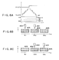
- Fig. 8B is a view schematically showing the positional relationship between each area of the information blocks and each of the probe electrodes at a certain time.
- the probe electrode 402 faces the block area 403 on the recording medium while the probe electrode 401 faces another block area 404 adjacent thereto on the recording medium. Then, by applying bias voltages V B1 , and V B2 each having the opposite polarities but same absolute values, the data in the block areas 403 and 404 are read with the probe electrodes which travel along the positions designated by the mark 0 sequentially as indicated by the arrow on each of the block areas as in the case shown in Fig. 2B.
- Fig. 8C is a schematic view the same as Fig. 8B and shows the state where the probe electrodes 401 and 402 have been traveled on the surface of the recording medium by the distance Xo in the same direction by the x-y stage 24 driven by the rough traveling driver 18 subsequent to the completion of the reading at the state shown in Fig. 8B, and by this shifting, the probe electrode 402 is caused to face the block area 404 and the probe electrode 401, another block area 405 adjacent thereto on the recording medum. Then, Fig. 8C further illustrates the probe electrodes reading the data in the block areas 404 and 405 with the driving waveforms shown in Fig. 8A as in the case of Fig. 8B.
- the block area 404 is scanned in the same track by the bias voltages having opposite polarities to each other such as minus in the first stage and plus in the second stage but the same absolute values. As a result, the charge accumulated on the recording medium 21 is offset. Then, the data reading in each of the block areas is performed two times each by the probe electrodes 401 and 402. In the respect, the minus voltage is applied by the probe electrode 401 in the first stage to the block area 402, and the plus voltage by the probe electrode 402 in the second stage, for example.
- Fig. 8D is a view showing each of the voltages applied at the time of information recording with the use of the same timing chart shown in Fig. 8A.
- the value of voltage V B in the period represented by "off” should be the value suited for detecting the tunnel current J T to control the averaged space between each of the probe electrodes and the recording medium 21 constantly by the space controlling means to control the distance therebetween. This value should be smaller than the threshold value generating the change (shifting to the "on” state) in the medium 21.
- the state in which the value of the voltage V B is the same during the period represented by “off”, should be maintained in the most part of the period so that the value of the voltage V B should exceed the threshold value in the last short period.
- each of the probe electrodes 401 and 402 is driven relatively against the recording medium 21 as in the case of the information reproducing, and when both probe electrodes scan the same block area, the voltages having different waveforms are applied only at the point where the polarities are changed as V B1 and V B2 shown in Fig. 8D.
- the same effect as in the information reproducing can be obtained. Also, particularly, by writing information plural times (two times) on the same block area, it is possible to implement a recording and reproducing apparatus capable of avoiding writing failure.
- a pair of probe electrodes having opposite polarities but the equal absolute values are driven to travel X o by X o as mentioned above to scan the block areas to reproduce information one after another, thus making it possible to offset the accumulated changes in the entire areas of the recording medium.
- Fig. 9 is a view partially showing the structure of a sixth embodiment according to the present invention. With the exception of the aspects set forth below, the structure of the present embodiment is the same as the one shown in Fig. 1. Accordingly, Fig. 9 illustrates only a part of its structure.
- the sixth embodiment is characterized in that provided is a photo-conductive extrathin film layer 501 connected to the substrate electrode on the recording medium 21 having the electric memory effect and grounded, and that after the recording and reproducing is performed by the probe electrode 10 under the state that the photoconductivity layer 501 is made highly resistive, the photoconductive layer 501 is irradiated by light from a light source 502 to make it low resistive.
- a numeral 504 designates a cover shielding the system from the outside; and 503, the grounding point of the photoconductive extrathin film layer 501 and the substrate electrode 22.
- the charge is accumulated in the recording medium or on the surface thereof by the probe electrode 10 to perform recording and reproducing, it is possible to discharge the accumulated charge in the recording medium or on the surface thereof by making the photoconductivity layer 501 low resistive with the light irradiation from the light source 502 after recording and reproducing as well as by the grounding point to which the layer 501 is connected together with the substrate electrode 22, thereby offsetting the remaining charge.
- the recording and reproducing can be performed by well known methods such as disclosed in Japanese Patent Laid-Open Application No. 63-161552, Japanese Patent Laid-Open Application No. 63-161553, and others.
- Fig. 10 is a view showing a seventh embodiment of the recording and reproducing apparatus according to the present invention.
- Fig. 10 illustrates only a part of its structure.
- the seventh embodiment is characterized by having a grounding means connected to the substrate electrode 22 for the grounding and capable of arbitrarily selecting the electrical non-connecting state or connecting state against the recording medium.
- a movable grounding plate 601 capable of traveling along the surface of the recording medium and of contacting closely with an arbitrary surface thereof, is used as the grounding means.
- the movable grounding plate 601 is connected to the substrate electrode 22 and is grounded as designated by a numeral 602.
- the seventh embodiment is such that after the recording and reproducing by the probe electrode 10 using the well known method as in the sixth embodiment, the movable grounding plate 601 is allowed to be in contact with the surface of the recording medium closely to discharge the accumulated charge on the surface of the redording medium or in its inside.
- Fig. 11 is a view showing an eighth embodiment of the present invention.
- Fig. 11 illustrates only a part of its structure.
- the eighth embodiment is characterized in that the charge deposited in the recording medium or on the surface thereof is neutralized by spreading charged particles over the surface of the recording medium.
- numeral 701 designates a corona discharging unit.
- the corona discharge with an appropriate amount of the charged particles having polarity offsetting the accumulated charge of the applied voltage V B is performed by the use of the corona discharging unit 701.
- the present invention is not limited thereto, and it may be possible to use a medium which enables a gold thin film to generate changes in shape as the medium having the electric memory effect, for example.
- the present invention is applicable to the case that the recording is made onto such medium and the information reproducing is performed by detecting the shapes recorded. In some cases, even if a gold thin film is used, the charge may also be accumulated on the extreme vicinity of the surface, and if there is such problem, the present invention can be expected to obtain the aforesaid advantages.
- the above-mentioned first through sixth embodiments are particularly characterized in that the driving voltage Vy in the axial direction Y has the staged waveforms, and the driving voltage V x in the axial direction X has the staged waveforms of different frequency in synchronism with Vy, and the average of applied voltages is zero in the period during which the application state of (V x , Vy) is selected in condition that the waveforms of the voltages applied to the recording medium are in synchronism with V x and Vy, i.e., the suspension period at the positions designated by the mark 0.
- the present invention is not limited thereto.
- the present invention may also be applicable to an apparatus which performs only recording or reproducing.
- the present invention can suitably be used for the STM system and its application equipment employed as an information reading apparatus.
Abstract
Description
- The present invention relates to an apparatus for reading and/or inputting information and a method therefor. More particularly, the present invention relates to an apparatus for reading and/or inputting information and a method therefor by applying a voltage to a recording medium when information is read or inputted.
- The present information is particularly suited for a recording and reproducing apparatus utilizing the principle of the scanning tunnel microscope (STM).
- In recent years, the use of memory materials has been the core of electronics industries such as computers and its peripheral equipment, video discs, and digital audio discs, and the development of the materials is in progress quite actively. Although the required capability of the memory material depends on its usage, such material should have the advantages given below in general among others.
- ① High-density and large recording capacity
- ②Quick responsibility to recording and reproducing
- ③ Small power consumption
- ④ High-productivity and low cost
- Traditionally, semiconductor memories and magnetic memories using magnetic substance or semiconductor as its material have been employed in most cases. In recent years, however, along with the evolution of the laser technology, inexpensive and high-density recording media by optical memories using organic thin film such as organic coloring matter and photopolymer have come to the fore.
- Meanwhile, a scanning tunnel microscope (hereinafter referred to as "STM") capable of directly observing the structure of electron on the surface atom of a conductor has recently been developed [G. Binnig et al., Helvetica Physica Acta, 55, 726 (1982)], and it becomes possible to measure a real space image with high resolution irrespective of a single crystalline or amorphous medium, yet without causing any damage thereto by its advantage that the observation is possible with a low electric power. Further, since the STM is operative in the atmosphere as well as usable for various kinds of materials, a wide range of the applications is anticipated.
- The STM utilizes the fact that when a metallic probe (probe electrode) and a conductive substance approach to each together up to a distance of approximately 1 nm while a voltage is being applied therebetween, a tunnel current flows. This current is quite sensitive to the difference in the distances between them. Therefore, it is possible to draw the surface structure in a real space by enabling the probe to scan so that a constant tunnel current is maintained, and at the same time to read various information concerning the entire electron cloud. At this juncture, the resolution in the direction toward the inner surface is approximately 1 Å. Accordingly, by applying the principle of the STM it is possible to perform a high-resolution recording and reproducing with an atomic order (several Å) satisfactorily. At a recording and reproducing methods in this case, there has been proposed a method for recording performed by changing the surface condition of an appropriate recording layer using a high-energy magnetic wave of corpuscular rays (electron beam or ion beam) or X-rays and an energy beam of visible or ultraviolet rays and then reproducing by the STM. Alternatively, there is a method for recording and reproducing using the STM by the use of a material as a recording layer, which has memory effects with respect to the voltampere switching characteristics, such as a thin film layer of an organic compound of 7T electron system, chalcogen compound or the like.
- However, it is required to apply a voltage in a constant direction from the probe to the medium intermittently or continuously at the time of recording or reproducing in the conventional method using the STM principle. For example, therefore, in the case where the medium has an organic thin film which is not conductive, or the like, the charge is accumulated on the surface of the medium thereby. There is a possibility that due to the accumulated charge floating molecules are absorbed onto the surface of the medium, or the organic thin film or the like is caused to be degraded or decomposed.
- Particularly, in the case of the recording and reproducing method using the STM principle, the recording and reproducing are performed in an area of an extremely narrow molecular order as compared with the conventional systems. Therefore, even an extremely small absorption of molecule to the surface of the recording medium, which should be negligible in the usual floppy disc type magnetic or optomagnetic recording and reproducing apparatus, or an extremely slight degradation or decomposition of the film quality, may cause a failure in writing or an error in reading.
- We have found there is a possibility that the charge generated as described above adversely affects on the recording and reproducing whereas the charge is not essentially related to these recording and reproducing, when the information is recorded onto the medium having an effect of changing the characteristic or the shape of the medium by applying voltage upon inputting of information or an effect capable of detecting said changes by applying voltage upon reading of information (in the present specification, such effects are referred to as "electric memory effect"), by applying voltage to thereby cause the electric memory effect, or when the information recorded by the electric memory effect is reproduced by applying voltage.
- In consideration of the aforesaid conventional example, a first object of the present invention is to provide an apparatus for reading and inputting of information with medium having said electric memory effect by applying voltage in which the absorption of molecule, the degradation and decomposition of the medium and the like are eliminated, thus preventing the errors in reading and in putting information.
- The other objects of the present invention will be clear from the detailed description of the embodiments thereof to be given later.
-
- Fig. 1 is a view schematically showing the structure of a first embodiment of an information recording and reproducing apparatus according to the present invention;
- Fig. 2A and Fig. 2B are a time chart showing driving voltage and applied voltage at the time of information recording in the apparatus, and a view schematically showing manner of information recording in the state of voltages, respectively;
- Fig. 3 is a time chart showing driving voltage and applied voltage at the time of information reproducing in the apparatus;
- Fig. 4 is a time chart showing driving voltage and applied voltage at the time of information recording in an information recording and reproducing apparatus of a second embodiment according to the present invention;
- Fig. 5 is a time chart showing driving voltage and applied voltage at the time of information recording in an information recording and reproducing apparatus a third embodiment according to the present invention;
- Fig. 6A and Fig. 6B are a time chart showing driving voltage and applied voltage at the time of information reproducing in an information recording and reproducing apparatus of a fourth embodiment according to the present invention, and a time chart showing driving voltage and applied voltage at the time of information recording in the apparatus, respectively;
- Fig. 6C is a view schematically showing manner of information recording and reproducing in the apparatus;
- Fig. 7 is a view schematically showing an information recording and reproducing apparatus of a fifth embodiment according to the present invention;
- Fig. 8A is a time chart showing driving voltage and applied voltage at the time of information reproducing in the apparatus;
- Fig. 8B and Fig. 8C are views schematically showing positional relationship between each of the probes and each of the block areas in the apparatus;
- Fig. 8D is a time chart showing driving voltage and applied voltage at the time of information recording in the apparatus;
- Fig. 9 is a schematic view partially showing structure of an information recording and reproducing apparatus of a sixth embodiment according to the present invention;
- Fig. 10 is a schematic view partially showing structure of an information recording and reproducing apparatus of a seventh embodiment according to the present invention; and
- Fig. 11 is a schematic view partially showing structure of an information recording and reproducing apparatus of an eighth embodiment according to the present invention.
- Fig. 1 is a view showing the structure of the recording and reproducing apparatus of a first embodiment according to the present invention. In Fig. 1, a numeral 10 designates a probe electrode; 22, a substrate electrode; and 21, a recording medium having the electric memory effect, which is sandwiched between the
probe electrode 10 andsubstrate electrode 22. Thesubstrate electrode 22 andrecording medium 21 are formed integrally on asubstrate 23. A numeral 15 designates a voltage application means to apply a voltage between theprobe 10 andsubstrate electrode 22, and generate a voltage VB. A numeral 17 designates a current detection means to detect a current flowing between theprobe electrode 10 andrecording medium 21; 12, a Z-direction fine traveling control mechanism to cause theprobe electrode 10 to be traveled in the Z direction finely; 16, a servo circuit to control the distance (Z direction) between theprobe electrode 10 andrecording medium 21 using the Z-direction fine travelingcontrol mechanism 12 on the basis of the current detection means 17. Theservo circuit 16, current detection means 17, and Z-directionfine traveling mechanism 12 constitute a part of a space controlling means to control the distance between theprobe 10 andrecording medium 21. In the current detection means 17, a numeral 201 designates a primary current-voltage converter having a sufficiently small inner resistance y as compared with the resistance between theprobe electrode 10 andsubstrate electrode 22, which outputs the detected current value after having converted it into a sufficiently large voltage signal corresponding thereto. Also, anumeral 202 designates a converter for converting the voltage signal containing the signed (positive or negative) current (JT) received from the current-voltage converter 201 to a signal corresponding to a logarithmic value log I JT of the absolute value of the JT, and the output therefrom is transmitted to adifferential divider 203. Thedifferential divider 203 outputs the difference between asignal 206 and a signal corresponding to the log | JT |, thesignal 206 corresponding to the logarithmic value of the predetermined value of the tunnel current defined so as to make the space between theprobe electrode 10 and recording medium 21 a predetermined value. This differential signal is transmitted to afrequency filter 204 thereby to cut the high-frequency signal corresponding to the recording information. A numeral 205 designates an amplifier circuit for amplifying a signal which has passed through thefilter 204. The signal passed through theamplifier circuit 205 becomes an information signal having an averaged space (averaged space of an area sufficiently larger than the recording bit) between therecording medium 21 andprobe 10, which is transmitted to amicrocomputer 19. Then, on the basis of this information signal, themicrocomputer 19 transmits an instruction signal to theservo circuit 16 so as to make the averaged space between theprobe electrode 10 andrecording medium 21 constant. - Also, a part of the output of the
converter 202 is directly transmitted to themicrocomputer 19 through afrequency filter 207 which passes a high-frequency signal and cuts a low frequency signal such as corresponding to the averaged space information between theprobe electrode 10 andrecording medium 21. At the time of information reproducing, this signal becomes the recording information signal, which is processed by themicrocomputer 19 to reproduce. - A numeral 11 designates an x-y direction fine traveling control mechanism for driving finely the
probe electrode 10 and fine travelingcontrol mechanism 12 in the x-y direction to cause theprobe electrode 10 to travel finely along the surface of therecording medium 21.Numerals control mechanism 11, respectively. The x-y direction fine travelingcontrol mechanism 11 causes theprobe electrode 10 to be displaced in the x-y directions in accordance with the voltage value applied respectively by thedrivers substrate 23 to travel in the X-Y directions roughly; 25, a rough traveling mechanism to cause thex-y stage 24 to travel in the Z direction roughly; 18, a rough traveling driver to transmit controlling signals to thex-y stage 24 andrough traveling mechanism 25 in accordance with the instruction signals from themicrocomputer 19; and 26, a support base. - Now, the operation of the recording and reproducing in the structure set forth above will be described.
- Fig. 2A and Fig. 2B illustrate the changes per time t in the x and y direction driving control voltages Vx and Vy and the applied voltage VB by the voltage application means 15 at the time of information recording, i.e., the output states of the
drivers microcomputer 19 and themeans 15 as well as the manner in which the recording is performed at that time. The upper stage of Fig. 2A shows the waveforms per time of the Y-axial driving control voltage Vy applied to the x-y direction fine travelingcontrol mechanism 11 which causes theprobe electrode 10 to travel along the surface of therecording medium 21; the middle stage thereof, the waveforms per time of the driving control voltage Vx in the X axial direction applied to the x-y fine travelingcontrol mechanism 11; and the lower stage thereof, the waveforms per time of the voltage applied between theprobe 10 andsubstrate electrode 22. Fig. 2A is a time chart of the applied voltage at the time of recording, and Fig. 2B is a view schematically showing the manner in which information is written onto the recording medium according to the time chart shown in Fig. 2A as an example. - When the voltage Vx and voltage Vy are applied as shown in the upper and middle stages of Fig. 2A, the tip of the
probe electrode 10 travels along arrows sequentially over the positions represented by 0 on therecording medium 21 as shown in Fig. 2B. The traveling of theprobe electrode 10 is substantially instantaneous, and theprobe electrode 10 stops at the positions represented by 0 for a predetermined period of time. In the lower stage of Fig. 2A, this predetermined period of time is shown bynumerals 31 to 40 per each position represented by mark 0 , and also in each of the positions marked 0 , the position at which a predetermined voltage is applied to generate a change in therecording medium 21, is represented by slanted lines in 0 in Fig. 2B. (This change, for example, is a shift from the off-state to on-state in a recording medium showing the memory switching characteristics as disclosed in Japanese Patent Laid-Open Application No. 63-161552). Further, the period during which the voltage causing such change is applied is represented by "on" in Fig. 2A, and all the other periods, by "off". Hereinafter, in the other embodiments which will be described later, the representation is also made by "on" and "off" in the same manner as in this case. - In the lower stage of Fig. 2A, the
broken line 41 shows the upper potential level (zero level) of therecording medium 21, and thebroken line 42 shows the threshold potential which causes therecording medium 21 at the phase level indicated by thebroken line 41 to change (shifting to the on-state), respectively. In the present embodiment, each of the recording bit positions, i.e. in each of the periods 31 - 40, the value of time integration [f VB (t) dt], of the applied voltage VB (voltage between the medium 21 and probe electrode 10) to the recording medium is substantially zero. In other words, the averaged value of VB in each of the periods becomes substantially zero. Specifically, when there is no application of the voltage changing the state of medium, which is represented by "off", the absolute value of the applied voltage VB should be equalized at half point in each of the periods to inverse plus and minus. The absolute value of the applied voltage VB at this time should be the value suited for detecting the tunnel current JT in order to control the average space between theprobe electrode 10 andrecording medium 21 constantly by the space controlling means for controlling the distance between theaforesaid probe electrode 21. This value should be defined to be smaller than the threshold value to generate a change in the medium 21 (to change the state to be "on"), and if the absolute value is equal, there is no substantial change in the output from theconverter 202 even when the sign of the applied voltage VB changes. Thus, the aforesaid average space control is performed during this period without any substantial effect from such change in the sign of the voltage VB. Also, when the voltage changing the medium represented by "on" is applied, during the period represented by "on" the state in which the absolute value of the voltage VB is equal, should be maintained in the most part of the period and the sign of the voltage VB is inverted in the last short period and the value of the voltage VB is made to exceed thethreshold value 42. At this juncture, the value of the voltage should be adjusted to be [f VB (t) dt] = O.If a large value such as exceeding the threshold value is applied, the value of the tunnel current JT is increased during such period. However, since this change is short enough, the aforesaid space controlling means does not substantially cause theprobe electrode 10 to change its position in the Z direction practically by this change in the value of the tunnel current JT. In other words, at the time of the medium changing voltage being applied, the aforesaid averaged space control is executed continuously without receiving an effect produced by the application of a large voltage. - As the above describes, irrespective of whether the medium changing (shifting to the "on" state) is generated or not, the charge once accumulated by the voltage applied in one direction in a fine region at which each of the recording positions is a center is diffused by the voltage applied in the opposite direction with making the value of time integration of the applied voltage VB substantially zero in each of the entire recording bit positions (positions represented by 0 ), and this charged state is eventually returned to the potential state before the recording (removed electrically). Therefore, the potential state over the entire recorded area of the recording medium is not changed substantially. In this respect, it may be possible to define the voltage exceeding the threshold value, (i.e., the time at which the voltage exceeding the threshold value is applied during the period), at the start of each of the periods not at the end thereof.
- Particularly, as shown in the lower stage of Fig. 2A, in the first embodiment the sections selected by the
means 11 to enable theprobe electrode 10 to travel along the surface of therecording medium 21, have a point symmetry. In other words, during the period represented by "off" the waveforms of the applied voltage between theprobe electrode 10 andsubstrate electrode 22 in the fine region having each of the recording bit positions as its center have the point symmetry. By using the waveforms having the point symmetry as the waveform of the applied voltage corresponding to the periods represented by "off", not only it is possible to perform [ f VB (t) dt] = 0 easily in this period, but by making the pulses point symmetry, it is also possible to avoid and extremely intensified voltage to be applied locally in the region where no change is generated in the recording medium. - Also, particularly, as shown in the lower stage of Fig. 2A, in the first embodiment the sections selected by the
means 11 to enable theprobe electrode 10 to travel along the surface of therecording medium 21 in the waveforms in the periods represented by "on", have a point asymmetry. In other words, the waveforms of the voltage applied between theprobe electrode 10 andsubstrate electrode 22 in the fine region having each of the recording bit positions as its center have the point asymmetry to any points in the section. - By using the waveforms having the point asymmetric property to any other points as the waveforms of the applied voltage corresponding to the periods represented by "on", it becomes easy to apply an extremely intensified voltage locally under condition of [f VB (t) dt] = 0 within this period; making it possible to cause the medium change (shifting to the "on" state) more reliably than conventional case.
- As the
recording medium 21, an organic thin film having memory switching characteristics such as disclosed in Japanese Patent Laid-Open Application No. 63-161552 is considered applicable. - Here, an example is considered for a recording medium which shows the "on" state against an applied voltage having the threshold value of approximately three volts or more, while holding the "off" state against an applied voltage of approximately three volts or less without any change in its "on" state.
- In the waveforms of the applied voltage corresponding to the "on" state represented in the
periods recording medium 21, corresponding to the "on" state can be realized in condition that the value of time integration of the applied voltage in the fine region having each of the recording bits as its center is zero. - Also, in the waveforms of the applied voltage corresponding to the "off" state represented in the
periods recording medium 21, corresponding to the "off" state (here, the application of voltage by which the state of the medium is not particularly allowed to be changed) can be realized in condition that the value of time integration of the applied voltage in the fine region having each of the recording bits as its center is zero. - Subsequently, the information reproducing will be described.
- Fig. 3 is a view illustrating the changes per time t of the driving control voltages Vx and Vy in the x and y directions at the time of information reproducing, and of the applied voltage VB by the voltage application means 15. Fig. 3 is represented by the same time chart as shown in Fig. 2A. Here, the x-y direction driving of the x-y direction
fine traveling mechanism 11 portion including theprobe electrode 10 is the same as that of information recording, so its description is omitted. - As in the case of the information recording, the suspension periods of the
probe electrode 10 are designated bynumerals 131 to 140. At each of the recording bit positions also in information reproducing, i.e., in each of theperiods 131 to 140, the value of time integration [f VB (t) dt] of the applied voltage VB to the recording medium is substantially zero. Specifically, at half point of each period, the absolute value of the applied voltage VB should be equalized to invert plus and minus. The absolute value of the applied voltage VB at this time should be the value suited for detecting the tunnel current JT in order to control the averaged space between theprobe electrode 10 andrecording medium 21 constantly by the space controlling means therebetween and to reproduce information. It is needless to mention that this value is smaller than the threshold value which generates changes in the medium 21. If the absolute value is equal, the output from theconverter 202 does not practically changes even when the sign of the applied voltage VB changes, and during this period, the averaged space control and the reproducing of the recorded information are executed without receiving any substantial effect from changes in the sign of the applied voltage VB. - Now, since the information reproducing operation is repeatedly performed, the charge is accumulated by the applied voltage, and it is more liable to generate the molecular absorption on the surface of the recording medium or the degradation or deterioration of the film quality than that of the information recording. Therefore, it is particularly effective to make [ ∫ VB (t) dt] = 0 at each of the recording bit positions.
- Also, in consideration of the repeating operation of the information reproducing, it is particularly effective to avoid by the waveforms having the point symmetry any extremely intensified voltage which is locally applied.
- Fig. 4 is a time chart showing the application state of each of the voltages Vx, Vy, and VB per time t when the information recording is performed by a recording and reproducing apparatus of a second embodiment according to the present invention. The structure of the apparatus is the same as shown in Fig. 1, and the application state of each of the voltages Vx, Vy, and VB per time t when the information reproducing is performed, is the same as shown in Fig. 3. Further, the x-y direction driving of the
probe electrode 10 is the same as described in conjunction with Fig. 2. Therefore, its description of these aspects are omitted. - The second embodiment is characterized in that before or after or both before and after (in Fig. 4, the case of only before is shown) the application of a large voltage exceeding the aforesaid threshold value during the "on" period represented in the lower stage of Fig. 4, the pulse having the voltage with an inverted sign, which is slightly larger than the voltage for detecting the tunnel current JT, (but does not exceed the threshold value) is once added. (Hereinafter, this pulse voltage is referred to as "auxiliary pulse").
- That is, the present embodiment is characterized by having the auxiliary pulses (designated by
numerals 61 to 66) whose absolute voltages are intensified in the opposite polarity to written pulse before thepulse portions 51 to 56 with the voltage exceeding the threshold value (i.e. the written pulse), in the waveforms during the period represented by "on" in Fig. 4. Hence, it is possible to make the absolute value of the written pulse voltage large with ease under the condition of [f VB (t) dt] = 0 in this period, and to execute the medium change (shifting to the "on" state) more reliably. The period of the auxiliary pulse should be short enough so that the change in the tunnel current JT upon the auxiliary pulse application does not have an effect on the control for making the averaged space between theprobe electrode 10 andrecording medium 21 constant by said space controlling means. However, in the case where theprobe electrode 10 tends to travel following the changes in the tunnel current JT upon the application of the written pulse or the auxiliary pulse (i.e. gain being great) due to a slightly intensified feedback of the space controlling means, the space between theprobe electrode 10 andrecording medium 21 can be made larger once prior to the application of the written pulse, by adding thisauxiliary pulses 61 to 66. If the space is made large in advance as this case, the changes in the tunnel current JT upon the written pulse application can be made small, and an effect is obtainable to prevent the space controlling means from becoming unstable. - This second embodiment is also characterized by having the pulse voltages (auxiliary pulses) with a comparatively large point symmetry designated by
numerals 71 to 74 and 81 to 84 provided before and after the boundary where the signs of the voltage VB are changed, in the waveforms of the applied voltage corresponding to the period represented by "off". In the case where the space controlling means possesses a slightly intensified feedback, it is possible by this feature as in the period represented by "on" to change the voltage polarities while keeping theprobe electrode 10 slightly away from the surface of the recording medium. There are some cases where depending on the material of the recording medium, an adverse effect such as the deterioration of quality thereof is observed due to the rapid inverting of the polarity. However, by inverting the polarity after the space has once been made larger, the electric field in therecording medium 21 is changed, whereby an effect is obtainable to change the electric field in therecording medium 21 comparatively smoothly together with the nonlinearity of the tunnel current. - Fig. 5 is a view showing a third embodiment according to the present invention.
- The third embodiment is the same as the first embodiment with the exception of the aspects set forth below. Therefore, the description is made only by the same time chart as shown in Fig. 2A. The third embodiment is characterized in that in the waveforms of the applied voltage in the period represented by "off", when the absolute value of the applied voltage VB is equalized to invert plus and minus as in the case of the first embodiment, there are provided a plurality of periods with at least three or more periods where the voltage VB is constant before and after this inverting portion, and portions in which the level of the relative voltage is gradually decreased or increased in the plurality of periods.
- As the above describes, by changing the level of the relative voltage gradually, it is possible to change the signs of the voltage VB smoothly under condition of [f VB (t) dt] = 0 in this period, and to prevent the space controlling means from becoming unstable due to a rather large current to be generated by the accumulated charge when the polarity of the applied voltage is changed rapidly as well as the quality of the recording medium from being deteriorated due to the rapid change of the polarity.
- In other words, the third embodiment has the auxiliary pulse in the direction in which | VB is made small, before and after the boundary where the signs of the voltage VB are changed in the waveforms in the periods represented by "off". This auxiliary pulse is effective when the feedback of the space controlling means is weak (gain being small).
- The third embodiment is also characterized by having the auxiliary pulses (designated by
numerals 101 to 106) whose absolute voltages are intensified in the direction of the opposite polarity to the written pulses after the writtenpulse portions 91 to 96, in the waveforms of the applied voltage in the period represented by "on". Thus, as in the case of the auxiliary pulses of the second embodiment, it becomes easy to make the absolute value of the pulse voltage large under the condition of [f VB (t) dt] = 0 during this period, and to perform the medium change (shifting to the "on" state) more reliably. - Figs. 6A and 6B are views showing a fourth embodiment according to the present invention. The fourth embodiment is also the same as the first embodiment with the exception of the aspects given below. Therefore, the description will be made only by the same time chart as in Fig. 3. The fourth embodiment is recording and reproducing systems characterized in that when the
probe electrode 10 is traveled along the surface of therecording medium 21 to scan a plurality of frames (one transversal row designated by the reference mark 0 in Fig. 2B is assumed to be one frame) at the time of information recording and reproducing, applied voltages between the probe electrode and the recording medium are defined so that the integration average of the voltages applied between the probe electrode and substrate electrode in scanning the plurality of frames should become substantially zero. - In particular, the fourth embodiment is characterized in that performed is the recording and reproducing of the information block which is the frame scanning in which the probe electrode is scanned along the surface of the recording medium in even-numbered times, i.e., 2N-times (where N is a natural arbitrary number), and the absolute value of the applied voltage between the
probe electrode 10 andrecording medium 21 is equalized at the time of one N-time frame scanning and the remaining N-time frame scanning in the frame scanning of the even-numbered times (2N) to change the voltage polarities (plus and minus) each other (this changing being performed in the odd-numbered time and even-numbered time, for example), whereby the value of time integration of the applied voltage VB is made substantially zero for the block as a whole. - Particularly, the present embodiment is characterized in that the recording and reproducing of the information block requiring a two-time frame scanning are performed, and that the absolute values of the applied voltages between the probe electrode and recording medium in the two-time frame scanning are equalized to change the voltage polarities each other so as to make the value of time integration of the applied voltage VB substantially zero in each of the two frames.
- Fig. 6A is a time chart at the time of information reproducing and Fig. 6B is a time chart at the time of information recording.
- In Figs. 6A and 6B, a numeral 301 designates the frame scanning period for a first time; 302, the frame scanning period for a second time. Also, in Figs. 6A and 6B, reference marks Vy and Vx designate the driving waveforms of the same means 11 to cause the probe electrode to travel along the surface of the recording medium as in Fig. 2A, and in the frame scanning portion for the first time and the frame scanning portion for the second time, the probe electrode is arranged to travel in the opposite directions while drawing the same track on the recording medium. The manner of recording and reproducing at this juncture, i.e., the way of traveling of the
probe electrode 10, are represented in Fig. 6C using the same schematic view of Fig. 2B. - In Fig. 6A, the voltage VB is VB = + VBO -(where VBO is a constant) for the frame scanning period for the first time, and VB = - VBO for the frame scanning period for the second time.
- In Fig. 6B, the voltage VB is defined to provide its value of VB equivalent to a value suited for detecting the tunnel current JT in the Period represented by "off" during the
frame scanning period 301 in order to control the averaged space between theprobe electrode 10 andrecording medium 21 constantly by the space controlling means for controlling the distance therebetween. This value should be smaller than the threshold value generating a change (shifting to the "on" state) in the medium 21. - Also, during the application period (represented by "on") of the voltage changing the medium, the state where the value of the voltage VB is equal to the one during the period represented by "off" is maintained in the most part of this period, and the value of the voltage VB should be made to exceed the threshold only in the last short period. Then, in the
frame scanning period 301 after the completion of the scanning for the first time, the voltage application at each position during theframe scanning period 301 is repeated at the same position in the same manner while inverting the polarities of the waveforms of the respective applied voltages. - In the fourth embodiment, the accumulation of the surface charge to the surface of the recording medium is prevented by defining the applied voltage between the probe electrode and recording medium to make the integration average at each position substantially zero in a plurality of frame scannings.
- Also, in particular, it is possible to inspect whether or not the data reading has been performed correctly by executing the reading with a plurality of frame scannings. For example, information for detecting errors is provided in one information block, and it may be possible to output the information which has been read with the least error as a correctly reproduced information among those plural readings at the time of reproducing.
- Likewise, by writing information onto the recording medium for plural times (two times), a recording and reproducing apparatus particularly capable of avoiding writing failure can be implemented.
- Now, in conjunction with Fig. 7 and Figs. 8A to 8D, a fifth embodiment according to the present invention will be described.
- Fig. 7 is a view schematically showing the structure of the fifth embodiment. The fifth embodiment is an apparatus for recording, reproducing, and erasing by the use of a plurality of probe electrodes having means to enable them to travel along the surface of the recording medium. In Fig. 7,
reference numerals probe electrode 10 shown in Fig. 1, respectively. The proveelectrode 401 is provided with a x-y direction fine travelingcontrol mechanism 11 a, z-direction fine travelingcontrol mechanism 12a, y-axial scanning driver 13a,x-axial scanning driver 14a, voltage application means 15a,servo circuit 16a, and current detection means 17a as in the case of Fig. 1. The operation of each constituent is substantially the same as each of those described in the first embodiment. - The
probe electrode 402 is also provided with a x-y direction fine travelingcontrol mechanism 11 b, z-direction fine travelingcontrol mechanism 12b, y-axial scanning driver 13b,x-axial scanning driver 14b, voltage application means 15b, servo circuit 16b, and current detection means 17b as in the case of Fig. 1. The operation of each constituent is substantially the same as each of those described in the first embodiment. Theprobe electrodes driver 18, anx-y stage 24 is driven to cause each of the probe electrodes to travel evenly Xo by Xo to perform recording and reproducing. The present embodiment is a recording and reproducing apparatus wherein the integration average of the voltages applied between the plural electrodes and the substrate electrode at each bit on the recording medium in a certain period is substantially zero. - In particular, the present embodiment is characterized in that the recorded data in a certain block in the recording medium is read by the use of a pair of
probe electrodes - In Fig. 7, the
probe electrodes - Fig. 8A is the same time chart as Fig. 2A which shows each of the voltages applied to the two
probe electrodes - Here, with the exception of the central positions which are different, the
probe electrodes - Fig. 8B is a view schematically showing the positional relationship between each area of the information blocks and each of the probe electrodes at a certain time.
- At the time represented by Fig. 8B, the
probe electrode 402 faces theblock area 403 on the recording medium while theprobe electrode 401 faces anotherblock area 404 adjacent thereto on the recording medium. Then, by applying bias voltages VB1, and VB2 each having the opposite polarities but same absolute values, the data in theblock areas - Fig. 8C is a schematic view the same as Fig. 8B and shows the state where the
probe electrodes x-y stage 24 driven by the rough travelingdriver 18 subsequent to the completion of the reading at the state shown in Fig. 8B, and by this shifting, theprobe electrode 402 is caused to face theblock area 404 and theprobe electrode 401, anotherblock area 405 adjacent thereto on the recording medum. Then, Fig. 8C further illustrates the probe electrodes reading the data in theblock areas - With the operation set forth above, the
block area 404 is scanned in the same track by the bias voltages having opposite polarities to each other such as minus in the first stage and plus in the second stage but the same absolute values. As a result, the charge accumulated on therecording medium 21 is offset. Then, the data reading in each of the block areas is performed two times each by theprobe electrodes probe electrode 401 in the first stage to theblock area 402, and the plus voltage by theprobe electrode 402 in the second stage, for example. - Fig. 8D is a view showing each of the voltages applied at the time of information recording with the use of the same timing chart shown in Fig. 8A. The value of voltage VB in the period represented by "off" should be the value suited for detecting the tunnel current JT to control the averaged space between each of the probe electrodes and the
recording medium 21 constantly by the space controlling means to control the distance therebetween. This value should be smaller than the threshold value generating the change (shifting to the "on" state) in the medium 21. - Also, during the period of applying the medium changeing voltage, which is represented by "on", the state in which the value of the voltage VB is the same during the period represented by "off", should be maintained in the most part of the period so that the value of the voltage VB should exceed the threshold value in the last short period.
- Then, each of the
probe electrodes recording medium 21 as in the case of the information reproducing, and when both probe electrodes scan the same block area, the voltages having different waveforms are applied only at the point where the polarities are changed as VB1 and VB2 shown in Fig. 8D. By repeating this process for each of the block areas, the same effect as in the information reproducing can be obtained. Also, particularly, by writing information plural times (two times) on the same block area, it is possible to implement a recording and reproducing apparatus capable of avoiding writing failure. - As the above describes, in the fifth embodiment, a pair of probe electrodes having opposite polarities but the equal absolute values are driven to travel Xo by Xo as mentioned above to scan the block areas to reproduce information one after another, thus making it possible to offset the accumulated changes in the entire areas of the recording medium.
- Also, by the use of a plurality of probe electrodes to remove the charges electrically, it is possible to write or read information onto or from the recording medium plural times (two times) without prolonging the reading or writing time, and to implement effectively a recording and reproducing apparatus capable of avoiding the possibility of writing failure or reading error.
- Fig. 9 is a view partially showing the structure of a sixth embodiment according to the present invention. With the exception of the aspects set forth below, the structure of the present embodiment is the same as the one shown in Fig. 1. Accordingly, Fig. 9 illustrates only a part of its structure.
- The sixth embodiment is characterized in that provided is a photo-conductive
extrathin film layer 501 connected to the substrate electrode on therecording medium 21 having the electric memory effect and grounded, and that after the recording and reproducing is performed by theprobe electrode 10 under the state that thephotoconductivity layer 501 is made highly resistive, thephotoconductive layer 501 is irradiated by light from alight source 502 to make it low resistive. - In Fig. 9, a numeral 504 designates a cover shielding the system from the outside; and 503, the grounding point of the photoconductive
extrathin film layer 501 and thesubstrate electrode 22. Although the charge is accumulated in the recording medium or on the surface thereof by theprobe electrode 10 to perform recording and reproducing, it is possible to discharge the accumulated charge in the recording medium or on the surface thereof by making thephotoconductivity layer 501 low resistive with the light irradiation from thelight source 502 after recording and reproducing as well as by the grounding point to which thelayer 501 is connected together with thesubstrate electrode 22, thereby offsetting the remaining charge. In the present embodiment, the recording and reproducing can be performed by well known methods such as disclosed in Japanese Patent Laid-Open Application No. 63-161552, Japanese Patent Laid-Open Application No. 63-161553, and others. - Fig. 10 is a view showing a seventh embodiment of the recording and reproducing apparatus according to the present invention.
- With the exception of the aspects set forth below, the structure of the seventh embodiment is also the same as the one shown in Fig. 1. Accordingly, Fig. 10 illustrates only a part of its structure. The seventh embodiment is characterized by having a grounding means connected to the
substrate electrode 22 for the grounding and capable of arbitrarily selecting the electrical non-connecting state or connecting state against the recording medium. - In particular, a
movable grounding plate 601, capable of traveling along the surface of the recording medium and of contacting closely with an arbitrary surface thereof, is used as the grounding means. Themovable grounding plate 601 is connected to thesubstrate electrode 22 and is grounded as designated by a numeral 602. - The seventh embodiment is such that after the recording and reproducing by the
probe electrode 10 using the well known method as in the sixth embodiment, themovable grounding plate 601 is allowed to be in contact with the surface of the recording medium closely to discharge the accumulated charge on the surface of the redording medium or in its inside. - Fig. 11 is a view showing an eighth embodiment of the present invention.
- With the exception of the aspects set forth below, the structure of the present embodiment is also the same as the one shown in Fig. 1. Accordingly, Fig. 11 illustrates only a part of its structure. The eighth embodiment is characterized in that the charge deposited in the recording medium or on the surface thereof is neutralized by spreading charged particles over the surface of the recording medium.
- In Fig. 11, numeral 701 designates a corona discharging unit. In other words, in the eighth embodiment, subsequent to the recording and reproducing by the
probe electrode 10 with the well known method as in the first embodiment, the corona discharge with an appropriate amount of the charged particles having polarity offsetting the accumulated charge of the applied voltage VB is performed by the use of thecorona discharging unit 701. - In the descriptions of the above-mentioned embodiments, while an organic film having memory switching characteristics is exemplified as the
recording medium 21, the present invention is not limited thereto, and it may be possible to use a medium which enables a gold thin film to generate changes in shape as the medium having the electric memory effect, for example. The present invention is applicable to the case that the recording is made onto such medium and the information reproducing is performed by detecting the shapes recorded. In some cases, even if a gold thin film is used, the charge may also be accumulated on the extreme vicinity of the surface, and if there is such problem, the present invention can be expected to obtain the aforesaid advantages. - The above-mentioned first through sixth embodiments are particularly characterized in that the driving voltage Vy in the axial direction Y has the staged waveforms, and the driving voltage Vx in the axial direction X has the staged waveforms of different frequency in synchronism with Vy, and the average of applied voltages is zero in the period during which the application state of (Vx, Vy) is selected in condition that the waveforms of the voltages applied to the recording medium are in synchronism with Vx and Vy, i.e., the suspension period at the positions designated by the mark 0. However, the present invention is not limited thereto.
- For example, it may be possible to make the driving voltage Vy in the axial direction Y, a voltage waveform of trigonometrical waveform, and the driving voltage Vx in the axial direction X, a voltage waveform of trigonometrical waveform of different frequency in synchronism with Vy. Even with this arrangement, it is possible to make the average of the applied voltages zero in the period during which the traveling probe electrode scans the area of one bit to plural bits portions in a state where the waveforms of voltages applied to the recording medium are in synchronism with Vx and Vy.
- Also, while the above-mentioned embodiments are recording and reproducing apparatus, the present invention may also be applicable to an apparatus which performs only recording or reproducing.
- Also, the present invention can suitably be used for the STM system and its application equipment employed as an information reading apparatus.
- With each of the embodiments set forth above, it becomes possible to perform a highly precise information reading or inputting at all times without producing any adverse effects on the information medium due to the charge accumulation caused by the applied voltage.
Claims (24)
Applications Claiming Priority (2)
| Application Number | Priority Date | Filing Date | Title |
|---|---|---|---|
| JP2205831A JP2744338B2 (en) | 1990-08-01 | 1990-08-01 | Apparatus and method for reading and / or inputting information |
| JP205831/90 | 1990-08-01 |
Publications (3)
| Publication Number | Publication Date |
|---|---|
| EP0469565A2 true EP0469565A2 (en) | 1992-02-05 |
| EP0469565A3 EP0469565A3 (en) | 1992-12-09 |
| EP0469565B1 EP0469565B1 (en) | 1996-12-18 |
Family
ID=16513435
Family Applications (1)
| Application Number | Title | Priority Date | Filing Date |
|---|---|---|---|
| EP91112832A Expired - Lifetime EP0469565B1 (en) | 1990-08-01 | 1991-07-30 | Apparatus for reading and/or inputting information |
Country Status (6)
| Country | Link |
|---|---|
| US (1) | US5204851A (en) |
| EP (1) | EP0469565B1 (en) |
| JP (1) | JP2744338B2 (en) |
| AT (1) | ATE146620T1 (en) |
| CA (1) | CA2048194C (en) |
| DE (1) | DE69123656T2 (en) |
Cited By (2)
| Publication number | Priority date | Publication date | Assignee | Title |
|---|---|---|---|---|
| EP0519745A2 (en) * | 1991-06-21 | 1992-12-23 | Canon Kabushiki Kaisha | Recording medium, information processing apparatus using same, and information-erasing method |
| EP0615235A2 (en) * | 1993-03-09 | 1994-09-14 | Canon Kabushiki Kaisha | Information recording method and information recording apparatus |
Families Citing this family (10)
| Publication number | Priority date | Publication date | Assignee | Title |
|---|---|---|---|---|
| JP2743213B2 (en) * | 1990-07-25 | 1998-04-22 | キヤノン株式会社 | Apparatus and method for recording and / or reproducing |
| JP3126409B2 (en) * | 1991-06-05 | 2001-01-22 | キヤノン株式会社 | Information recording and playback method |
| US5323377A (en) * | 1992-11-27 | 1994-06-21 | Chen Zhi Q | Electrical data recording and retrieval based on impedance variation |
| JPH06251435A (en) * | 1993-03-01 | 1994-09-09 | Canon Inc | Recording and reproducing device |
| JPH09320133A (en) * | 1995-10-16 | 1997-12-12 | Canon Inc | Device and method for recording and reproducing and bit detection method |
| JPH10213854A (en) * | 1997-01-30 | 1998-08-11 | Olympus Optical Co Ltd | Picture reader |
| US6195313B1 (en) * | 1997-08-29 | 2001-02-27 | Canon Kabushiki Kaisha | Tracking mechanism and method using probes for information recording/reproducing apparatus |
| JP2003045042A (en) * | 2001-07-31 | 2003-02-14 | Toshiba Corp | Thickness irregularity correction method for information recording medium and information recording and reproducing device using thickness irregularity correction method |
| KR100519752B1 (en) | 2002-05-10 | 2005-10-07 | 삼성전자주식회사 | High-speed high-density data storage apparatus employing time-division-multiplexing type and method of recording information using the same and method of reproducing information using the same |
| KR100519772B1 (en) * | 2002-10-14 | 2005-10-07 | 삼성전자주식회사 | Magnetic medium using spin-polarized electron and Apparatus of recording data and Recording method using the same |
Citations (7)
| Publication number | Priority date | Publication date | Assignee | Title |
|---|---|---|---|---|
| US2972082A (en) * | 1955-02-14 | 1961-02-14 | Research Corp | Data storage method and apparatus |
| GB896691A (en) * | 1958-06-09 | 1962-05-16 | Armour Res Found | Improvements in or relating to a transducer system and method |
| FR1318898A (en) * | 1962-02-28 | 1963-02-22 | Armour Res Found | Recording method and device |
| US3202973A (en) * | 1963-04-18 | 1965-08-24 | Ht Res Inst | Electrostatic reproducing apparatus |
| JPS57133534A (en) * | 1981-02-09 | 1982-08-18 | Toshiba Corp | Electrostatic recording system |
| EP0249199A1 (en) * | 1986-06-11 | 1987-12-16 | Manfred R. Kuehnle | Optoelectronic signal recording medium and method of making same |
| EP0327236A2 (en) * | 1988-01-24 | 1989-08-09 | Victor Company Of Japan, Limited | Image pickup apparatus |
Family Cites Families (4)
| Publication number | Priority date | Publication date | Assignee | Title |
|---|---|---|---|---|
| US4829507A (en) * | 1984-09-14 | 1989-05-09 | Xerox Corporation | Method of and system for atomic scale readout of recorded information |
| JP2556491B2 (en) * | 1986-12-24 | 1996-11-20 | キヤノン株式会社 | Recording device and recording method |
| JP2556492B2 (en) * | 1986-12-24 | 1996-11-20 | キヤノン株式会社 | Reproduction device and reproduction method |
| EP0307210A3 (en) * | 1987-09-10 | 1991-05-15 | Seiko Instruments Inc. | Memory writing apparatus |
-
1990
- 1990-08-01 JP JP2205831A patent/JP2744338B2/en not_active Expired - Fee Related
-
1991
- 1991-07-30 EP EP91112832A patent/EP0469565B1/en not_active Expired - Lifetime
- 1991-07-30 DE DE69123656T patent/DE69123656T2/en not_active Expired - Fee Related
- 1991-07-30 AT AT91112832T patent/ATE146620T1/en not_active IP Right Cessation
- 1991-07-30 US US07/738,113 patent/US5204851A/en not_active Expired - Lifetime
- 1991-07-31 CA CA002048194A patent/CA2048194C/en not_active Expired - Fee Related
Patent Citations (7)
| Publication number | Priority date | Publication date | Assignee | Title |
|---|---|---|---|---|
| US2972082A (en) * | 1955-02-14 | 1961-02-14 | Research Corp | Data storage method and apparatus |
| GB896691A (en) * | 1958-06-09 | 1962-05-16 | Armour Res Found | Improvements in or relating to a transducer system and method |
| FR1318898A (en) * | 1962-02-28 | 1963-02-22 | Armour Res Found | Recording method and device |
| US3202973A (en) * | 1963-04-18 | 1965-08-24 | Ht Res Inst | Electrostatic reproducing apparatus |
| JPS57133534A (en) * | 1981-02-09 | 1982-08-18 | Toshiba Corp | Electrostatic recording system |
| EP0249199A1 (en) * | 1986-06-11 | 1987-12-16 | Manfred R. Kuehnle | Optoelectronic signal recording medium and method of making same |
| EP0327236A2 (en) * | 1988-01-24 | 1989-08-09 | Victor Company Of Japan, Limited | Image pickup apparatus |
Non-Patent Citations (1)
| Title |
|---|
| PATENT ABSTRACTS OF JAPAN vol. 6, no. 233 (P-156)(1111) 19 November 1982 & JP-A-57 133 534 ( TOSHIBA DENKI K.K. ) 18 August 1982 * |
Cited By (5)
| Publication number | Priority date | Publication date | Assignee | Title |
|---|---|---|---|---|
| EP0519745A2 (en) * | 1991-06-21 | 1992-12-23 | Canon Kabushiki Kaisha | Recording medium, information processing apparatus using same, and information-erasing method |
| EP0519745B1 (en) * | 1991-06-21 | 1998-05-20 | Canon Kabushiki Kaisha | Recording medium, information processing apparatus using same, and information-erasing method |
| EP0615235A2 (en) * | 1993-03-09 | 1994-09-14 | Canon Kabushiki Kaisha | Information recording method and information recording apparatus |
| EP0615235A3 (en) * | 1993-03-09 | 1997-11-12 | Canon Kabushiki Kaisha | Information recording method and information recording apparatus |
| US5732053A (en) * | 1993-03-09 | 1998-03-24 | Canon Kabushiki Kaisha | Information recording method information recording apparatus |
Also Published As
| Publication number | Publication date |
|---|---|
| CA2048194A1 (en) | 1992-02-02 |
| JPH0490150A (en) | 1992-03-24 |
| DE69123656D1 (en) | 1997-01-30 |
| CA2048194C (en) | 1997-08-26 |
| EP0469565A3 (en) | 1992-12-09 |
| DE69123656T2 (en) | 1997-06-19 |
| US5204851A (en) | 1993-04-20 |
| ATE146620T1 (en) | 1997-01-15 |
| EP0469565B1 (en) | 1996-12-18 |
| JP2744338B2 (en) | 1998-04-28 |
Similar Documents
| Publication | Publication Date | Title |
|---|---|---|
| US4829507A (en) | Method of and system for atomic scale readout of recorded information | |
| EP0513790B1 (en) | Information processing apparatus | |
| US6195313B1 (en) | Tracking mechanism and method using probes for information recording/reproducing apparatus | |
| US4907195A (en) | Method of and system for atomic scale recording of information | |
| US5144581A (en) | Apparatus including atomic probes utilizing tunnel current to read, write and erase data | |
| EP0519745B1 (en) | Recording medium, information processing apparatus using same, and information-erasing method | |
| EP0174860A2 (en) | Information recording and readout | |
| US5204851A (en) | Apparatus for reading and/or inputting information | |
| US4826732A (en) | Recording medium | |
| US4878213A (en) | System for recording and readout of information at atomic scale densities and method therefor | |
| US5251200A (en) | Tracking method for memory apparatus | |
| US5202879A (en) | Information recording medium, and information recording and/or reproducing method and apparatus | |
| US5432771A (en) | Information recording/reproducing apparatus for performing recording/reproduction of information by using probe | |
| US5287342A (en) | Apparatus and method for reproducing information | |
| EP0518240B1 (en) | Information reproducing method and information reproducing apparatus which uses the method | |
| US5757760A (en) | Information recording and/or reproducing apparatus and method for performing recording and/or reproduction of information by using probe | |
| EP0640963B1 (en) | Recording and reproducing method and apparatus using a scanning probe | |
| JP2930449B2 (en) | Tracking method | |
| US5517482A (en) | Information recording/reproducing apparatus having fuzzy operating unit | |
| JP3015978B2 (en) | Information processing device | |
| JP2962603B2 (en) | Information recording method | |
| JP3004823B2 (en) | Information processing device | |
| RU2042982C1 (en) | Method for writing and reading binary information | |
| JP4079397B2 (en) | Tracking mechanism and tracking method for recording / reproducing apparatus | |
| JPH1173746A (en) | Tracking mechanism and tracking method |
Legal Events
| Date | Code | Title | Description |
|---|---|---|---|
| PUAI | Public reference made under article 153(3) epc to a published international application that has entered the european phase |
Free format text: ORIGINAL CODE: 0009012 |
|
| AK | Designated contracting states |
Kind code of ref document: A2 Designated state(s): AT BE CH DE DK ES FR GB GR IT LI LU NL SE |
|
| PUAL | Search report despatched |
Free format text: ORIGINAL CODE: 0009013 |
|
| AK | Designated contracting states |
Kind code of ref document: A3 Designated state(s): AT BE CH DE DK ES FR GB GR IT LI LU NL SE |
|
| 17P | Request for examination filed |
Effective date: 19930427 |
|
| 17Q | First examination report despatched |
Effective date: 19941115 |
|
| GRAG | Despatch of communication of intention to grant |
Free format text: ORIGINAL CODE: EPIDOS AGRA |
|
| GRAH | Despatch of communication of intention to grant a patent |
Free format text: ORIGINAL CODE: EPIDOS IGRA |
|
| GRAH | Despatch of communication of intention to grant a patent |
Free format text: ORIGINAL CODE: EPIDOS IGRA |
|
| GRAA | (expected) grant |
Free format text: ORIGINAL CODE: 0009210 |
|
| AK | Designated contracting states |
Kind code of ref document: B1 Designated state(s): AT BE CH DE DK ES FR GB GR IT LI LU NL SE |
|
| PG25 | Lapsed in a contracting state [announced via postgrant information from national office to epo] |
Ref country code: NL Free format text: LAPSE BECAUSE OF FAILURE TO SUBMIT A TRANSLATION OF THE DESCRIPTION OR TO PAY THE FEE WITHIN THE PRESCRIBED TIME-LIMIT Effective date: 19961218 Ref country code: LI Effective date: 19961218 Ref country code: GR Free format text: LAPSE BECAUSE OF FAILURE TO SUBMIT A TRANSLATION OF THE DESCRIPTION OR TO PAY THE FEE WITHIN THE PRESCRIBED TIME-LIMIT Effective date: 19961218 Ref country code: ES Free format text: THE PATENT HAS BEEN ANNULLED BY A DECISION OF A NATIONAL AUTHORITY Effective date: 19961218 Ref country code: DK Effective date: 19961218 Ref country code: CH Effective date: 19961218 Ref country code: BE Effective date: 19961218 Ref country code: AT Effective date: 19961218 |
|
| REF | Corresponds to: |
Ref document number: 146620 Country of ref document: AT Date of ref document: 19970115 Kind code of ref document: T |
|
| REF | Corresponds to: |
Ref document number: 69123656 Country of ref document: DE Date of ref document: 19970130 |
|
| ET | Fr: translation filed | ||
| ITF | It: translation for a ep patent filed |
Owner name: SOCIETA' ITALIANA BREVETTI S.P.A. |
|
| PG25 | Lapsed in a contracting state [announced via postgrant information from national office to epo] |
Ref country code: SE Effective date: 19970318 |
|
| NLV1 | Nl: lapsed or annulled due to failure to fulfill the requirements of art. 29p and 29m of the patents act | ||
| REG | Reference to a national code |
Ref country code: CH Ref legal event code: PL |
|
| PG25 | Lapsed in a contracting state [announced via postgrant information from national office to epo] |
Ref country code: LU Free format text: LAPSE BECAUSE OF NON-PAYMENT OF DUE FEES Effective date: 19970731 |
|
| PLBE | No opposition filed within time limit |
Free format text: ORIGINAL CODE: 0009261 |
|
| STAA | Information on the status of an ep patent application or granted ep patent |
Free format text: STATUS: NO OPPOSITION FILED WITHIN TIME LIMIT |
|
| 26N | No opposition filed | ||
| REG | Reference to a national code |
Ref country code: GB Ref legal event code: IF02 |
|
| PGFP | Annual fee paid to national office [announced via postgrant information from national office to epo] |
Ref country code: FR Payment date: 20040708 Year of fee payment: 14 |
|
| PGFP | Annual fee paid to national office [announced via postgrant information from national office to epo] |
Ref country code: GB Payment date: 20040728 Year of fee payment: 14 |
|
| PGFP | Annual fee paid to national office [announced via postgrant information from national office to epo] |
Ref country code: DE Payment date: 20040812 Year of fee payment: 14 |
|
| PG25 | Lapsed in a contracting state [announced via postgrant information from national office to epo] |
Ref country code: IT Free format text: LAPSE BECAUSE OF NON-PAYMENT OF DUE FEES;WARNING: LAPSES OF ITALIAN PATENTS WITH EFFECTIVE DATE BEFORE 2007 MAY HAVE OCCURRED AT ANY TIME BEFORE 2007. THE CORRECT EFFECTIVE DATE MAY BE DIFFERENT FROM THE ONE RECORDED. Effective date: 20050730 Ref country code: GB Free format text: LAPSE BECAUSE OF NON-PAYMENT OF DUE FEES Effective date: 20050730 |
|
| PG25 | Lapsed in a contracting state [announced via postgrant information from national office to epo] |
Ref country code: DE Free format text: LAPSE BECAUSE OF NON-PAYMENT OF DUE FEES Effective date: 20060201 |
|
| GBPC | Gb: european patent ceased through non-payment of renewal fee |
Effective date: 20050730 |
|
| PG25 | Lapsed in a contracting state [announced via postgrant information from national office to epo] |
Ref country code: FR Free format text: LAPSE BECAUSE OF NON-PAYMENT OF DUE FEES Effective date: 20060331 |
|
| REG | Reference to a national code |
Ref country code: FR Ref legal event code: ST Effective date: 20060331 |