EP0468512A2 - Method and apparatus for coupling a connector to a cable - Google Patents
Method and apparatus for coupling a connector to a cable Download PDFInfo
- Publication number
- EP0468512A2 EP0468512A2 EP91112532A EP91112532A EP0468512A2 EP 0468512 A2 EP0468512 A2 EP 0468512A2 EP 91112532 A EP91112532 A EP 91112532A EP 91112532 A EP91112532 A EP 91112532A EP 0468512 A2 EP0468512 A2 EP 0468512A2
- Authority
- EP
- European Patent Office
- Prior art keywords
- ground
- opening
- walls
- wire
- wire conductor
- Prior art date
- Legal status (The legal status is an assumption and is not a legal conclusion. Google has not performed a legal analysis and makes no representation as to the accuracy of the status listed.)
- Granted
Links
- 238000000034 method Methods 0.000 title claims abstract description 8
- 230000008878 coupling Effects 0.000 title description 3
- 238000010168 coupling process Methods 0.000 title description 3
- 238000005859 coupling reaction Methods 0.000 title description 3
- 239000004020 conductor Substances 0.000 claims abstract description 59
- 229910000679 solder Inorganic materials 0.000 claims description 10
- 238000007747 plating Methods 0.000 claims 2
- 238000005476 soldering Methods 0.000 abstract description 8
- 238000004519 manufacturing process Methods 0.000 description 2
- 230000013011 mating Effects 0.000 description 2
- 239000002184 metal Substances 0.000 description 2
- 229910052751 metal Inorganic materials 0.000 description 2
- RYGMFSIKBFXOCR-UHFFFAOYSA-N Copper Chemical compound [Cu] RYGMFSIKBFXOCR-UHFFFAOYSA-N 0.000 description 1
- 229910000881 Cu alloy Inorganic materials 0.000 description 1
- 239000000356 contaminant Substances 0.000 description 1
- 238000011109 contamination Methods 0.000 description 1
- 229910052802 copper Inorganic materials 0.000 description 1
- 239000010949 copper Substances 0.000 description 1
- 230000000694 effects Effects 0.000 description 1
- 238000005530 etching Methods 0.000 description 1
- -1 for example Substances 0.000 description 1
- 238000003780 insertion Methods 0.000 description 1
- 230000037431 insertion Effects 0.000 description 1
- 230000002045 lasting effect Effects 0.000 description 1
- 238000003908 quality control method Methods 0.000 description 1
- 239000007787 solid Substances 0.000 description 1
- 238000011179 visual inspection Methods 0.000 description 1
Images


Classifications
-
- H—ELECTRICITY
- H01—ELECTRIC ELEMENTS
- H01R—ELECTRICALLY-CONDUCTIVE CONNECTIONS; STRUCTURAL ASSOCIATIONS OF A PLURALITY OF MUTUALLY-INSULATED ELECTRICAL CONNECTING ELEMENTS; COUPLING DEVICES; CURRENT COLLECTORS
- H01R12/00—Structural associations of a plurality of mutually-insulated electrical connecting elements, specially adapted for printed circuits, e.g. printed circuit boards [PCB], flat or ribbon cables, or like generally planar structures, e.g. terminal strips, terminal blocks; Coupling devices specially adapted for printed circuits, flat or ribbon cables, or like generally planar structures; Terminals specially adapted for contact with, or insertion into, printed circuits, flat or ribbon cables, or like generally planar structures
- H01R12/70—Coupling devices
- H01R12/77—Coupling devices for flexible printed circuits, flat or ribbon cables or like structures
- H01R12/771—Details
- H01R12/775—Ground or shield arrangements
-
- H—ELECTRICITY
- H01—ELECTRIC ELEMENTS
- H01R—ELECTRICALLY-CONDUCTIVE CONNECTIONS; STRUCTURAL ASSOCIATIONS OF A PLURALITY OF MUTUALLY-INSULATED ELECTRICAL CONNECTING ELEMENTS; COUPLING DEVICES; CURRENT COLLECTORS
- H01R12/00—Structural associations of a plurality of mutually-insulated electrical connecting elements, specially adapted for printed circuits, e.g. printed circuit boards [PCB], flat or ribbon cables, or like generally planar structures, e.g. terminal strips, terminal blocks; Coupling devices specially adapted for printed circuits, flat or ribbon cables, or like generally planar structures; Terminals specially adapted for contact with, or insertion into, printed circuits, flat or ribbon cables, or like generally planar structures
-
- H—ELECTRICITY
- H01—ELECTRIC ELEMENTS
- H01R—ELECTRICALLY-CONDUCTIVE CONNECTIONS; STRUCTURAL ASSOCIATIONS OF A PLURALITY OF MUTUALLY-INSULATED ELECTRICAL CONNECTING ELEMENTS; COUPLING DEVICES; CURRENT COLLECTORS
- H01R43/00—Apparatus or processes specially adapted for manufacturing, assembling, maintaining, or repairing of line connectors or current collectors or for joining electric conductors
- H01R43/28—Apparatus or processes specially adapted for manufacturing, assembling, maintaining, or repairing of line connectors or current collectors or for joining electric conductors for wire processing before connecting to contact members, not provided for in groups H01R43/02 - H01R43/26
Definitions
- This invention relates to a connector for coupling the conductors of a cable to tracks of a printed circuit board and, more particularly, to connecting particular ground conductors of the cable to a ground bus within the connector.
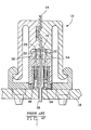
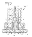
- FIGs 1 and 2 There is shown in Figures 1 and 2 a prior art connector 10, one mating half 12 of which has the conductors of a ribbon cable 14 terminated thereto and the other mating half 16 of which is attached to a printed circuit board 18.
- the signal conductors 22 of the cable 14 are bent to the right and terminated to the terminals 24, the signal conductors 26 are bent to the left and terminated to the terminals 28, and the ground conductors 30 are terminated to the ground bus 32.
- the terminals 24 and 28 mate with the sockets 34 and 36 respectively which are disposed in the connector half 16 of the connector 10, the sockets being electrically connected to the traces of the printed circuit board 18.
- the ground bus 32 mates with a ground receptacle 38 which also is disposed in the connector half 16 and electrically connected to the ground circuit of the printed circuit board 18.
- the ground bus 32 is made of a single sheet of metal folded over to form a double thickness. The two free edges form a V for receiving the ground conductors 30. During assembly, the tips of the V may be pressed toward each other into clenching engagement with the ground conductors 30 and solder flowed throughout the junction to assure good electrical contact.
- U.S. Patent Number 4,747,787 which issued May 31, 1988 to Siwinski and which is incorporated by reference though set forth verbatim herein.
- a serious problem may occur with the termination of the ground conductors 30 to the ground bus 32 of the connector 10. Since these terminations are effectively hidden between two solid pieces of metal, there is virtually no way to visually examine the site to determine the adequacy of the solder connection. Frequently, contamination is lodged within the V portion of the ground plane 32 during manufacturing which interferes with the subsequent soldering operation. Additionally, air pockets may form making it difficult or impossible to flow a sufficient amount of solder to effect a lasting low-resistance connection.
- the present invention overcomes these problems by means of a novel ground bus termination and method of effecting it.
- the present invention sets forth a novel termination of a wire conductor of an electrical cable and method for effecting the termination.
- a plate is provided having an opening formed therein, the opening having two substantially parallel walls. The walls are spaced apart a distance greater than the diameter of the wire conductor.
- a constriction is provided within the opening that mechanically holds and positions a portion of the wire conductor within the opening a distance from each of the walls.
- An electrically conductive material is provided in low-resistance contact with the portion of the wire conductor and both of the walls.
- the ground bus 50 is a plate having a series of equally spaced openings 52 disposed in an edge 54 thereof.
- the openings 52 are formed in a major surface 56 of the plate 50 and may, as in the present example, penetrate through the entire thickness of the plate 50. However, the openings 52 need only penetrate to a depth below the surface 56 preferably equal to an amount slightly greater than the diameter of the ground wire conductor to be terminated.
- a portion of the ribbon cable 14, as best seen in Figure 5, is shown with an end stripped and prepared for terminating.
- every other wire conductor is a ground conductor 30 while the remaining conductors are signal conductors 22 which are bent to the right and signal conductors 26 which are bent to the left, as taught by the '787 patent.
- Each ground conductor has a diameter equal to D, therefore, the depth of the openings 52 is preferably greater than D.
- the openings 52 are formed with substantially parallel walls 60, as shown in Figure 11, having a width WI that is larger than the diameter D of the ground wire conductor 30.
- the openings 52 may be formed in the plate 50 by any suitable means such as stamping or etching.
- the plate 50 is made of an electrically conductive material such as, for example, copper or a copper alloy.
- the openings 52 include a constriction in the form of a pair of mutually opposed projections 62 which project inwardly from the walls 60 so that the distance W2 between them is slightly smaller than the diameter D. While the present case exemplifies two mutually opposed projections 62, more than two such projections may be advantageously used and pairs of such projections may or may not be mutually opposed.
- projections 62 are spaced so that when a ground wire conductor 30 is laterally forced into an opening 52, as will be described in further detail below, the conductor 30 is mechanically held and positioned within the opening so that it is spaced from both walls 60.
- the procedure for assembly of a stripped and prepared ribbon cable 18 to the connector 48 is illustrated in Figures 6 through 11.
- the end of the ribbon cable is prepared is set forth in U.S. Patent Numbers 4,860,447 and 4,860,801 both of which issued on August 29, 1989 to Nicholas et al. and U.S. Patent Number 4,757,845 which issued July 19, 1988 to Sivinski, all of which are incorporated by reference as though set forth verbatim herein.
- the prepared cable and, as shown in Figure 6, includes the stripped signal conductors 22 bent to the right and 26 bent to the left, and the stripped ground conductors 30 which extend in axial alignment with the ribbon cable 14.
- a connector housing 72 as described in the '801 patent, has a longitudinal control slot 74 for receiving the elongate, electrically conductive ground bus 50.
- the housing 72 has a longitudinal central plane extending through the slot 72 and ground hub 50.
- a plurality of parallel apertures 76 are formed in the housing 72 on opposite sides of the control slot 74 for receiving signal contacts 78.
- the housing 72 and ribbon cable 14 are positioned, as shown in Figure 6, so that the ground conductors 30 are slightly to the right of a surface 80 of the ground bus 50.
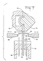
- the fixture 70 is then advanced toward the housing 72 until the ground conductors 50 are immediately adjacent respective openings 52 in the ground bus 50.
- a pair of insertion tools 82 are caused to move toward the ground bus 50, one tool engaging the bus 50 opposite the surface 80 and the other tool engaging the ground conductors 30. Movement continues until the ground conductors 30 are forced into their respective openings 52 so that the projections 62 hold the conductors in position within the openings approximately flush with the surface 80.
- either the fixture 70 or the housing 72 is permitted to move laterally a slight amount to accommodate the lateral movement of the ground conductors 30 toward the control plane of the housing 72.
- the connector housing 72 is then slid along the bus 50 toward the fixture 70 until the signal conductors 22,26 engage V-notches 86 in the ends of the contacts.
- the V-notches 86 and the ground bus 50 in the area adjacent the openings 52, which have been previously coated with a suitable amount of solder, are now exposed to a heat source, not shown.
- the heat source is sufficient to reflow the solder so that a low-resistance contact is made between the signal wires 22,26 and the respective contacts 78 and between the ground conductors 30 and the ground bus 50.
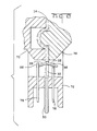
- Figure 9 is a cross-sectional view of a portion of the ground bus 50 taken through one of the openings 52, with a ground conductor 22,26 in place but prior to soldering.
- Figure 10 is a view similar to that of Figure 9 except that the soldering operation is complete. Note then, in Figure 9, the projections 62 hold the conductor 22,26 away from the walls 60 of the opening 52. The purpose of this is to provide sufficient space around the conductor 22,26 to result in a good mechanically strong and low-resistance soldered contact. As will be seen in Figure 10, solder 88 has flowed and adhered to both sides of the conductor and both walls 60 and formed mechanically strong filets therebetween. The assembled connector housing 72 and ribbon cable 14 are then assembled to the remaining connector portions shown in Figure 3 to complete the connector 48 in accordance with the procedures set forth in the '447 patent.
- An important advantage of the present invention is that the openings 52 and their respective constrictions, mechanically hold the ground conductors in position during the soldering operation thereby assuring a strong low-resistance connection. Further, site of each such connection is unobstructed so that a visual inspection may be performed as desired for quality control. Additionally, since the ground bus 50 is substantially flat, it is less subject to collecting contaminants and the forming of air pockets that may interfere with the soldering operation.
Landscapes
- Multi-Conductor Connections (AREA)
- Coupling Device And Connection With Printed Circuit (AREA)
- Details Of Connecting Devices For Male And Female Coupling (AREA)
Abstract
Description
- This invention relates to a connector for coupling the conductors of a cable to tracks of a printed circuit board and, more particularly, to connecting particular ground conductors of the cable to a ground bus within the connector.
- There is shown in Figures 1 and 2 a
prior art connector 10, onemating half 12 of which has the conductors of aribbon cable 14 terminated thereto and theother mating half 16 of which is attached to a printedcircuit board 18. As is seen in Figure 2, thesignal conductors 22 of thecable 14 are bent to the right and terminated to theterminals 24, thesignal conductors 26 are bent to the left and terminated to theterminals 28, and theground conductors 30 are terminated to theground bus 32. Theterminals sockets connector half 16 of theconnector 10, the sockets being electrically connected to the traces of the printedcircuit board 18. Theground bus 32 mates with aground receptacle 38 which also is disposed in theconnector half 16 and electrically connected to the ground circuit of the printedcircuit board 18. As is best seen in Figure 2, theground bus 32 is made of a single sheet of metal folded over to form a double thickness. The two free edges form a V for receiving theground conductors 30. During assembly, the tips of the V may be pressed toward each other into clenching engagement with theground conductors 30 and solder flowed throughout the junction to assure good electrical contact. For a thorough description of theconnector 10, its use, and method of manufacture, please refer to U.S. Patent Number 4,747,787 which issued May 31, 1988 to Siwinski and which is incorporated by reference though set forth verbatim herein. - A serious problem may occur with the termination of the
ground conductors 30 to theground bus 32 of theconnector 10. Since these terminations are effectively hidden between two solid pieces of metal, there is virtually no way to visually examine the site to determine the adequacy of the solder connection. Frequently, contamination is lodged within the V portion of theground plane 32 during manufacturing which interferes with the subsequent soldering operation. Additionally, air pockets may form making it difficult or impossible to flow a sufficient amount of solder to effect a lasting low-resistance connection. - The present invention overcomes these problems by means of a novel ground bus termination and method of effecting it.
- The present invention sets forth a novel termination of a wire conductor of an electrical cable and method for effecting the termination. A plate is provided having an opening formed therein, the opening having two substantially parallel walls. The walls are spaced apart a distance greater than the diameter of the wire conductor. A constriction is provided within the opening that mechanically holds and positions a portion of the wire conductor within the opening a distance from each of the walls. An electrically conductive material is provided in low-resistance contact with the portion of the wire conductor and both of the walls.
- The invention will now be described by way of example with reference to the accompanying drawings in which:
- FIGURE 1 is an isometric view of a prior art connector for terminating the conductors of a ribbon cable and coupling them to traces on a printed circuit board;
- FIGURE 2 is a cross-sectional view of the connector shown in Figure 1;
- FIGURE 3 is a view similar to that of Figure 2 showing a ground bus in accordance with the present invention;
- FIGURE 4 is an isometric view of a ground bus in accordance with teachings of the present invention;
- FIGURE 5 is an isometric view showing the ground bus of Figure 3 in relation to a prepared end of a ribbon cable;
- FIGURE 6, 7 and 8 are cross-sectional views showing the ribbon cable and a portion of the connector in various stages of assembly;
- FIGURE 9 is a cross-sectional view of a portion of the ground bus showing a ground wire conductor in place prior to soldering;
- FIGURE 10 is a view similar to that of Figure 9 after soldering; and
- FIGURE 11 is an enlarged view of a portion of the ground bus shown in Figure 3.
- There is shown in Figure 3, a
connector 48 that is similar to theconnector 10 of Figure 2 with the exception that theground bus 32 is replaced with aground bus 50 in accordance with the teachings of the present invention. As is shown in Figures 4, 11 and 5 theground bus 50 is a plate having a series of equallyspaced openings 52 disposed in anedge 54 thereof. Theopenings 52 are formed in amajor surface 56 of theplate 50 and may, as in the present example, penetrate through the entire thickness of theplate 50. However, theopenings 52 need only penetrate to a depth below thesurface 56 preferably equal to an amount slightly greater than the diameter of the ground wire conductor to be terminated. A portion of theribbon cable 14, as best seen in Figure 5, is shown with an end stripped and prepared for terminating. Note that every other wire conductor is aground conductor 30 while the remaining conductors aresignal conductors 22 which are bent to the right andsignal conductors 26 which are bent to the left, as taught by the '787 patent. Each ground conductor has a diameter equal to D, therefore, the depth of theopenings 52 is preferably greater than D. - The
openings 52 are formed with substantiallyparallel walls 60, as shown in Figure 11, having a width WI that is larger than the diameter D of theground wire conductor 30. Theopenings 52 may be formed in theplate 50 by any suitable means such as stamping or etching. Theplate 50 is made of an electrically conductive material such as, for example, copper or a copper alloy. Theopenings 52 include a constriction in the form of a pair of mutuallyopposed projections 62 which project inwardly from thewalls 60 so that the distance W2 between them is slightly smaller than the diameter D. While the present case exemplifies two mutuallyopposed projections 62, more than two such projections may be advantageously used and pairs of such projections may or may not be mutually opposed. The important requirement of theprojections 62 is that they be spaced so that when aground wire conductor 30 is laterally forced into anopening 52, as will be described in further detail below, theconductor 30 is mechanically held and positioned within the opening so that it is spaced from bothwalls 60. - The procedure for assembly of a stripped and prepared
ribbon cable 18 to theconnector 48 is illustrated in Figures 6 through 11. The end of the ribbon cable is prepared is set forth in U.S. Patent Numbers 4,860,447 and 4,860,801 both of which issued on August 29, 1989 to Nicholas et al. and U.S. Patent Number 4,757,845 which issued July 19, 1988 to Sivinski, all of which are incorporated by reference as though set forth verbatim herein. The prepared cable and, as shown in Figure 6, includes the strippedsignal conductors 22 bent to the right and 26 bent to the left, and the strippedground conductors 30 which extend in axial alignment with theribbon cable 14. The preparedcable 14 is held in afixture 70 in accordance with the teachings of the '447 and '801 patents. A connector housing 72, as described in the '801 patent, has alongitudinal control slot 74 for receiving the elongate, electricallyconductive ground bus 50. Thehousing 72 has a longitudinal central plane extending through theslot 72 andground hub 50. A plurality ofparallel apertures 76 are formed in thehousing 72 on opposite sides of thecontrol slot 74 forreceiving signal contacts 78. Thehousing 72 andribbon cable 14 are positioned, as shown in Figure 6, so that theground conductors 30 are slightly to the right of asurface 80 of theground bus 50. - The
fixture 70 is then advanced toward thehousing 72 until theground conductors 50 are immediately adjacentrespective openings 52 in theground bus 50. A pair ofinsertion tools 82, arranged as shown in Figure 7, are caused to move toward theground bus 50, one tool engaging thebus 50 opposite thesurface 80 and the other tool engaging theground conductors 30. Movement continues until theground conductors 30 are forced into theirrespective openings 52 so that theprojections 62 hold the conductors in position within the openings approximately flush with thesurface 80. During this operation, either thefixture 70 or thehousing 72 is permitted to move laterally a slight amount to accommodate the lateral movement of theground conductors 30 toward the control plane of thehousing 72. - The
connector housing 72 is then slid along thebus 50 toward thefixture 70 until thesignal conductors notches 86 in the ends of the contacts. The V-notches 86 and theground bus 50 in the area adjacent theopenings 52, which have been previously coated with a suitable amount of solder, are now exposed to a heat source, not shown. The heat source is sufficient to reflow the solder so that a low-resistance contact is made between thesignal wires respective contacts 78 and between theground conductors 30 and theground bus 50. - Figure 9 is a cross-sectional view of a portion of the
ground bus 50 taken through one of theopenings 52, with aground conductor projections 62 hold theconductor walls 60 of theopening 52. The purpose of this is to provide sufficient space around theconductor solder 88 has flowed and adhered to both sides of the conductor and bothwalls 60 and formed mechanically strong filets therebetween. The assembled connector housing 72 andribbon cable 14 are then assembled to the remaining connector portions shown in Figure 3 to complete theconnector 48 in accordance with the procedures set forth in the '447 patent. - An important advantage of the present invention is that the
openings 52 and their respective constrictions, mechanically hold the ground conductors in position during the soldering operation thereby assuring a strong low-resistance connection. Further, site of each such connection is unobstructed so that a visual inspection may be performed as desired for quality control. Additionally, since theground bus 50 is substantially flat, it is less subject to collecting contaminants and the forming of air pockets that may interfere with the soldering operation. - While the above description of the present invention included examples of terminating the conductors of ribbon cable to the connector it will be understood that such cable is presented by way of example only and that the teachings of the present invention may be advantageously employed in terminating cables having discrete conductors as well.
Claims (10)
Applications Claiming Priority (2)
| Application Number | Priority Date | Filing Date | Title |
|---|---|---|---|
| US07/558,135 US5074806A (en) | 1990-07-26 | 1990-07-26 | Method and apparatus for coupling a connector to a cable |
| US558135 | 1990-07-26 |
Publications (3)
| Publication Number | Publication Date |
|---|---|
| EP0468512A2 true EP0468512A2 (en) | 1992-01-29 |
| EP0468512A3 EP0468512A3 (en) | 1992-04-22 |
| EP0468512B1 EP0468512B1 (en) | 1997-03-05 |
Family
ID=24228359
Family Applications (1)
| Application Number | Title | Priority Date | Filing Date |
|---|---|---|---|
| EP91112532A Expired - Lifetime EP0468512B1 (en) | 1990-07-26 | 1991-07-25 | Method and apparatus for coupling a connector to a cable |
Country Status (4)
| Country | Link |
|---|---|
| US (1) | US5074806A (en) |
| EP (1) | EP0468512B1 (en) |
| JP (1) | JP3016045B2 (en) |
| DE (1) | DE69124860T2 (en) |
Cited By (3)
| Publication number | Priority date | Publication date | Assignee | Title |
|---|---|---|---|---|
| GB2261328A (en) * | 1991-11-08 | 1993-05-12 | Minnesota Mining & Mfg | Cable grounding connection for an electrical connector |
| EP0565329A2 (en) * | 1992-04-07 | 1993-10-13 | The Whitaker Corporation | Shielded electrical connector |
| AT513004A1 (en) * | 2012-05-16 | 2013-12-15 | Sallaberger | Connectors and ribbon cables with connectors |
Families Citing this family (5)
| Publication number | Priority date | Publication date | Assignee | Title |
|---|---|---|---|---|
| US5575681A (en) * | 1994-12-16 | 1996-11-19 | Itt Corporation | Connector termination to flat cable |
| US6595796B1 (en) | 1997-03-31 | 2003-07-22 | The Whitaker Corporation | Flexible film circuit connector |
| US5924891A (en) * | 1997-12-15 | 1999-07-20 | The Whitaker Corporation | Connector assembly for flat circuitry |
| US5967832A (en) * | 1998-02-23 | 1999-10-19 | 3M Innovative Properties Company | High speed connector assembly |
| CN205029121U (en) * | 2015-09-10 | 2016-02-10 | 番禺得意精密电子工业有限公司 | Cable connecting device and electric connector's combination |
Citations (4)
| Publication number | Priority date | Publication date | Assignee | Title |
|---|---|---|---|---|
| US4225207A (en) * | 1979-03-29 | 1980-09-30 | Akzona Incorporated | Convertible cable-connector assembly |
| US4288917A (en) * | 1978-06-26 | 1981-09-15 | Akzona Incorporated | Method of forming connector-cable with crimped electrical terminations |
| US4824384A (en) * | 1987-03-09 | 1989-04-25 | Amp Incorporated | Electrical cable connector and method of use |
| US4912772A (en) * | 1989-03-06 | 1990-03-27 | International Business Machines Corporation | Connector and circuit package apparatus for pin array circuit module and circuit board |
Family Cites Families (11)
| Publication number | Priority date | Publication date | Assignee | Title |
|---|---|---|---|---|
| DE2525623C3 (en) * | 1975-06-09 | 1978-10-12 | Siemens Ag, 1000 Berlin Und 8000 Muenchen | Connection element for jumper wires |
| US4365856A (en) * | 1980-07-09 | 1982-12-28 | Hirose Electric Co., Ltd. | Electric connector for coaxial ribbon cable |
| US4415216A (en) * | 1981-03-03 | 1983-11-15 | Thomas & Betts Corporation | Connector for mass-ground termination of multiconductor cable |
| US4655515A (en) * | 1985-07-12 | 1987-04-07 | Amp Incorporated | Double row electrical connector |
| US4681382A (en) * | 1985-12-20 | 1987-07-21 | Amp Incorporated | Electrical connector for transmission cable |
| US4692121A (en) * | 1986-07-03 | 1987-09-08 | Amp Incorporated | Dual slot electrical contact and method of making same |
| JPS6380492A (en) * | 1986-09-24 | 1988-04-11 | 京セラエルコ株式会社 | Wiring of connector |
| US4747787A (en) * | 1987-03-09 | 1988-05-31 | Amp Incorporated | Ribbon cable connector |
| US4860801A (en) * | 1988-03-15 | 1989-08-29 | Amp Incorporated | Method and apparatus for bending ribbon cables |
| US4860447A (en) * | 1988-03-15 | 1989-08-29 | Amp Incorporated | Method and apparatus for coupling connectors to ribbon cables |
| US4900279A (en) * | 1989-04-24 | 1990-02-13 | Die Tech, Inc. | Solder terminal |
-
1990
- 1990-07-26 US US07/558,135 patent/US5074806A/en not_active Expired - Lifetime
-
1991
- 1991-07-25 EP EP91112532A patent/EP0468512B1/en not_active Expired - Lifetime
- 1991-07-25 DE DE69124860T patent/DE69124860T2/en not_active Expired - Fee Related
- 1991-07-26 JP JP3208944A patent/JP3016045B2/en not_active Expired - Fee Related
Patent Citations (4)
| Publication number | Priority date | Publication date | Assignee | Title |
|---|---|---|---|---|
| US4288917A (en) * | 1978-06-26 | 1981-09-15 | Akzona Incorporated | Method of forming connector-cable with crimped electrical terminations |
| US4225207A (en) * | 1979-03-29 | 1980-09-30 | Akzona Incorporated | Convertible cable-connector assembly |
| US4824384A (en) * | 1987-03-09 | 1989-04-25 | Amp Incorporated | Electrical cable connector and method of use |
| US4912772A (en) * | 1989-03-06 | 1990-03-27 | International Business Machines Corporation | Connector and circuit package apparatus for pin array circuit module and circuit board |
Cited By (4)
| Publication number | Priority date | Publication date | Assignee | Title |
|---|---|---|---|---|
| GB2261328A (en) * | 1991-11-08 | 1993-05-12 | Minnesota Mining & Mfg | Cable grounding connection for an electrical connector |
| EP0565329A2 (en) * | 1992-04-07 | 1993-10-13 | The Whitaker Corporation | Shielded electrical connector |
| EP0565329A3 (en) * | 1992-04-07 | 1995-04-26 | Whitaker Corp | Shielded electrical connector |
| AT513004A1 (en) * | 2012-05-16 | 2013-12-15 | Sallaberger | Connectors and ribbon cables with connectors |
Also Published As
| Publication number | Publication date |
|---|---|
| JP3016045B2 (en) | 2000-03-06 |
| US5074806A (en) | 1991-12-24 |
| DE69124860T2 (en) | 1997-06-12 |
| EP0468512A3 (en) | 1992-04-22 |
| JPH06318473A (en) | 1994-11-15 |
| EP0468512B1 (en) | 1997-03-05 |
| DE69124860D1 (en) | 1997-04-10 |
Similar Documents
| Publication | Publication Date | Title |
|---|---|---|
| US8758041B2 (en) | Insulation displacement connector (IDC) | |
| US7927144B2 (en) | Electrical connector with interlocking plates | |
| US7997933B2 (en) | Electrical connector system | |
| US4526429A (en) | Compliant pin for solderless termination to a printed wiring board | |
| US4072387A (en) | Multiple conductor connector unit and cable assembly | |
| US4225209A (en) | Electrical connector receptacle | |
| EP0651468B1 (en) | Circuit board and edge-mountable connector therefor, and method of preparing a circuit board edge | |
| US4090667A (en) | Universally programmable shorting plug for an integrated circuit socket | |
| US4418972A (en) | Electrical connector for printed wiring board | |
| US4005921A (en) | Transmission cable connector and termination method | |
| US3855567A (en) | Electrical connector and method for making an electrical circuit | |
| CN107069262B (en) | Electrical connector | |
| US5536182A (en) | Insulation displacement connector | |
| WO2009017509A1 (en) | Electrical termination device | |
| JP2704305B2 (en) | High frequency connector and method of manufacturing the same | |
| US4758168A (en) | Contact device composed of a plug and a corresponding socket | |
| EP0242019A2 (en) | Communications connector | |
| EP0140473A1 (en) | Solderless circuit board conductor and connector assemblies employing same | |
| US5074806A (en) | Method and apparatus for coupling a connector to a cable | |
| US4501464A (en) | Modular connector with improved housing and contact structure | |
| EP0109297B1 (en) | Improvements in electrical contact members and electrical connector assemblies | |
| JP3453630B2 (en) | Coaxial cable connector | |
| US7850489B1 (en) | Electrical connector system | |
| EP0282194B1 (en) | Electrical cable connector | |
| EP0145315A2 (en) | Connecting device for closely spaced conductors and electrical contact terminal therefor |
Legal Events
| Date | Code | Title | Description |
|---|---|---|---|
| PUAI | Public reference made under article 153(3) epc to a published international application that has entered the european phase |
Free format text: ORIGINAL CODE: 0009012 |
|
| AK | Designated contracting states |
Kind code of ref document: A2 Designated state(s): DE FR GB IT NL |
|
| PUAL | Search report despatched |
Free format text: ORIGINAL CODE: 0009013 |
|
| AK | Designated contracting states |
Kind code of ref document: A3 Designated state(s): DE FR GB IT NL |
|
| 17P | Request for examination filed |
Effective date: 19920609 |
|
| RAP1 | Party data changed (applicant data changed or rights of an application transferred) |
Owner name: THE WHITAKER CORPORATION |
|
| 17Q | First examination report despatched |
Effective date: 19940610 |
|
| GRAG | Despatch of communication of intention to grant |
Free format text: ORIGINAL CODE: EPIDOS AGRA |
|
| GRAH | Despatch of communication of intention to grant a patent |
Free format text: ORIGINAL CODE: EPIDOS IGRA |
|
| GRAH | Despatch of communication of intention to grant a patent |
Free format text: ORIGINAL CODE: EPIDOS IGRA |
|
| GRAA | (expected) grant |
Free format text: ORIGINAL CODE: 0009210 |
|
| AK | Designated contracting states |
Kind code of ref document: B1 Designated state(s): DE FR GB IT NL |
|
| ITF | It: translation for a ep patent filed | ||
| REF | Corresponds to: |
Ref document number: 69124860 Country of ref document: DE Date of ref document: 19970410 |
|
| ET | Fr: translation filed | ||
| PLBE | No opposition filed within time limit |
Free format text: ORIGINAL CODE: 0009261 |
|
| STAA | Information on the status of an ep patent application or granted ep patent |
Free format text: STATUS: NO OPPOSITION FILED WITHIN TIME LIMIT |
|
| 26N | No opposition filed | ||
| PGFP | Annual fee paid to national office [announced via postgrant information from national office to epo] |
Ref country code: NL Payment date: 19990630 Year of fee payment: 9 |
|
| PG25 | Lapsed in a contracting state [announced via postgrant information from national office to epo] |
Ref country code: NL Free format text: LAPSE BECAUSE OF NON-PAYMENT OF DUE FEES Effective date: 20010201 |
|
| NLV4 | Nl: lapsed or anulled due to non-payment of the annual fee |
Effective date: 20010201 |
|
| REG | Reference to a national code |
Ref country code: GB Ref legal event code: IF02 |
|
| PGFP | Annual fee paid to national office [announced via postgrant information from national office to epo] |
Ref country code: FR Payment date: 20060717 Year of fee payment: 16 |
|
| PGFP | Annual fee paid to national office [announced via postgrant information from national office to epo] |
Ref country code: GB Payment date: 20060726 Year of fee payment: 16 |
|
| PGFP | Annual fee paid to national office [announced via postgrant information from national office to epo] |
Ref country code: IT Payment date: 20060731 Year of fee payment: 16 |
|
| PGFP | Annual fee paid to national office [announced via postgrant information from national office to epo] |
Ref country code: DE Payment date: 20060831 Year of fee payment: 16 |
|
| GBPC | Gb: european patent ceased through non-payment of renewal fee |
Effective date: 20070725 |
|
| PG25 | Lapsed in a contracting state [announced via postgrant information from national office to epo] |
Ref country code: DE Free format text: LAPSE BECAUSE OF NON-PAYMENT OF DUE FEES Effective date: 20080201 |
|
| PG25 | Lapsed in a contracting state [announced via postgrant information from national office to epo] |
Ref country code: GB Free format text: LAPSE BECAUSE OF NON-PAYMENT OF DUE FEES Effective date: 20070725 |
|
| REG | Reference to a national code |
Ref country code: FR Ref legal event code: ST Effective date: 20080331 |
|
| PG25 | Lapsed in a contracting state [announced via postgrant information from national office to epo] |
Ref country code: FR Free format text: LAPSE BECAUSE OF NON-PAYMENT OF DUE FEES Effective date: 20070731 |
|
| PG25 | Lapsed in a contracting state [announced via postgrant information from national office to epo] |
Ref country code: IT Free format text: LAPSE BECAUSE OF NON-PAYMENT OF DUE FEES Effective date: 20070725 |