EP0468255A2 - Linear image sensor of the contact type - Google Patents
Linear image sensor of the contact type Download PDFInfo
- Publication number
- EP0468255A2 EP0468255A2 EP91111233A EP91111233A EP0468255A2 EP 0468255 A2 EP0468255 A2 EP 0468255A2 EP 91111233 A EP91111233 A EP 91111233A EP 91111233 A EP91111233 A EP 91111233A EP 0468255 A2 EP0468255 A2 EP 0468255A2
- Authority
- EP
- European Patent Office
- Prior art keywords
- image sensor
- contact type
- pitch
- picture elements
- chip
- Prior art date
- Legal status (The legal status is an assumption and is not a legal conclusion. Google has not performed a legal analysis and makes no representation as to the accuracy of the status listed.)
- Withdrawn
Links
- 239000004065 semiconductor Substances 0.000 description 3
- 238000009792 diffusion process Methods 0.000 description 2
- 239000000758 substrate Substances 0.000 description 2
- 238000010276 construction Methods 0.000 description 1
- 230000000694 effects Effects 0.000 description 1
Images
Classifications
-
- H—ELECTRICITY
- H04—ELECTRIC COMMUNICATION TECHNIQUE
- H04N—PICTORIAL COMMUNICATION, e.g. TELEVISION
- H04N1/00—Scanning, transmission or reproduction of documents or the like, e.g. facsimile transmission; Details thereof
- H04N1/04—Scanning arrangements, i.e. arrangements for the displacement of active reading or reproducing elements relative to the original or reproducing medium, or vice versa
- H04N1/19—Scanning arrangements, i.e. arrangements for the displacement of active reading or reproducing elements relative to the original or reproducing medium, or vice versa using multi-element arrays
- H04N1/1903—Arrangements for enabling electronic abutment of lines or areas independently scanned by different elements of an array or by different arrays
-
- H—ELECTRICITY
- H01—ELECTRIC ELEMENTS
- H01L—SEMICONDUCTOR DEVICES NOT COVERED BY CLASS H10
- H01L27/00—Devices consisting of a plurality of semiconductor or other solid-state components formed in or on a common substrate
- H01L27/14—Devices consisting of a plurality of semiconductor or other solid-state components formed in or on a common substrate including semiconductor components sensitive to infrared radiation, light, electromagnetic radiation of shorter wavelength or corpuscular radiation and specially adapted either for the conversion of the energy of such radiation into electrical energy or for the control of electrical energy by such radiation
- H01L27/144—Devices controlled by radiation
- H01L27/146—Imager structures
-
- H—ELECTRICITY
- H04—ELECTRIC COMMUNICATION TECHNIQUE
- H04N—PICTORIAL COMMUNICATION, e.g. TELEVISION
- H04N1/00—Scanning, transmission or reproduction of documents or the like, e.g. facsimile transmission; Details thereof
- H04N1/04—Scanning arrangements, i.e. arrangements for the displacement of active reading or reproducing elements relative to the original or reproducing medium, or vice versa
- H04N1/19—Scanning arrangements, i.e. arrangements for the displacement of active reading or reproducing elements relative to the original or reproducing medium, or vice versa using multi-element arrays
- H04N1/191—Scanning arrangements, i.e. arrangements for the displacement of active reading or reproducing elements relative to the original or reproducing medium, or vice versa using multi-element arrays the array comprising a one-dimensional array, or a combination of one-dimensional arrays, or a substantially one-dimensional array, e.g. an array of staggered elements
- H04N1/192—Simultaneously or substantially simultaneously scanning picture elements on one main scanning line
- H04N1/193—Simultaneously or substantially simultaneously scanning picture elements on one main scanning line using electrically scanned linear arrays, e.g. linear CCD arrays
- H04N1/1934—Combination of arrays
Abstract
Description
- The present invention relates to a linear image sensor of the contact type used in an image scanner and a facsimile machine etc.
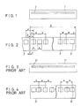
- There is known an image sensor of the contact type comprised of a plurality of image sensor chips arranged linearly with one another. Fig. 3 is a plan view of an example of such contact type linear image sensor. A plurality of
image sensor chips 21 are arranged linearly on abase plate 11. Fig. 4 shows a plan view of oneimage sensor chip 21. Thechip 21 provided with a linear array ofpicture elements 31 arranged such that an end element is spaced an interval b from an inner adjacent element and the remaining intermediate elements are spaced an interval a from each other. The end interval b is set smaller than the intermediate interval a. Further, the intermediate interval a is set exactly identical to a given standard reading pitch of the sensor in the horizontal or main scanning direction. Theimage sensor chip 21 is comprised of a semiconductor IC, and eachpicture element 31 has a light receiving region composed of a diffusion layer having one conductivity type opposite to that of a semiconductor substrate of the IC chip. The end interval b is set smaller than the intermediate interval a in order to compensate for a gap between adjacentimage sensor chips 21 to maintain overall regularlity of the standard reading pitch. - If an
end element 31 were disposed too closely to an edge of the chip with the regular interval a, there would be caused a drawback that a leak current would flow excessively between the light receiving diffusion layer and the semiconductor substrate. - However, the above noted conventional image sensor of the contact type has a drawback that an output level of the end picture element is varied relative to the remaining intermediate elements. Namely, since the end interval b between the end element and the inner adjacent element is set smaller than the intermediate interval a of the remaining elements, an electrode pattern layout around the end element is different from those around the remaining elements. Stated otherwise, there is caused a parastic capacitance variation between a signal electrode pattern around an individual picture element and a light receiving region, thereby generating nonuniform outputs. It would be quite difficult to compensate for such variation provisionally by pattern design.
- An object of the present invention is to eliminate the drawback of the prior art to provide an improved image sensor of the contact type having uniform output performance. In order to achieve the above noted object, according to the invention, an end picture element is spaced from an inner adjacent element a pitch identical to a given constant intermediate pitch a' of the remaining elements, which is set slightly smaller than a standard reading pitch a of the horizontal or main scanning direction so that the electrode pattern layout is commonly set around every picture element, thereby ensuring uniform output performance of the contact type image sensor.
- In the contact type image sensor constructed as described above, the end picture element has therearound a pattern layout which is identical to those around the remaining elements so that the end element can produce an output in uniform manner as the remaining elements. Consequently, there can be obtained the contact type image sensor having uniform output performance.
- Further, the contact pitch a' may be set to satisfy the relation n(a - a') < a where n denotes a number of picture elements contained in one image sensor chip along the horizontal scanning direction, in order to limit a total dimensional error of the picture element array within a scale of one standard reading pitch to substantially eliminate horizontal distortion of a read image relative to an original image.
-
- Fig. 1 is a plan view showing one embodiment of the inventive image sensor of the contact type;
- Fig. 2 is a plan view showing an image sensor chip contained in the inventive image sensor of the contact type;
- Fig. 3 is a plan view of the conventional image sensor of the contact type; and
- Fig. 4 is a plan view of an image sensor chip contained in the conventional image sensor of the contact type.
- Hereinafter, one embodiment of the invention will be described in conjunction with the drawings. Fig. 1 is a plan view of the inventive image sensor of the contact type. A plurality of
image sensor chips 2 are arranged linearly on abase plate 1. Adjacentimage sensor chips 2 are disposed closely at a gap f less than several tens am. - Fig. 2 shows an enlarged plan view of one
image sensor chip 2. Thechip 2 has an array of n pieces ofpicture elements 3 arranged linearly in main or horizontal scanning direction. Thepicture elements 3 are disposed a given constant interval or pitch a' throughout the entire of the array. The pitch a' is set slightly smaller than a standard reading pitch a of the horizontal scanning direction, which is calculated by dividing a span of the liner sensor by a total number of picture elements. Further, local lead electrode patterns are designed identically in and around all thepicture elements 3 including end ones, thereby avoiding nonuniform variation of outputs at a particular element within the sameimage sensor chip 2, for example, at opposite end elements. Such variation would be caused by difference in local lead electrode pattern layouts. - Moreover, the linear arrangement pitch a' is preferably set to satisfy the following relation (f):

- By such arrangement, a total positional error of the picture elements can be limited below an order of one standard pitch a within one chip. For example, if each sensor image chip array has a 16 dots/mm of image reading resolution and n=128 number of picture elements, the standard reading pitch a is calculated to 1 mm/16 = 62.5µm and the arrangement pitch a' should be no less than 62.012µm according
- On the other hand, a reading span of 128 dots is calculated to 128 - 16 = 8mm, hence the chip length I should be less than 8mm to leave a gap between adjacent chips. Though depending on mounting accuracy of chips, the gap f between adjacent chips is, for example, estimated
r to accurately mou nt linearly the chips in matching with the given standard reading pitch. - As indicated in Fig. 2, a distance c from a center of the end picture element to the chip edge is represented by the following relation (2):

3 µm. Accordingly, a sufficient ligh t recei ving area can be obtained effectively. In addition, an interval a" of apposed end picture elements between adjacent chips is set to a" = 2c + f = 113.3µm. This value is greaterth an the standard reading pitch a = 62.5µm by about 80 %. Generally, a dimensional error of more or less one picture element order does not effect quality of a reproduced image in case of 16 dots/mm of the resolution. A side form above, an actual arrangement pitch may be locally widened exceptionally at one or more intermediate spots, relative to the constant pitch value a' in view of optimum and efficient lead pattern layout. However, in such case, the constant pitch a' is maintained almost all of the picture elements including end ones, thereby maintaining uniform quality of a reproduced image. The present invention can be applied not only to an image sensor having a single line of picture elements, but also to those having multiple lines of picture elements. - As described above, according to the present invention, there can be obtained a linear image sensor of the contact type having uniform output performance with simplified construction.
Claims (2)
Applications Claiming Priority (2)
| Application Number | Priority Date | Filing Date | Title |
|---|---|---|---|
| JP2198286A JP3013189B2 (en) | 1990-07-26 | 1990-07-26 | Contact image sensor |
| JP198286/90 | 1990-07-26 |
Publications (2)
| Publication Number | Publication Date |
|---|---|
| EP0468255A2 true EP0468255A2 (en) | 1992-01-29 |
| EP0468255A3 EP0468255A3 (en) | 1992-03-11 |
Family
ID=16388598
Family Applications (1)
| Application Number | Title | Priority Date | Filing Date |
|---|---|---|---|
| EP19910111233 Withdrawn EP0468255A3 (en) | 1990-07-26 | 1991-07-05 | Linear image sensor of the contact type |
Country Status (6)
| Country | Link |
|---|---|
| US (1) | US5619345A (en) |
| EP (1) | EP0468255A3 (en) |
| JP (1) | JP3013189B2 (en) |
| KR (1) | KR100212030B1 (en) |
| CA (1) | CA2047930A1 (en) |
| TW (1) | TW198768B (en) |
Cited By (5)
| Publication number | Priority date | Publication date | Assignee | Title |
|---|---|---|---|---|
| DE4317945A1 (en) * | 1993-03-22 | 1994-09-29 | Paul Dr Debbage | Method and device for investigating an object |
| DE4325724A1 (en) * | 1993-07-30 | 1995-02-02 | Paul Dr Debbage | Device and method for examining an object and for affecting the object |
| EP0657938A1 (en) * | 1993-12-06 | 1995-06-14 | Minnesota Mining And Manufacturing Company | Solid state radiation detection panel having tiled photosensitive detectors arranged to minimize edge effects between tiles |
| EP0975143A2 (en) * | 1998-07-22 | 2000-01-26 | Hewlett-Packard Company | Multi-segment linear photosensor assembly |
| EP1091558A1 (en) * | 1998-01-30 | 2001-04-11 | Rohm Co., Ltd. | Image sensor chip and image reading device provided with it |
Families Citing this family (6)
| Publication number | Priority date | Publication date | Assignee | Title |
|---|---|---|---|---|
| US6556315B1 (en) | 1999-07-30 | 2003-04-29 | Hewlett-Packard Company | Digital image scanner with compensation for misalignment of photosensor array segments |
| JP2003143381A (en) * | 2001-08-22 | 2003-05-16 | Canon Inc | Image processing apparatus |
| JP2003115984A (en) * | 2001-10-05 | 2003-04-18 | Seiko Instruments Inc | Image reader |
| JP3829853B2 (en) * | 2004-03-31 | 2006-10-04 | 三菱電機株式会社 | Image sensor |
| JP4179329B2 (en) | 2006-03-17 | 2008-11-12 | セイコーエプソン株式会社 | Line sensor chip, line sensor, image information reading device, facsimile, scanner and copying machine |
| JP6822010B2 (en) * | 2016-08-29 | 2021-01-27 | セイコーエプソン株式会社 | Scanner and image data generation method |
Citations (4)
| Publication number | Priority date | Publication date | Assignee | Title |
|---|---|---|---|---|
| FR2110763A5 (en) * | 1970-10-29 | 1972-06-02 | Comp Generale Electricite | |
| JPS57157680A (en) * | 1981-03-25 | 1982-09-29 | Toshiba Corp | Line sensor for picture reading |
| JPS5957563A (en) * | 1982-09-27 | 1984-04-03 | Toshiba Corp | Solid-state linear image sensor |
| JPS6149463A (en) * | 1984-08-17 | 1986-03-11 | Matsushita Electronics Corp | One-dimensional image sensor |
Family Cites Families (4)
| Publication number | Priority date | Publication date | Assignee | Title |
|---|---|---|---|---|
| US4652743A (en) * | 1984-11-30 | 1987-03-24 | Brother Kogyo Kabushiki Kaisha | Optical image-reading apparatus |
| US4748516A (en) * | 1985-03-15 | 1988-05-31 | Brother Kogyo Kabushiki Kaisha | Input/output device for image reading and printing |
| US4692812A (en) * | 1985-03-26 | 1987-09-08 | Kabushiki Kaisha Toshiba | Picture image reader |
| JPH0287869A (en) * | 1988-09-26 | 1990-03-28 | Ricoh Co Ltd | Zigzag array multichip type image sensor |
-
1990
- 1990-07-26 JP JP2198286A patent/JP3013189B2/en not_active Expired - Lifetime
-
1991
- 1991-07-02 TW TW080105140A patent/TW198768B/zh not_active IP Right Cessation
- 1991-07-05 EP EP19910111233 patent/EP0468255A3/en not_active Withdrawn
- 1991-07-15 KR KR1019910012069A patent/KR100212030B1/en not_active IP Right Cessation
- 1991-07-16 US US07/731,741 patent/US5619345A/en not_active Expired - Lifetime
- 1991-07-25 CA CA002047930A patent/CA2047930A1/en not_active Abandoned
Patent Citations (4)
| Publication number | Priority date | Publication date | Assignee | Title |
|---|---|---|---|---|
| FR2110763A5 (en) * | 1970-10-29 | 1972-06-02 | Comp Generale Electricite | |
| JPS57157680A (en) * | 1981-03-25 | 1982-09-29 | Toshiba Corp | Line sensor for picture reading |
| JPS5957563A (en) * | 1982-09-27 | 1984-04-03 | Toshiba Corp | Solid-state linear image sensor |
| JPS6149463A (en) * | 1984-08-17 | 1986-03-11 | Matsushita Electronics Corp | One-dimensional image sensor |
Non-Patent Citations (4)
| Title |
|---|
| IEEE INTERNATIONAL SOLID-STATE CIRCUITS CONFERENCE, 32ND CONF. vol. 28, February 1985, CORAL GABLES, FLORIDA, USA TADASHI AOKI ET AL. (PAGE 102-103, 319): 'A COLLINEAR 3-CHIP IMAGE SENSOR' * |
| PATENT ABSTRACTS OF JAPAN vol. 10, no. 209 (E-421)(2265) 22 July 1986 & JP-A-61 049 463 ( MATSUSHITA ELECTRONICS CORP ) * |
| PATENT ABSTRACTS OF JAPAN vol. 6, no. 259 (E-149)17 December 1982 & JP-A-57 157 680 ( TOKYO SHIBAURA DENKI KK ) * |
| PATENT ABSTRACTS OF JAPAN vol. 8, no. 155 (E-265)(1592) 19 July 1984 & JP-A-59 057 563 ( TOSHIBA KK ) * |
Cited By (7)
| Publication number | Priority date | Publication date | Assignee | Title |
|---|---|---|---|---|
| DE4317945A1 (en) * | 1993-03-22 | 1994-09-29 | Paul Dr Debbage | Method and device for investigating an object |
| DE4325724A1 (en) * | 1993-07-30 | 1995-02-02 | Paul Dr Debbage | Device and method for examining an object and for affecting the object |
| EP0657938A1 (en) * | 1993-12-06 | 1995-06-14 | Minnesota Mining And Manufacturing Company | Solid state radiation detection panel having tiled photosensitive detectors arranged to minimize edge effects between tiles |
| EP1091558A1 (en) * | 1998-01-30 | 2001-04-11 | Rohm Co., Ltd. | Image sensor chip and image reading device provided with it |
| EP1091558A4 (en) * | 1998-01-30 | 2003-01-15 | Rohm Co Ltd | Image sensor chip and image reading device provided with it |
| EP0975143A2 (en) * | 1998-07-22 | 2000-01-26 | Hewlett-Packard Company | Multi-segment linear photosensor assembly |
| EP0975143A3 (en) * | 1998-07-22 | 2000-12-20 | Hewlett-Packard Company | Multi-segment linear photosensor assembly |
Also Published As
| Publication number | Publication date |
|---|---|
| KR100212030B1 (en) | 1999-08-02 |
| TW198768B (en) | 1993-01-21 |
| KR920003535A (en) | 1992-02-29 |
| EP0468255A3 (en) | 1992-03-11 |
| CA2047930A1 (en) | 1992-01-27 |
| US5619345A (en) | 1997-04-08 |
| JPH0483462A (en) | 1992-03-17 |
| JP3013189B2 (en) | 2000-02-28 |
Similar Documents
| Publication | Publication Date | Title |
|---|---|---|
| EP0468255A2 (en) | Linear image sensor of the contact type | |
| US6163036A (en) | Light emitting element module with a parallelogram-shaped chip and a staggered chip array | |
| EP0319907B1 (en) | Light emitting diode array chip and method of fabricating the same | |
| US5552828A (en) | Geometries for photosites in a photosensitive silicon chip | |
| EP0986103B1 (en) | Light emitting element module and printer head using the same | |
| US4775895A (en) | Modular image sensor structure | |
| US6952289B1 (en) | Integrated image reading/writing head, and image processing apparatus incorporating the same | |
| US6448995B1 (en) | Image read/write head, and image processing apparatus incorporating the same | |
| EP0872892A2 (en) | LED array and printer for an electrophotographic printer with said LED array | |
| US5305021A (en) | Thermal head | |
| JP3771368B2 (en) | Image sensor chip arrangement method and image reading apparatus using the arrangement method | |
| EP0544607A2 (en) | Thermal recording head and method of manufacturing the same | |
| EP0908953A1 (en) | Light emitting element module and chip | |
| US5337474A (en) | Process for fabricating electronic devices and image sensor | |
| JP2001339574A (en) | Image reader | |
| EP0507366B1 (en) | LED exposure head | |
| JPH0211193B2 (en) | ||
| EP0449477A1 (en) | Colour image sensor | |
| JPH11331492A (en) | Multi-chip mounting unmagnified image sensor and multi-chip mounted led print head | |
| JPS621357A (en) | Reader | |
| JPS60218968A (en) | Optical reader | |
| JPH08184736A (en) | Optical device | |
| JPS60218967A (en) | Optical reader | |
| JPH09283807A (en) | Light detecting and emitting element module | |
| JPH0575788A (en) | Multi-chip type image sensor |
Legal Events
| Date | Code | Title | Description |
|---|---|---|---|
| PUAI | Public reference made under article 153(3) epc to a published international application that has entered the european phase |
Free format text: ORIGINAL CODE: 0009012 |
|
| PUAL | Search report despatched |
Free format text: ORIGINAL CODE: 0009013 |
|
| AK | Designated contracting states |
Kind code of ref document: A2 Designated state(s): DE FR GB IT |
|
| AK | Designated contracting states |
Kind code of ref document: A3 Designated state(s): DE FR GB IT |
|
| 17P | Request for examination filed |
Effective date: 19920813 |
|
| 17Q | First examination report despatched |
Effective date: 19950207 |
|
| STAA | Information on the status of an ep patent application or granted ep patent |
Free format text: STATUS: THE APPLICATION IS DEEMED TO BE WITHDRAWN |
|
| 18D | Application deemed to be withdrawn |
Effective date: 19950620 |