EP0467085B1 - Driving circuit for brushless D.C. motor - Google Patents
Driving circuit for brushless D.C. motor Download PDFInfo
- Publication number
- EP0467085B1 EP0467085B1 EP91110041A EP91110041A EP0467085B1 EP 0467085 B1 EP0467085 B1 EP 0467085B1 EP 91110041 A EP91110041 A EP 91110041A EP 91110041 A EP91110041 A EP 91110041A EP 0467085 B1 EP0467085 B1 EP 0467085B1
- Authority
- EP
- European Patent Office
- Prior art keywords
- circuit
- output
- stage
- driving circuit
- control circuit
- Prior art date
- Legal status (The legal status is an assumption and is not a legal conclusion. Google has not performed a legal analysis and makes no representation as to the accuracy of the status listed.)
- Expired - Lifetime
Links
Images


Classifications
-
- H—ELECTRICITY
- H02—GENERATION; CONVERSION OR DISTRIBUTION OF ELECTRIC POWER
- H02P—CONTROL OR REGULATION OF ELECTRIC MOTORS, ELECTRIC GENERATORS OR DYNAMO-ELECTRIC CONVERTERS; CONTROLLING TRANSFORMERS, REACTORS OR CHOKE COILS
- H02P6/00—Arrangements for controlling synchronous motors or other dynamo-electric motors using electronic commutation dependent on the rotor position; Electronic commutators therefor
- H02P6/14—Electronic commutators
Definitions
- the invention relates to a driver circuit for a brushless DC motor according to the preamble of claim 1.
- Such a driver circuit is already known from WO 87/02528 for brushless DC motors, which contains all circuit elements for direct control of the motor windings in the form of an integrated circuit and manages with a minimum of external components, namely a Hall IC as a rotor position transmitter and a single capacitor as Timing element in a pulse generator of the control circuit.
- this known control circuit it is possible to control or regulate the power supplied to the DC motor as a function of a setpoint or a reference variable, so that it can be adapted to the needs. So it is e.g. It is possible to use the brushless DC motor as a fan motor to control the cooling capacity of the fan depending on the heat generated by an electronic device, i.e. the fan runs slowly and generates little noise when the heat is generated, while the fan runs faster and the amount of cooling air increases when the heat is generated feeds.
- This known control circuit including output stages is operated by means of a low DC operating voltage of e.g. 12V supply, which is normally taken from the power supply of the electronic device.
- the driver circuit has a power output stage, a control circuit, a power supply device and intermediate driver stages.
- the power output stage is only switched on by the control circuit when the driver stage is switched off.
- the amplitude of the rectangular output signal of the driver stages is not determined by the amplitude of the control signal at the output of the control circuit, but by the resistance value of a PTC resistor.
- the power output stages are connected to an operating voltage between 8 volts and 30 volts.
- the present invention is based on the object of proposing a driver circuit for a brushless DC motor, in particular a fan motor, which permits optimum control of the power output stage even in the case of large motors and causes little noise.
- Such a driver circuit has the main advantage that an existing control circuit for lower powers can be used for flexible control or regulation of the direct current motor and the increase in power can be achieved with the corresponding additional power output stages with only a few components.
- the required auxiliary power supply only needs to have a relatively low output because the output stages of the existing control circuit are only operated with a relatively low output current.
- control circuit delivers ramp-shaped output pulses, with a pulse within each commutation phase, which have the form of symmetrical triangular pulses of variable amplitude at lower output powers and pass into the form of trapezoidal pulses of variable width with further increase.
- the use of such a control circuit for controlling the power output stages has the great advantage that the entire driver circuit operates at low powers in analog operation with relatively flat rising and falling edges of the output pulses, so that the DC motor causes only little noise during operation. If the output power increases, on the other hand, the driver circuit operates in analog / switch mode with trapezoidal output pulses with a better efficiency, so that the power losses in the power output stages do not increase too much.
- the somewhat higher noise of the motor that occurs hardly disturbs in the case of fan operation, since the noise of the fan also increases.
- the triangular or trapezoidal pulses of the driver circuit are preferably symmetrical within the commutation phases of the motor in order to achieve the highest possible efficiency.
- the auxiliary power supply is preferably designed as an integrated circuit which uses a clocked switch and a charging capacitor to derive a screened and regulated DC voltage from the AC network.
- Such a circuit has the advantage that it does not require a mains transformer and still has a relatively high degree of efficiency.
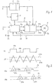
- a rectifier circuit 2 is connected to an alternating current network 6 of, for example, 230 V, which generates an output direct voltage 10 of, for example, 200-300 V from this alternating voltage without using a transformer.
- This DC output voltage 10 is fed to a power output stage 3, which has a brushless DC motor 5 directly via output lines 14a and 14b feeds.
- the power output stages 3 are controlled by means of a control circuit 4 via output lines 13a and 13b.
- This control circuit 4 including a downstream intermediate driver stage 3a, is fed from the AC network 6 by means of an auxiliary power supply 1.
- the auxiliary power supply 1 generates a low DC output voltage of e.g. 12V, for which the control circuit 4 and the intermediate driver stage 3a are designed.
- the power to be applied by the auxiliary power supply 1 is relatively low, since the power for driving the brushless DC motor 5 is provided directly from the power supply 6 by the rectifier circuit 2.
- the rectifier circuit 2 also contains a monitoring circuit 2 a, which ensures inrush current limitation and overcurrent limitation in a known manner.
- the control circuit 4 is designed in the form of an integrated circuit, as is shown, for example, in the PCT publication WO 87/02528 already mentioned.
- This control circuit contains all components for controlling the motor windings of a brushless DC motor of lower power via output lines 13a and 13b, which are connected to internal output stages of the control circuit 4.
- the pulse 11a determines the commutation phase for one of the motor windings, while the pulse pause 11b defines the commutation phase for the other motor winding.
- a triangular voltage 20 (see FIG. 2) is derived from the output signals 11 of the rotor position sensor 5a, the pulses of which lie symmetrically to the commutation phases 11a and 11b of the rotor position sensor 5a.
- the width of the triangular pulses - regardless of the speed of the motor 5 - corresponds approximately to the width of the commutation phase 11a or 11b, specifically by evaluating the voltage 12 proportional to the speed of the motor 5 and in conjunction with an external capacitor 8 as a timing element . Details of this circuit can be found in the PCT publication WO 87/02528 already mentioned.
- the control circuit 4 is supplied with a target value 7 or a reference variable which determines a threshold value 21a or 21b. If the target value 7 is low, there is, for example, a threshold value at the level of the dashed line 21a.
- the control circuit 4 has the effect that the portion of the triangular voltage 20 exceeding this threshold is output by the respective output stage of the control circuit 4 as an output signal 13a or 13b, as shown in FIG. 2 for the two output lines 13a and 13b.
- the triangular pulses 22a and 22b belong to the threshold value 21a. If the target value 7 is increased, the threshold value is lowered in the direction of the lower value 21b.
- Triangular pulses 23a and 23b of higher amplitude arise per se. The peaks of these triangular pulses do not become effective, however, since the output stages within the control circuit 4 and the power output stages 3 are already saturated. The triangular pulses of higher amplitude thus become trapezoidal pulses 23a and 23b. 2, this threshold is shown by the dashed line 24, from which the output stage transistors pass into saturation.
- the control circuit 4 thus has the effect that triangular pulses 22a and 22b of variable amplitude are generated on their output lines 13a and 13b in the respective commutation phase 11a and 11b, these pulses going into trapezoidal shape 23a and 23b at higher values. It can be seen that both the triangular pulses 22a and 22b and the trapezoidal pulses 23a and 23b lie symmetrically within the commutation phases 11a and 11b, respectively, so that there is an optimum efficiency for the direct current motor 15.
- the control circuit 4 may also contain a control circuit in order to regulate the output signals 13a, 13b or 14a, 14b depending on the setpoint 7 and a feedback speed voltage 12.
- the output stages in the control circuit 4 are normal suitable for direct operation of a DC motor with lower power.
- intermediate driver stages 3a are provided between the control circuit 4 and the power output stages 3, which effect the corresponding signal adaptation and also ensure that the output current in the lines 14a and 14b are directly proportional to the output signals 13a and 13b of the control circuit 4.
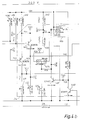
- FIG. 3 shows a power supply part
- FIG. 4 shows the speed control and the power output stages as well as intermediate driver stages and a monitoring circuit.
- the DC output voltage on line 10 is smoothed by capacitor 311, to which a discharge resistor 312 is connected in parallel.
- the mains voltage which can be tapped off at the resistor 304 is also applied to the input of the auxiliary power supply 1 via series resistors 314, 315. From there, a further capacitor 318 is connected to ground potential.
- the auxiliary power supply is also directly connected to ground potential with one or more lines.
- the smoothing capacitors 319 and 320 also connect the auxiliary power supply 1 to ground potential.
- the auxiliary power supply unit generates a voltage of approximately 12 volts on the output line 9. This is monitored by a Zener diode 316. In FIG.
- the high DC supply voltage is supplied to the stator coils of the DC motor 5 via connection point L1 via the monitoring circuit 2a (here implemented as a PTC resistor). These are connected to the associated field-effect transistors 428 and 427 of the output stage 3 by means of the line 14a and 14b.
- the control signals for the transistors 427 and 428 are derived, as already mentioned above, from the output signals of the rotor position transmitter 5a, which draws its supply voltage from the control circuit 4 and also returns its useful signals there via the line 11.
- the delta voltage is available at capacitor 419, while the actual speed value can be tapped at capacitor 8.
- the output signals of the control circuit 4 are applied to the bases of the transistors 423 and 424 via lines 13a and 13b, the bases being provided with a positive bias voltage via the resistors 408 and 409, respectively.
- Transistors 423, 424 are PNP transistors whose emitters are connected to the low supply voltage of approximately 12 volts via a common series resistor 410. Both transistors are connected to ground with a collector resistance (411.412) of approximately 3 kilohms each. The signal that can be tapped at the collectors is in each case given directly to the non-inverting inputs of the current control stages 425 or 426.
- the operational amplifiers of the current control stages 425 and 426 receive their supply voltage via the output of a restart circuit 555, which ensures a reliable restart of the motor in the event of a prolonged overload or blocking of the motor 5.
- a restart circuit 555 which ensures a reliable restart of the motor in the event of a prolonged overload or blocking of the motor 5.
- the current control stages 425 and 426 receive supply voltage for about one second, whereupon their supply voltage is switched off again for about four seconds. This gives the monitoring circuit 2a (PTC resistor) the opportunity to cool down sufficiently and to provide a nominal starting current.
- the operation of the restart circuit is based on the fact that the control circuit 4, based on the transistor 438, gives a speed-proportional trigger signal (two pulses per motor expansion), which, after further inversion via the transistor 437, means that the capacitor 435 is not appreciably via the series resistor 432 and the right arm of the double diode 434 can be charged. If these trigger pulses are absent, capacitor 435 charges up, so that the collector of transistor 437 is at an elevated potential after a few seconds and causes the restart circuit 555 to oscillate via the trigger input. This is achieved in that a discharge output of the restart circuit 555 can discharge the capacitor 435 via a discharge resistor 433 and the left arm of the double diode 434.
- the discharge takes about four times longer than the charging of the capacitor 435.
- the current regulating stages 425 and 426 are thus provided with supply voltage in an approximately 5-second cycle for about one second, and until the control circuit 4 again gives trigger pulses to the base of the transistor 438, so that the capacitor 435 can be kept discharged at all times.
Description
Die Erfindung betrifft eine Treiberschaltung für einen bürstenlosen Gleichstrommotor nach dem Oberbegriff des Anspruchs 1.The invention relates to a driver circuit for a brushless DC motor according to the preamble of
Eine solche Treiberschaltung ist aus WO 87/02528 bereits für bürstenlose Gleichstrommotoren bekannt, die in Form einer integrierten Schaltung alle Schaltungselemente zur direkten Ansteuerung der Motorwicklungen enthält und mit einem Minimum von externen Bauelementen auskommt, nämlich einem Hall-IC als Rotorpositionsgeber und einem einzigen Kondensator als Zeitglied in einem Impulsformgenerator der Steuerschaltung.Such a driver circuit is already known from WO 87/02528 for brushless DC motors, which contains all circuit elements for direct control of the motor windings in the form of an integrated circuit and manages with a minimum of external components, namely a Hall IC as a rotor position transmitter and a single capacitor as Timing element in a pulse generator of the control circuit.
Mit dieser bekannten Steuerschaltung ist es möglich, die dem Gleichstrommotor zugeführte Leistung abhängig von einem Sollwert oder einer Führungsgröße zu steuern oder zu regeln, so daß diese den Bedürfnissen angepaßt werden kann. So ist es z.B. möglich, bei der Verwendung des bürstenlosen Gleichstrommotors als Lüftermotor die Kühlleistung des Lüfters abhängig von der Wärmeentwicklung eines elektronischen Gerätes zu steuern, d.h., bei niedriger Wärmeentwicklung läuft der Lüfter langsam und entwickelt wenig Geräusch, während bei höherer Wärmeentwicklung der Lüfter schneller läuft und eine größere Kühlluftmenge zuführt. Diese bekannte Steuerschaltung einschließlich Endstufen wird mittels einer niedrigen Betriebsgleichspannung von z.B. 12V versorgt, die normalerweise dem sowieso vorhandenen Netzteil des elektronischen Gerätes entnommen wird.With this known control circuit, it is possible to control or regulate the power supplied to the DC motor as a function of a setpoint or a reference variable, so that it can be adapted to the needs. So it is e.g. It is possible to use the brushless DC motor as a fan motor to control the cooling capacity of the fan depending on the heat generated by an electronic device, i.e. the fan runs slowly and generates little noise when the heat is generated, while the fan runs faster and the amount of cooling air increases when the heat is generated feeds. This known control circuit including output stages is operated by means of a low DC operating voltage of e.g. 12V supply, which is normally taken from the power supply of the electronic device.
Der Leistungsfähigkeit eines solchen bürstenlosen Gleichstrommotors einschließlich Steuerschaltung und Endstufen sind jedoch Grenzen gesetzt, die insbesondere von der in einer integrierten Schaltung maximal zulässigen Verlustleistung bestimnt werden. Darüber hinaus ist die aus dem Netzteil eines vorhandenen elektronischen Gerätes lieferbare Gleichstromleistung ebenfalls begrenzt. Deshalb werden normalerweise größere Lüfter direkt aus dem Wechselstromnetz gespeist, um das Netzteil des elektronischen Gerätes nicht zu überlasten. Ein solcher Lüfter ist dann jedoch in seiner Leistung normalerweise nicht regelbar, so daß auch bei niedriger, erforderlicher Kühlleistung der Lüfter mit voller Leistung und verhältnismäßig hohem Geräusch weiterläuft.However, the performance of such a brushless DC motor including control circuit and output stages are limited, in particular are determined by the maximum permissible power loss in an integrated circuit. In addition, the direct current power available from the power supply of an existing electronic device is also limited. For this reason, larger fans are usually fed directly from the AC network so as not to overload the power supply of the electronic device. However, such a fan cannot normally be regulated in its output, so that the fan continues to run at full output and relatively high noise even when the cooling power required is low.
Eine weitere Steuerschaltung für einen bürstenlosen Gleichstrommotor ist in EP-A-0 318 938 beschrieben. Zwischen die Steuerschaltung und die Leistungsendstufe sind Optokoppler geschaltet, die ausschließlich zur Potentialtrennung von Leistungsendstufe und Steuerschaltung dienen. Obwohl bei dieser bekannten Schaltungsanordnung bereits eine getrennte Stromversorgung der Leistungsendstufe und der Steuerschaltung vorgesehen ist, zeichnet sich diese Treiberschaltung durch eine verhältnismäßig einfache Regelung der Lüfterleistung aus. Die Leistungsregelung des Lüfters wird nämlich ausschließlich durch ein pulsweitenmoduliertes Ein- und Ausschalten des Ausgangssignales der Steuerschaltung bewirkt.Another control circuit for a brushless DC motor is described in EP-
Eine weitere Steuerschaltung für einen kollektorlosen Gleichstrommotor ist in EP-A-0 084 156 beschrieben. Die Treiberschaltung weist eine Leistungsendstufe, eine Steuerschaltung, eine Stromversorgungseinrichtung sowie Zwischentreiberstufen auf. Die Leistungsendstufe wird durch die Steuerschaltung nur dann eingeschaltet, wenn die Treiberstufe abgeschaltet ist. Zudem wird die Amplitude des rechteckförmigen Ausgangssignales der Treiberstufen nicht durch die Amplitude des Steuersignales am Ausgang der Steuerschaltung bestimmt, sondern vom Widerstandswert eines PTC-Widerstandes. Die Leistungsendstufen sind bei dieser bekannten Schaltungsanordnung an eine Betriebsspannung zwischen 8 Volt und 30 Volt angeschlossen.Another control circuit for a collectorless DC motor is described in EP-A-0 084 156. The driver circuit has a power output stage, a control circuit, a power supply device and intermediate driver stages. The power output stage is only switched on by the control circuit when the driver stage is switched off. In addition, the amplitude of the rectangular output signal of the driver stages is not determined by the amplitude of the control signal at the output of the control circuit, but by the resistance value of a PTC resistor. In this known circuit arrangement, the power output stages are connected to an operating voltage between 8 volts and 30 volts.
Der vorliegenden Erfindung liegt die Aufgabe zugrunde, eine Treiberschaltung für einen bürstenlosen Gleichstromnotor, insbesondere einen Lüftermotor, vorzuschlagen, die eine optimale Ansteuerung der Leistungsendstufe auch bei großen Motoren erlaubt und eine geringe Geräuschentwicklung verursacht.The present invention is based on the object of proposing a driver circuit for a brushless DC motor, in particular a fan motor, which permits optimum control of the power output stage even in the case of large motors and causes little noise.
Diese Aufgabe wird durch eine Treiberschaltung mit den Merkmalen des Anspruchs 1 gelöst.This object is achieved by a driver circuit with the features of
Eine solche Treiberschaltung hat den wesentlichen Vorteil, daß eine bereits vorhandene Steuerschaltung für niedrigere Leistungen zur flexiblen Steuerung bzw. Regelung des Gleichstrommotors eingesetzt werden kann und die Leistungserhöhung durch die entsprechenden zusätzlichen Leistungsendstufen mit nur wenigen Bauelementen realisiert werden kann. Das erforderliche Hilfsnetzteil braucht nur eine verhältnismäßig niedrige Leistung zu haben, weil die Endstufen der vorhandenen Steuerschaltung nur mit verhältnismäßig niedrigem Ausgangsstrom betrieben werden.Such a driver circuit has the main advantage that an existing control circuit for lower powers can be used for flexible control or regulation of the direct current motor and the increase in power can be achieved with the corresponding additional power output stages with only a few components. The required auxiliary power supply only needs to have a relatively low output because the output stages of the existing control circuit are only operated with a relatively low output current.
Weiterbildungen der Erfindung sind Gegenstand der Unteransprüche.Developments of the invention are the subject of the dependent claims.
Eine vorteilhafte Ausgestaltung der Erfindung sieht vor , daß die Steuerschaltung rampenförmige Ausgangsimpulse liefert, wobei innerhalb jeder Kommutierungsphase ein Impuls liegt, die bei niedrigeren Ausgangsleistungen die Form symmetrischer Dreiecksimpulse variabler Amplitude haben und bei weiterem Ansteigen in die Form von Trapezimpulsen variabler Breite übergehen. Durch die Verwendung einer solchen Steuerschaltung zur Ansteuerung der Leistungsendstufen ergibt sich der große Vorteil, daß die gesamte Treiberschaltung bei niedrigen Leistungen im Analog-Betrieb mit verhältnismäßig flachen Anstiegs- und Abfallflanken der Ausgangsimpulse arbeitet, so daß der Gleichstrommotor im Betrieb nur geringe Geräusche verursacht. Bei einem Ansteigen der Ausgangsleistung dagegen, arbeitet die Treiberschaltung im Analog-/Schalterbetrieb mit trapezförmigen Ausgangsimpulsen bei einem besseren Wirkungsgrad, so daß die Verlustleistungen in den Leistungsendstufen nicht zu stark ansteigen. Die dabei auftretenden etwas höheren Geräusche des Motors stören im Falle eines Lüfterbetriebes kaum, da die Geräusche des Lüfters ebenfalls ansteigen. Die Dreiecks- bzw. Trapezimpulse der Treiberschaltung liegen vorzugsweise symmetrisch innerhalb der Kommutierungsphasen des Motors, um zu einem möglichst hohen Wirkungsgrad zu kommen.An advantageous embodiment of the invention provides that the control circuit delivers ramp-shaped output pulses, with a pulse within each commutation phase, which have the form of symmetrical triangular pulses of variable amplitude at lower output powers and pass into the form of trapezoidal pulses of variable width with further increase. The use of such a control circuit for controlling the power output stages has the great advantage that the entire driver circuit operates at low powers in analog operation with relatively flat rising and falling edges of the output pulses, so that the DC motor causes only little noise during operation. If the output power increases, on the other hand, the driver circuit operates in analog / switch mode with trapezoidal output pulses with a better efficiency, so that the power losses in the power output stages do not increase too much. The somewhat higher noise of the motor that occurs hardly disturbs in the case of fan operation, since the noise of the fan also increases. The triangular or trapezoidal pulses of the driver circuit are preferably symmetrical within the commutation phases of the motor in order to achieve the highest possible efficiency.
Das Hilfsnetzteil ist vorzugsweise als integrierte Schaltung ausgebildet, die mittels eines getakteten Schalters und eines Ladekondensators aus dem Wechselstromnetz eine gesiebte und geregelte Gleichspannung ableitet. Eine solche Schaltung hat den Vorteil, daß sie ohne einen Netztransformator auskommt und trotzdem einen verhältnismäßig hohen Wirkungsgrad aufweist.The auxiliary power supply is preferably designed as an integrated circuit which uses a clocked switch and a charging capacitor to derive a screened and regulated DC voltage from the AC network. Such a circuit has the advantage that it does not require a mains transformer and still has a relatively high degree of efficiency.
Die Erfindung wird nachfolgend anhand eines Ausführungsbeispiels unter Bezug auf die beigefügten Zeichnungen näher erläutert.The invention is explained in more detail below using an exemplary embodiment with reference to the accompanying drawings.
Es zeigen:
- Fig. 1
- das Blockschaltbild der erfindungsgemäßen Treiberschaltung;
- Fig. 2
- ein Impulsdiagramm für die verschiedenen Impulszüge der Treiberschaltung nach Fig. 1;
- Fig. 3
- ein Stromversorgungsteil;
- Fig. 4
- die Drehzahlregelungs- und die Leistungsendstufen.
- Fig. 1
- the block diagram of the driver circuit according to the invention;
- Fig. 2
- a timing diagram for the various pulse trains of the driver circuit of FIG. 1;
- Fig. 3
- a power supply part;
- Fig. 4
- the speed control and power output stages.
An ein Wechselstromnetz 6 von z.B. 230V ist eine Gleichrichterschaltung 2 angeschlossen, die ohne Verwendung eines Transformators aus dieser Wechselspannung eine Ausgangsgleichspannung 10 von z.B. 200 - 300 V erzeugt. Diese Ausgangsgleichspannung 10 wird einer Leistungsendstufe 3 zugeleitet, die direkt über Ausgangsleitungen 14a und 14b einen bürstenlosen Gleichstrommotor 5 speist.A
Die Ansteuerung der Leistungsendstufen 3 erfolgt mittels einer Steuerschaltung 4 über Ausgangsleitungen 13a und 13b. Diese Steuerschaltung 4, einschließlich einer nachgeschalteteten Zwischentreiberstufe 3a wird mittels eines Hilfsnetzteils 1 aus dem Wechselstromnetz 6 gespeist. Das Hilfsnetzteil 1 erzeugt an seinem Ausgang 9 eine niedrige Ausgangsgleichspannung von z.B. 12V, für die die Steuerschaltung 4 und die Zwischentreiberstufe 3a ausgelegt sind. Die von dem Hilfsnetzteil 1 aufzubringende Leistung ist verhältnismäßig gering, da die Leistung für den Antrieb des bürstenlosen Gleichstrommotors 5 durch die Gleichrichterschaltung 2 direkt aus dem Netz 6 bereitgestellt wird.The
Der Gleichrichterschaltung 2 enthält noch eine Überwachungsschaltung 2a, die in bekannter Weise für eine Einschaltstrombegrenzung und Überstrombegrenzung sorgt.The
Nachdem die Stromversorgung der einzelnen Einheiten der Treiberschaltung mittels einer direkt an das Netz 6 angeschlossenen Gleichrichterschaltung 2 und mittels eines zusätzlichen Hilfsnetzteils 1 beschrieben wurde, soll nun die Funktion der Treiberschaltung in Verbindung mit der speziellen Steuerschaltung 4 erläutert werden:After the power supply of the individual units of the driver circuit has been described by means of a
Die Steuerschaltung 4 ist in der Form einer integrierten Schaltung ausgebildet, wie sie z.B. in der bereits genannten PCT-Druckschrift WO 87/02528 dargestellt ist. Diese Steuerschaltung enthält alle Bauelemente zur Ansteuerung der Motorwicklungen eines bürstenlosen Gleichstrommotors geringerer Leistung über Ausgangsleitungen 13a und 13b, die an interne Endstufen der Steuerschaltung 4 angeschlossen sind. Ein Rotorpositionsgeber 5a des Motors 5, vorzugsweise als Hall-IC ausgebildet, liefert über die Leitung 11 Rechteckimpulse 11a, 11b, wie in Fig. 2 gezeigt ist. Der Impuls 11a bestimmt hierbei die Kommutierungsphase für eine der Motorwicklungen, während die Impulspause 11b die Kommutierungsphase für die andere Motorwicklung definiert. Aus den Motorwicklungen werden außerdem, in bekannter Weise, Spannungen ausgekoppelt, die der Drehzahl des Motors 5 proportional sind. Diese gelangen über eine Leitung 12 in die Steuerschaltung 4. Von den Ausgangssignalen 11 des Rotorpositionsgebers 5a wird eine Dreiecksspannung 20 (siehe Fig. 2) abgeleitet, deren Impulse symmetrisch zu den Kommutierungsphasen 11a bzw. 11b des Rotorpositionsgebers 5a liegen. Die Breite der Dreiecksimpulse entspricht - unabhängig von der Drehzahl des Motors 5 - etwa der Breite der Kommutierungsphase 11a bzw. 11b, und zwar wird dies unter Auswertung der der Drehzahl des Motors 5 proportionalen Spannung 12 und in Verbindung mit einem externen Kondensator 8 als Zeitglied erreicht. Einzelheiten dieser Schaltung sind der bereits genannten PCT-Druckschrift WO 87/02528 zu entnehmen.The
Der Steuerschaltung 4 wird ein Sollwert 7 bzw. eine Führungsgröße zugeleitet, die einen Schwellwert 21a bzw. 21b bestimmt. Ist der Sollwert 7 gering, so liegt z.B. ein Schwellwert in der Höhe der gestrichelten Linie 21a vor. Die Steuerschaltung 4 bewirkt, daß der diese Schwelle übersteigende Anteil der Dreiecksspannung 20 von der jeweiligen Endstufe der Steuerschaltung 4 als Ausgangssignal 13a bzw. 13b ausgegeben wird, wie es Fig. 2 für die beiden Ausgangsleitungen 13a bzw. 13b zeigt. Die Dreiecksimpulse 22a und 22b gehören zu dem Schwellwert 21a. Wird der Sollwert 7 erhöht, so wird der Schwellwert in Richtung auf den niedrigeren Wert 21b erniedrigt. Der diesen Schwellwert 21b übersteigende Anteil der Dreiecksspannung 20 ist nunmehr größer, wie aus den Impulszügen 13a bzw. 13b der Fig. 2 hervorgeht. Es entstehen hierbei an sich Dreiecksimpulse 23a bzw. 23b von höherer Amplitude. Die Spitzen dieser Dreiecksimpulse werden jedoch nicht wirksam, da die Endstufen innerhalb der Steuerschaltung 4 bzw. die Leistungsendstufen 3 sich bereits in der Sättigung befinden. Aus den Dreiecksimpulsen höherer Amplitude werden also trapezförmige Impulse 23a bzw. 23b. In Fig. 2 ist durch die gestrichelte Linie 24 diese Schwelle eingezeichnet, von der aus die Endstufentransistoren in die Sättigung übergehen.The
Die Steuerschaltung 4 bewirkt also, daß an ihren Ausgangsleitungen 13a bzw. 13b in der jeweiligen Kommutierungsphase 11a bzw. 11b Dreiecksimpulse 22a bzw. 22b variabler Amplitude erzeugt werden, wobei bei höheren Werten diese Impulse in Trapezform 23a bzw. 23b übergehen. Es ist zu erkennen, daß sowohl die Dreiecksimpulse 22a und 22b als auch die Trapezimpulse 23a und 23b symmetrisch innerhalb der Kommutierungsphasen lla bzw. 11b liegen, so daß sich ein optimaler Wirkungsgrad für den Gleichstrommotor 15 ergibt.The
Die Steuerschaltung 4 enthält ggfs. auch eine Regelschaltung, um die Ausgangssignale 13a, 13b bzw. 14a, 14b abhängig von dem Sollwert 7 und einer rückgeführten Drehzahlspannung 12 zu regeln.The
Die Endstufen in der Steuerschaltung 4 sind normalerweise für den direkten Betrieb eines Gleichstrommotors mit geringerer Leistung geeignet. Um über die Leistungsendstufen 3 die Motorwicklungen mit höherer Leistung direkt proportional den Ausgangssignalen 13a bzw. 13b anzusteuern, sind zwischen der Steuerschaltung 4 und den Leistungsendstufen 3 Zwischentreiberstufen 3a vorgesehen, die die entsprechende Signalanpassung bewirken und außerdem dafür sorgen, daß der Ausgangsstrom in den Leitungen 14a und 14b direkt proportional den Ausgangssignalen 13a und 13b der Steuerschaltung 4 sind.The output stages in the
Die zusammengehörenden Figuren 3 und 4 stellen die beste Ausführungsform dar und geben im Vergleich zu Figur 1 zusätzliche Einzelheiten wieder. Figur 3 stellt einen Stromversorgungsteil dar, während in Figur 4 die Drehzahlregelungs- und die Leistungsendstufen wiedergegeben sind sowie Zwischentreiberstufen und eine Überwachungsschaltung.Figures 3 and 4, which belong together, represent the best embodiment and provide additional details compared to Figure 1. FIG. 3 shows a power supply part, while FIG. 4 shows the speed control and the power output stages as well as intermediate driver stages and a monitoring circuit.
In Figur 3 werden neben den Eingangsklemmen für das Wechselstromnetz 6 die Ausgangsklemmen L1 für 310 Volt Gleichspannung gezeigt, L2 für 12 Volt Gleichspannung, während L3 den Masseanschluß darstellt. Darüberhinaus existieren eine Anzahl an Testpunkten TP, wie sie zur Überprüfung der Schaltung nützlich sind. Die Netzspannung wird zunächst über ein Sicherungselement 305 gegen Kurzschlüsse abgesichert. Eine LC-Kombination bestehend aus der Induktivität 304 und den Kondensatoren 306, 307 sorgt im Zusammenspiel mit einem Varistor 308 für die Begrenzung von Überspannungsimpulsen sowie die EµV-Störunterdrückung. Die Netzschaltung wird sodann mit der Gleichrichterschaltung 2 gleichgerichtet und über einen Vorwiderstand 32 (NTC-Widerstand) auf die Leitung 10 bzw. L1 gegeben. Die zugehörige Masseleitung ist mit den Buchstaben GND gekennzeichnet und führt auf die Ausgangsklemme L3. Die Ausgangsgleichspannung auf der Leitung 10 wird durch den Kondensator 311 geglättet, dem ein Entladewiderstand 312 parallelgeschaltet ist. Die am Widerstand 304 abgreifbare Netzspannung wird weiterhin über Vorwiderstände 314, 315 auf den Eingang des Hilfsnetzteils 1 gelegt. Von dort ist ein weiterer Kondensator 318 gegen Massepotential geschaltet. Das Hilfsnetzteil ist mit einer oder mehreren Leitungen ebenfalls direkt mit Massepotential verbunden. Die Glättungskondensatoren 319 und 320 verbinden das Hilfsnetzteil 1 ebenfalls mit Massepotential. An der Ausgangsleitung 9 erzeugt das Hilfsnetzteil eine Spannung von etwa 12 Volt. Diese wird überwacht durch eine Z-Diode 316. -In Figur 4 wird die hohe Versorgungsgleichspannung über Anschlußpunkt L1 über die Überwachungsschaltung 2a (hier ausgeführt als PTC-Widerstand) den Statorspulen des Gleichstrommotors 5 zugeführt. Diese sind mittels der Leitung 14a bzw. 14b an die zugehörigen Feldeffekttransistoren 428 bzw. 427 der Endstufe 3 angeschlossen. Die Ansteuersignele für die Transistoren 427 und 428 leiten sich ab wie bereits oben erwähnt von den Ausgangssignalen des Rotorpositionsgebers 5a, welcher seine Versorgungsspannung aus der Steuerschaltung 4 bezieht und ebenfalls seine Nutzsignale über die Leitung 11 dorthin zurückgibt. Am Kondensator 419 steht die Dreieckspannung zur Verfügung, während am Kondensator 8 der DrehzahlIstwert abgegriffen werden kann. Die Ausgangssignale der Steuerschaltung 4 werden über Leitungen 13a und 13b auf die Basen der Transistoren 423 bzw. 424 gegeben, wobei die Basen über die Widerstände 408 bzw. 409 mit einer positiven Vorspannung versehen werden. Die Transistoren 423, 424 sind PNP-Transistoren, deren Emitter über einen gemeinsamen Vorwiderstand 410 mit der niedrigen Versorgungsspannung von etwa 12 Volt verbunden sind. Beide Transistoren sind mit jeweils einem Kollektorwiderstand (411,412) von etwa 3 Kiloohm gegen Masse geschaltet. Das an den Kollektoren abgreifbare Signal wird jeweils direkt auf die nicht-invertierenden Eingänge der Stromregelstufen 425 bzw. 426 gegeben. Diese bestehen aus Operationsverstärkern, deren Ausgangssignal zum einen direkt auf die Gates der Endstufentransistoren 427 und 428 geleitet wird, zum anderen über Rückkopplungswiderstände von etwa 33 Kiloohm jeweils auf den invertierenden Eingang zurückgeführt wird. Die invertierenden Eingänge fühlen des weiteren jeweils über einen Vorwiderstand 416, 417 von jeweils etwa 3 Kiloohm eine Spannung am Strommeßwiderstand 415 ab, die dem Motorstrom proportional ist. Auf diese Weise wird sichergestellt, daß die Endtransistoren 427 und 428 nach Maßgabe der Ausgangssignale auf Leitungen 13a und 13b leitfähig gemacht werden. Die Operationsverstärker der Stromregelstufen 425 und 426 erhalten ihre Versorgungsspannung über den Ausgang einer Wiederanlaufschaltung 555, die im Falle einer länger andauernden Überlast bzw. Blockieren des Motors 5 für einen zuverlässigen Wiederanlauf des Motors sorgt. Hierzu ist vorgesehen, daß in einem solchen Überlastfalle die Stromregelstufen 425 und 426 etwa eine Sekunde lang Versorgungsspannung erhalten, worauf für etwa vier Sekunden deren Versorgungsspannung wieder abgeschaltet wird. Dies gibt der Überwachungsschaltung 2a (PTC-Widerstand) Gelegenheit, sich genügend abzukühlen und einen Nominalanlaufstrom bereitzustellen. Die Wirkungsweise der Wideranlaufschaltung beruht darauf, daß die Steuerschaltung 4 auf die Basis des Transistors 438 ein drehzahlproportionales Trigger-Signal gibt (zwei Impulse pro Motorumdehung), welches nach weiterer Invertierung über den Transistor 437 dazu führt, daß der Kondensator 435 nicht nennenswert über den Vorwiderstand 432 und den rechten Arm der Doppeldiode 434 aufgeladen werden kann. Sofern diese Trigger-Pulse ausbleiben, lädt sich Kondensator 435 auf, so daß der Kollektor des Transistors 437 nach einigen Sekunden auf einem erhöhten Potential liegt und über den Trigger-Eingang der Wiederanlaufschaltung 555 diese in Oszillation versetzt. Dieses wird dadurch erreicht, daß ein Entladeausgang der Wiederanlaufschaltung 555 über Entladewiderstand 433 und linken Arm der Doppeldiode 434 den Kondensator 435 entladen kann. Da der Widerstand 433 hoch-ohmiger ist als Aufladewiderstand 432, dauert die Entladung etwa viermal länger als die Aufladung des Kondensators 435. Die Stromregelstufen 425 und 426 werden also in einem ca. 5-Sekunden-Rhythmus jeweils für etwa eine Sekunde mit Versorgungsspannung versehen, und zwar so lange bis nach Wiederanlauf des Motors 5 die Steuerschaltung 4 erneut Trigger-Impulse auf die Basis des Transistors 438 gibt, so daß der Kondensator 435 ständig entladen gehalten werden kann.In Figure 3, in addition to the input terminals for the
Es versteht sich, daß die beschriebene Wiederaralaufschaltung auch mit anderen Vorrichtungen betrieben werden kann, welche durch einen PCT-Widerstand geschützt sind und welche im Normalfall eine Mindestanzahl an Impulsen pro Zeiteinheit bereitstellen, wie z. B. Schaltnetzteilen.It is understood that the re-activation described can also be operated with other devices which are protected by a PCT resistor and which are normally provide a minimum number of pulses per unit of time, e.g. B. Switching power supplies.
Claims (15)
- A driving circuit for a brushless direct current motor with:- at least one final power output stage (3) for motor windings of the direct current motor (5);- a control circuit (4) for operating the final power output stage (3) with triangular or trapezoidal output signals (13a, 13b) which can be adjusted by a sensor device (5a) in the light of commutating phases and as determined by a desired value or a guide variable (7);- a power supply means (1, 2, 2a) for supplying power to the final power output stage (3) with a rectified operating voltage (10) and for supplying power to the control circuit (4);characterised by the features:- of an intermediate driver stage (3a) incorporated between the final power output stage (3) and the control circuit (4) by which output currents (14a, 14b) of the final power output stage (3) are triangular or trapezoidal and can be regulated in proportion to the triangular or trapezoidal output signals (13a, 13b) of the control circuit (4) and- the power supply means (1, 2, 2a) provides, for supplying power to the control circuit (4), a rectified operating voltage (9) which is lower in comparison with the operating voltage (10) of the final power output stage (3), whereby the final power output stage (3), without using a transformer, is connected to terminals of an alternating current network (6) via a rectifying circuit (2), an auxiliary mains unit (1) is provided which is connected to the terminals of the alternating current network (6) and makes available the lower operating voltage (9) for the control circuit (4) and the intermediate driver stage (3a).
- A driving circuit according to Claim 1, characterised in that the intermediate driver stage (3a) couples the control circuit (4) galvanically to the final power output stage (3).
- A driving circuit according to one of Claims 1 to 2, characterised in that the brushless direct current motor (5) is a fan motor with a rotor position transmitter (5a) serving as the sensor means.
- A driving circuit according to Claim 3, characterised in that the control circuit (4) fixes commutation phases of the fan motor as a function of an output signal (11) from the rotor position transmitter (5a).
- A driving circuit according to one of Claims 1 to 4, characterised in that the output signals (13a, 13b) for operating the final power output stage (3) in their amplitude and/or duration are adjustable by the control circuit (4) .
- A driving circuit according to one of Claims 3 to 5, characterised in that the control circuit (4) is constructed as an integrated circuit and contains the following units:- a feed circuit for supplying current to the rotor position transmitter (5a),- a circuit for establishing the commutation phases of the motor windings as a function of the output signals from the rotor position transmitter (5a),- a pulse-forming circuit for controlling or regulating the amplitude and/or duration of the output signals for the individual motor windings as a function of a desired value (7) or of a guide variable,- output stages to make output signals available to the motor windings.
- A driving circuit according to one of Claims 1 to 6, characterised in that the output signals (13a, 13b) provided by the control circuit (4) are pulses whereby within each commutation phase (11a, 11b) there is a pulse which, for a lesser output power, has the form of a symmetrical triangular pulse (22a, 22b) of variable amplitude and which can, upon a further rise, merge into the form of a trapezoidal pulse (23a, 23b) of variable width.
- A driving circuit according to Claim 7, characterised in that the triangular or trapezoidal pulses are located symmetrically within the commutation phases (11a, 11b).
- A driving circuit according to one of Claims 1 to 8, characterised in that the auxiliary mains unit (1) is an integrated circuit which, by means of a clocked switch and a charging capacitor, derives a filtered and regulated direct current voltage from the alternating current network (6).
- A driving circuit according to one of Claims 1 to 9, characterised in that the rectifier circuit (2) for the final power output stage (3) contains a monitoring circuit (2a) for limiting the connection current and limiting the over-voltage current.
- A driving circuit according to one of Claims 1 to 10, characterised in that a restart circuit is provided which delivers a separate supply voltage to the intermediate driver stage (3a), the separate supply voltage retaining either a nominal value in so far as the motor is in its regular operating mode or the separate supply voltage is supplied intermittently to the intermediate driver stage (3a) if the motor is blocked or overloaded.
- A driving circuit according to Claim 11, characterised in that the restart circuit has a sequence of trigger pulses applied to it, the output signal from the restart circuit having a predefined voltage lever in so far as the trigger pulses are at a higher frequency than the predetermined limit frequency and the output signal of the restart circuit is at a different predefined voltage level in so far as the trigger pulses have a lower frequency than a predetermined limit frequency, whereby the restart circuit comprises a time-control component (555), a charging resistor (432), a discharging resistor (433), a capacitor (435), decoupling diodes (434), a discharger (437) and an amplifier (438).
- A driving circuit according to one of Claims 1 to 12, characterised in that the intermediate driver stage (3a) comprises for each output signal (13a, 13b) from the control circuit (4) a transistorised amplifier stage (423, 424) in emitter circuit with a current control stage (425, 426) on the downstream side, an output from the current control stage (425, 426) being coupled to a control input of an associated final power output stage (3).
- A driving circuit according to Claim 3, characterised in that the current control stage (425, 426) is a feedback operational amplifier of which the non-inverting input (+) is connected to an output of the emitter circuit of the transistorised amplifier (423, 424) of which the inverting input (-) is connected to the output of the operational amplifier via a feedback resistor and the output of which is coupled to the control input of the associated final power output stage (3).
- A driving circuit according to Claim 14, characterised in that between the reference potential and the non-inverting input (+) of the operational amplifier (425, 426) there is a collector resistance which acts as a current measuring resistor (415, 416).
Applications Claiming Priority (2)
| Application Number | Priority Date | Filing Date | Title |
|---|---|---|---|
| DE4019338 | 1990-06-18 | ||
| DE4019338A DE4019338A1 (en) | 1990-06-18 | 1990-06-18 | DRIVER CIRCUIT FOR A BRUSHLESS DC MOTOR |
Publications (2)
| Publication Number | Publication Date |
|---|---|
| EP0467085A1 EP0467085A1 (en) | 1992-01-22 |
| EP0467085B1 true EP0467085B1 (en) | 1997-01-08 |
Family
ID=6408576
Family Applications (1)
| Application Number | Title | Priority Date | Filing Date |
|---|---|---|---|
| EP91110041A Expired - Lifetime EP0467085B1 (en) | 1990-06-18 | 1991-06-18 | Driving circuit for brushless D.C. motor |
Country Status (2)
| Country | Link |
|---|---|
| EP (1) | EP0467085B1 (en) |
| DE (2) | DE4019338A1 (en) |
Families Citing this family (10)
| Publication number | Priority date | Publication date | Assignee | Title |
|---|---|---|---|---|
| DE4310260C1 (en) * | 1993-03-30 | 1994-09-08 | Bosch Gmbh Robert | Electronic control device for an electronically commutated direct-current motor (DC motor) |
| DE59405829D1 (en) * | 1993-09-15 | 1998-06-04 | Papst Motoren Gmbh & Co Kg | Arrangement with a commutatorless DC motor commutated via a semiconductor arrangement |
| DE4432530A1 (en) * | 1994-09-13 | 1996-03-14 | Bosch Gmbh Robert | Circuit and method for driving a brushless DC motor |
| DE29780375U1 (en) * | 1996-06-07 | 2000-03-23 | Papst Motoren Gmbh & Co Kg | Arrangement with an electronically commutated motor |
| DE59705198D1 (en) | 1996-06-07 | 2001-12-06 | Papst Motoren Gmbh & Co Kg | ARRANGEMENT WITH AN ELECTRONICALLY COMMUTED MOTOR |
| DE19631517A1 (en) * | 1996-08-03 | 1998-02-05 | Wacker Werke Kg | Variable-speed, hand-held power tool driven by an electric motor that can be connected to single-phase alternating current |
| EP0963034A1 (en) * | 1998-06-05 | 1999-12-08 | Hsin-Mao Hsieh | Drive circuit with signal detection capability for a DC brushless fan motor |
| DE20105050U1 (en) * | 2000-05-27 | 2001-06-28 | Papst Motoren Gmbh & Co Kg | Motor arrangement |
| DE10150448A1 (en) * | 2001-10-12 | 2003-04-30 | Conti Temic Microelectronic | Controlling electronically commutated motor involves reducing current flow angle to minimum value in low speed range with increasing speed, and increasing control transistor drive |
| ITMI20081600A1 (en) * | 2008-09-09 | 2010-03-10 | Cross Technology S R L | ACTUATOR-SENSOR SYSTEM |
Citations (1)
| Publication number | Priority date | Publication date | Assignee | Title |
|---|---|---|---|---|
| EP0084156A1 (en) * | 1981-12-23 | 1983-07-27 | Papst-Motoren GmbH & Co. KG | Collectorless D.C. motor |
Family Cites Families (3)
| Publication number | Priority date | Publication date | Assignee | Title |
|---|---|---|---|---|
| US4052650A (en) * | 1972-07-26 | 1977-10-04 | Danfoss A/S | Starting device for a single-phase motor |
| DE3537403C2 (en) * | 1985-10-21 | 1995-06-01 | Papst Motoren Gmbh & Co Kg | Brushless DC motor with or for a fan |
| US4827196A (en) * | 1987-12-03 | 1989-05-02 | E. I. Du Pont De Nemours And Company | Motor control arrangement |
-
1990
- 1990-06-18 DE DE4019338A patent/DE4019338A1/en not_active Withdrawn
-
1991
- 1991-06-18 EP EP91110041A patent/EP0467085B1/en not_active Expired - Lifetime
- 1991-06-18 DE DE59108461T patent/DE59108461D1/en not_active Expired - Fee Related
Patent Citations (1)
| Publication number | Priority date | Publication date | Assignee | Title |
|---|---|---|---|---|
| EP0084156A1 (en) * | 1981-12-23 | 1983-07-27 | Papst-Motoren GmbH & Co. KG | Collectorless D.C. motor |
Also Published As
| Publication number | Publication date |
|---|---|
| DE59108461D1 (en) | 1997-02-20 |
| EP0467085A1 (en) | 1992-01-22 |
| DE4019338A1 (en) | 1991-12-19 |
Similar Documents
| Publication | Publication Date | Title |
|---|---|---|
| EP0425479B1 (en) | Driver circuit for a d.c.motor without collector, especially to drive a ventilator | |
| EP0739084B1 (en) | Method for control or regulation of an electric motor and arrangement for executing such a method | |
| DE69535329T2 (en) | LAST DRIVER DEVICE | |
| DE19506587C2 (en) | Arrangement for suppressing the higher harmonics of the current of an energy source | |
| DE3934139A1 (en) | Electronic commutation control for brushless DC motor - uses RC filters connected to stator windings and voltage comparator for detecting rotor position | |
| EP1839388A1 (en) | Control circuit for an electronically commuted motor | |
| DE3836516A1 (en) | DC MOTOR SPEED CONTROL WITH PROTECTIVE DEVICE | |
| DE10235293A1 (en) | Method for controlling commutation in an electronically commutated motor uses a limiter to limit current at a variable default value in one phase and a control task by altering a time gap between switching current on and off in one phase. | |
| DE3151174C2 (en) | Overcurrent protection device for a DC motor | |
| EP0467085B1 (en) | Driving circuit for brushless D.C. motor | |
| EP0247409B1 (en) | Switching power supply having a primary chopping converter | |
| DE3044150C2 (en) | Additional device for a standard voltage regulator of a motor vehicle alternator | |
| DE3230892A1 (en) | BRUSHLESS DC MOTOR | |
| DE2842923A1 (en) | TRANSISTORIZED IGNITION SYSTEM | |
| DE4120047C2 (en) | Control unit for an alternator | |
| EP0903008B1 (en) | Arrangement with a motor with an electronic commutator | |
| DE2746111C3 (en) | Circuit arrangement for regulating the speed of an electric motor | |
| DE69732066T2 (en) | The load monitoring device | |
| EP0727062A1 (en) | Switched-mode power supply | |
| DE19652622A1 (en) | Clocked power amplifier circuit for the control or regulation of inductive loads | |
| DE4323504B4 (en) | Circuit for energizing a brushless DC motor | |
| DE4311533B4 (en) | Control circuit for a brushless DC motor | |
| EP1427095A2 (en) | Electronically commutated electric motor | |
| DE3040459C2 (en) | Voltage regulators for alternating current, in particular three-phase generators, for charging a battery | |
| DE3418362C2 (en) |
Legal Events
| Date | Code | Title | Description |
|---|---|---|---|
| PUAI | Public reference made under article 153(3) epc to a published international application that has entered the european phase |
Free format text: ORIGINAL CODE: 0009012 |
|
| AK | Designated contracting states |
Kind code of ref document: A1 Designated state(s): DE FR GB IT |
|
| 17P | Request for examination filed |
Effective date: 19920508 |
|
| 17Q | First examination report despatched |
Effective date: 19920915 |
|
| RAP1 | Party data changed (applicant data changed or rights of an application transferred) |
Owner name: PAPST LICENSING GMBH |
|
| GRAG | Despatch of communication of intention to grant |
Free format text: ORIGINAL CODE: EPIDOS AGRA |
|
| GRAG | Despatch of communication of intention to grant |
Free format text: ORIGINAL CODE: EPIDOS AGRA |
|
| GRAH | Despatch of communication of intention to grant a patent |
Free format text: ORIGINAL CODE: EPIDOS IGRA |
|
| GRAH | Despatch of communication of intention to grant a patent |
Free format text: ORIGINAL CODE: EPIDOS IGRA |
|
| GRAA | (expected) grant |
Free format text: ORIGINAL CODE: 0009210 |
|
| AK | Designated contracting states |
Kind code of ref document: B1 Designated state(s): DE FR GB IT |
|
| PG25 | Lapsed in a contracting state [announced via postgrant information from national office to epo] |
Ref country code: IT Free format text: LAPSE BECAUSE OF FAILURE TO SUBMIT A TRANSLATION OF THE DESCRIPTION OR TO PAY THE FEE WITHIN THE PRE;WARNING: LAPSES OF ITALIAN PATENTS WITH EFFECTIVE DATE BEFORE 2007 MAY HAVE OCCURRED AT ANY TIME BEFORE 2007. THE CORRECT EFFECTIVE DATE MAY BE DIFFERENT FROM THE ONE RECORDED.SCRIBED TIME-LIMIT Effective date: 19970108 Ref country code: FR Effective date: 19970108 |
|
| REF | Corresponds to: |
Ref document number: 59108461 Country of ref document: DE Date of ref document: 19970220 |
|
| GBT | Gb: translation of ep patent filed (gb section 77(6)(a)/1977) |
Effective date: 19970321 |
|
| EN | Fr: translation not filed | ||
| PLBE | No opposition filed within time limit |
Free format text: ORIGINAL CODE: 0009261 |
|
| STAA | Information on the status of an ep patent application or granted ep patent |
Free format text: STATUS: NO OPPOSITION FILED WITHIN TIME LIMIT |
|
| 26N | No opposition filed | ||
| REG | Reference to a national code |
Ref country code: GB Ref legal event code: IF02 |
|
| PGFP | Annual fee paid to national office [announced via postgrant information from national office to epo] |
Ref country code: DE Payment date: 20090811 Year of fee payment: 19 Ref country code: GB Payment date: 20090416 Year of fee payment: 19 |
|
| GBPC | Gb: european patent ceased through non-payment of renewal fee |
Effective date: 20100618 |
|
| PG25 | Lapsed in a contracting state [announced via postgrant information from national office to epo] |
Ref country code: DE Free format text: LAPSE BECAUSE OF NON-PAYMENT OF DUE FEES Effective date: 20110101 |
|
| PG25 | Lapsed in a contracting state [announced via postgrant information from national office to epo] |
Ref country code: GB Free format text: LAPSE BECAUSE OF NON-PAYMENT OF DUE FEES Effective date: 20100618 |