EP0466975B1 - Semiconductor light-emitting device - Google Patents
Semiconductor light-emitting device Download PDFInfo
- Publication number
- EP0466975B1 EP0466975B1 EP90124199A EP90124199A EP0466975B1 EP 0466975 B1 EP0466975 B1 EP 0466975B1 EP 90124199 A EP90124199 A EP 90124199A EP 90124199 A EP90124199 A EP 90124199A EP 0466975 B1 EP0466975 B1 EP 0466975B1
- Authority
- EP
- European Patent Office
- Prior art keywords
- light
- semiconductor light
- resin
- emitting element
- emitting
- Prior art date
- Legal status (The legal status is an assumption and is not a legal conclusion. Google has not performed a legal analysis and makes no representation as to the accuracy of the status listed.)
- Expired - Lifetime
Links
Images
Classifications
-
- H—ELECTRICITY
- H01—ELECTRIC ELEMENTS
- H01L—SEMICONDUCTOR DEVICES NOT COVERED BY CLASS H10
- H01L33/00—Semiconductor devices with at least one potential-jump barrier or surface barrier specially adapted for light emission; Processes or apparatus specially adapted for the manufacture or treatment thereof or of parts thereof; Details thereof
- H01L33/48—Semiconductor devices with at least one potential-jump barrier or surface barrier specially adapted for light emission; Processes or apparatus specially adapted for the manufacture or treatment thereof or of parts thereof; Details thereof characterised by the semiconductor body packages
- H01L33/52—Encapsulations
- H01L33/54—Encapsulations having a particular shape
-
- G—PHYSICS
- G02—OPTICS
- G02B—OPTICAL ELEMENTS, SYSTEMS OR APPARATUS
- G02B6/00—Light guides; Structural details of arrangements comprising light guides and other optical elements, e.g. couplings
- G02B6/24—Coupling light guides
- G02B6/42—Coupling light guides with opto-electronic elements
- G02B6/4201—Packages, e.g. shape, construction, internal or external details
- G02B6/4204—Packages, e.g. shape, construction, internal or external details the coupling comprising intermediate optical elements, e.g. lenses, holograms
- G02B6/4212—Packages, e.g. shape, construction, internal or external details the coupling comprising intermediate optical elements, e.g. lenses, holograms the intermediate optical element being a coupling medium interposed therebetween, e.g. epoxy resin, refractive index matching material, index grease, matching liquid or gel
-
- H—ELECTRICITY
- H01—ELECTRIC ELEMENTS
- H01L—SEMICONDUCTOR DEVICES NOT COVERED BY CLASS H10
- H01L33/00—Semiconductor devices with at least one potential-jump barrier or surface barrier specially adapted for light emission; Processes or apparatus specially adapted for the manufacture or treatment thereof or of parts thereof; Details thereof
- H01L33/48—Semiconductor devices with at least one potential-jump barrier or surface barrier specially adapted for light emission; Processes or apparatus specially adapted for the manufacture or treatment thereof or of parts thereof; Details thereof characterised by the semiconductor body packages
- H01L33/58—Optical field-shaping elements
- H01L33/60—Reflective elements
Definitions
- This invention relates to a semiconductor light-emitting device which can be used in a light pickup of an optical disc apparatus, or as a module in an optical communications system, or the like, as ontlined in the preamble of claim 1.
- a conventional semiconductor light-emitting device comprises a semiconductor light-emitting element mounted on a heat sink block which, in turn, is mounted on a stem.
- the semiconductor light-emitting element, the heat sink block and the stem are covered by a hollow envelope joined to the stem. Light goes out through a glass window provided in the hollow envelope.
- a semiconductor light-emitting element 1 is mounted on a base 4 with an Si submount 2 and a heat sink block 3 interposed therebetween, and the element 1, the submount 2 and the heat sink block 3 are sealed in a transparent resin on the base 4.
- Light 6 emitted from the semiconductor light-emitting element 1 emerges through the transparent resin 5.
- the emitted light 6 from the semiconductor light-emitting element 1 of the semiconductor light-emitting device shown in Figure 1 is usually made to pass through one or more of optical elements, such as a beam splitter, a lens, an optical fiber, a glass plate and the like.
- the emitted light 6 must have an optically undistorted light intensity distribution so that coupling of light to an optical system is not adversely affected. If the light intensity distribution is distorted, it is difficult to obtain for example, a parallel light beam.
- the emitted light 6 emerges from the device through a surface portion 7 of the transparent resin, and, therefore, the flatness of the surface portion 7 which interfaces with exterior is critical.
- the portion 7 does not have an optically desirable surface state, the light intensity distribution of the emitted light 6 is distorted and, therefore, undesired optical coupling with a succeeding optical system may result.
- the portion 7 could be finished by, for example, polishing.
- polishing it is difficult to provide such working as to give flatness of the same degree as those of optical elements to the surface portion 7, and the productivity of such finishing is low.
- a surface of such resins is not suitable for use as a light emerging surface.
- a semiconductor light-emitting device as outlined in claim 1 is provided.
- a semiconductor light-emitting device includes a semiconductor light-emitting element and a beam splitter or a glass plate disposed in such a predetermined position that light emitted by the semiconductor light-emitting element travels through said elements.
- the light-emitting element and part of said optical element are sealed in a transparent resin member comprising a resin which is transparent to the light emitted by the semiconductor light-emitting element, in such a manner that the entire optical path extruding between the semiconductor light-emitting element and the light entrance portion of said optical element is positioned within the resin member.
- the light exit portion of said optical element from which the light emitted by the semiconductor light-emitting element exits the device is positioned outside of the resin member.
- At least one additional optical element can be disposed in the optical path between the semiconductor light-emitting element and the light entrance portion of the cited optical element.
- the resin member isolates the semiconductor light-emitting element from the external atmosphere and also secures the light-emitting element and the optical element in a predetermined positional relationship.
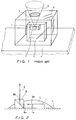
- FIG. 2 illustrates a semiconductor light-emitting device according to a prefered embodiment of the present invention.
- the semiconductor light-emitting device comprises a semiconductor light-emitting element 1 fixedly mounted on a base 4 and emitting light 6 from its light-emitting region 1a, and a beam splitter 8 also fixed to the base 4.
- a transparent resin 5 covers the entirety of the light-emitting element 1 on the base 4, and also a substantial portion of the beam splitter 8, including a light incident portion of a surface 8a thereof, while leaving a light exit surface 8b exposed, whereby the entirety of the optical path 6a for light from the semiconductor light-emitting element 1 extending between the element 1 and the beam splitter 8 is located in the resin 5.
- the resin 5 is transparent to light emitted by the semiconductor light-emitting element 1.
- a cyclic aliphatic epoxy resin for example, may be used.
- Another resin such as diglycidyl ester, may also be usable.
- the transparent resin 5 adheres to and fills the space between the light-emitting region 1a of the light-emitting element 1 and the light incident surface 8a of the beam splitter 8, leaving no gap between the resin 5 and the region 1a or between the resin and the light entrance portion of the surface 8a.
- the light 6 emitted by the semiconductor light-emitting element 1 passes through the transparent resin 5, enters into the beam splitter 8 where it is deflected 90°, and emerges from the device from the surface 8b of the beam splitter 8. Since the beam splitter 8 has its light-incident surface 8a well-finished so as to give no distortion to light intensity distribution and, furthermore, it is in intimately contact with the resin, the light 6 emitted from the semiconductor light-emitting element 1 can emerge from the device without being distorted.
- optical elements for example, glass plates, other than the ones used in the described embodiment may be used.
- the optical elements usable in the present invention are light transmissive. Types, numbers and arrangements of optical elements in the sealing resin are determined in accordance with the purpose of the light-emitting device.
- the surface of sealing resin need not be provided with any special finishing as is provided for optical elements in order to produce undistorted, stable light output from a semiconductor light-emitting device because light emerges from the device through a well-finished surface of an optical element. Furthermore, because the light-emitting element is sealed in a resin, its stability against environment is improved, and also, the positional relationship between the light-emitting element and the associated optical element(s) can be maintained fixed.
Description
- This invention relates to a semiconductor light-emitting device which can be used in a light pickup of an optical disc apparatus, or as a module in an optical communications system, or the like, as ontlined in the preamble of
claim 1. - Generally, a conventional semiconductor light-emitting device comprises a semiconductor light-emitting element mounted on a heat sink block which, in turn, is mounted on a stem. The semiconductor light-emitting element, the heat sink block and the stem are covered by a hollow envelope joined to the stem. Light goes out through a glass window provided in the hollow envelope. With this structure, the light-emitting element can be operated in a hermetically sealed, stable environment.
- In view of stability against environment, easy production, and reduced manufacturing cost of such semiconductor light-emitting devices, resin-molding is considered to be more advantageous. For example, as shown in Figure 1, a semiconductor light-
emitting element 1 is mounted on abase 4 with anSi submount 2 and aheat sink block 3 interposed therebetween, and theelement 1, thesubmount 2 and theheat sink block 3 are sealed in a transparent resin on thebase 4. Light 6 emitted from the semiconductor light-emittingelement 1 emerges through thetransparent resin 5. - The emitted
light 6 from the semiconductor light-emittingelement 1 of the semiconductor light-emitting device shown in Figure 1 is usually made to pass through one or more of optical elements, such as a beam splitter, a lens, an optical fiber, a glass plate and the like. The emittedlight 6 must have an optically undistorted light intensity distribution so that coupling of light to an optical system is not adversely affected. If the light intensity distribution is distorted, it is difficult to obtain for example, a parallel light beam. The emittedlight 6 emerges from the device through asurface portion 7 of the transparent resin, and, therefore, the flatness of thesurface portion 7 which interfaces with exterior is critical. If theportion 7 does not have an optically desirable surface state, the light intensity distribution of the emittedlight 6 is distorted and, therefore, undesired optical coupling with a succeeding optical system may result. In order to provide an optically desirable surface for theportion 7, theportion 7 could be finished by, for example, polishing. However, it is difficult to provide such working as to give flatness of the same degree as those of optical elements to thesurface portion 7, and the productivity of such finishing is low. Furthermore, since ordinary resins are easily damaged and poor in etch-resistance, a surface of such resins is not suitable for use as a light emerging surface. - From Electronic Design Vol. 30, No. 10, May 1982, pages 35 - 36, and Wireless World, No. 1581, June 1984, pages 27-30, as well as from GB-A-2046472, it is known to couple an optical fiber to a semiconducter light-emitting device by enclosing one end of said fiber and the said light-emitting device by a transparent resin.
- According to the present invention, a semiconductor light-emitting device as outlined in
claim 1 is provided. - A semiconductor light-emitting device according to the present invention includes a semiconductor light-emitting element and a beam splitter or a glass plate disposed in such a predetermined position that light emitted by the semiconductor light-emitting element travels through said elements. The light-emitting element and part of said optical element are sealed in a transparent resin member comprising a resin which is transparent to the light emitted by the semiconductor light-emitting element, in such a manner that the entire optical path extruding between the semiconductor light-emitting element and the light entrance portion of said optical element is positioned within the resin member. The light exit portion of said optical element from which the light emitted by the semiconductor light-emitting element exits the device is positioned outside of the resin member.
- According to additional feature of the present invention, at least one additional optical element can be disposed in the optical path between the semiconductor light-emitting element and the light entrance portion of the cited optical element.
- Since the optical path extending between the semiconductor light-emitting element and the optical element is within the resin, output light from the semiconductor light-emitting device does not pass through an interface between the resin and the outer space surrounding the resin, the intensity distribution of the emitted light is not disturbed and, therefore, undistorted light output can be provided from the exit portion of the optical element positioned outside the resin member. The resin member isolates the semiconductor light-emitting element from the external atmosphere and also secures the light-emitting element and the optical element in a predetermined positional relationship.
- Figure 1 is a perspective view schematically illustrating the structure of a conventional semiconductor light-emitting device as explained in detail above;
- Figure 2 is a cross-sectional side view schematically illustrating the structure of a semiconductor light-emitting device according to an embodiment of the present invention;
- Figure 2 illustrates a semiconductor light-emitting device according to a prefered embodiment of the present invention. The semiconductor light-emitting device comprises a semiconductor light-emitting
element 1 fixedly mounted on abase 4 and emittinglight 6 from its light-emitting region 1a, and abeam splitter 8 also fixed to thebase 4. Atransparent resin 5 covers the entirety of the light-emittingelement 1 on thebase 4, and also a substantial portion of thebeam splitter 8, including a light incident portion of asurface 8a thereof, while leaving alight exit surface 8b exposed, whereby the entirety of theoptical path 6a for light from the semiconductor light-emittingelement 1 extending between theelement 1 and thebeam splitter 8 is located in theresin 5. Theresin 5 is transparent to light emitted by the semiconductor light-emittingelement 1. A cyclic aliphatic epoxy resin, for example, may be used. Another resin, such as diglycidyl ester, may also be usable. Thetransparent resin 5 adheres to and fills the space between the light-emitting region 1a of the light-emittingelement 1 and thelight incident surface 8a of thebeam splitter 8, leaving no gap between theresin 5 and the region 1a or between the resin and the light entrance portion of thesurface 8a. - The
light 6 emitted by the semiconductor light-emittingelement 1 passes through thetransparent resin 5, enters into thebeam splitter 8 where it is deflected 90°, and emerges from the device from thesurface 8b of thebeam splitter 8. Since thebeam splitter 8 has its light-incident surface 8a well-finished so as to give no distortion to light intensity distribution and, furthermore, it is in intimately contact with the resin, thelight 6 emitted from the semiconductor light-emittingelement 1 can emerge from the device without being distorted. - Optical elements, for example, glass plates, other than the ones used in the described embodiment may be used. The optical elements usable in the present invention are light transmissive. Types, numbers and arrangements of optical elements in the sealing resin are determined in accordance with the purpose of the light-emitting device.
- With the above-described arrangement of the present invention, the surface of sealing resin need not be provided with any special finishing as is provided for optical elements in order to produce undistorted, stable light output from a semiconductor light-emitting device because light emerges from the device through a well-finished surface of an optical element. Furthermore, because the light-emitting element is sealed in a resin, its stability against environment is improved, and also, the positional relationship between the light-emitting element and the associated optical element(s) can be maintained fixed.
Claims (4)
- A semiconductor light-emitting device comprising:
a semiconductor light-emitting element (1);
an optical element (8) disposed in a predetermined positional relationship with said light-emitting element (1) such that light (6) emitted from said light-emitting element (1) travels through said optical element (8) and
a resin (5) sealing and holding said semiconductor light-emitting element (1) and said optical element (8) in said predetermined positional relationship, said resin being transparent to light (6) emitted from said light-emitting element (1),
characterized in that said optical element (8) is a beam splitter or glass plate, the beam entrance surface (8a) of said optical element (8) being in contact with said resin (5), the beam exit surface (8b) of said optical element (8) being not covered by said resin, and the entire optical path for light emitted from said light-emitting element extending from said light-emitting element to the beam enhance surface (8a) of said optical element is located within said resin (5). - A semiconductor light-emitting device according to claim 1,
characterized in that at least one additional optical element is disposed between the beam exit surface (1a) of said semiconductor light-emitting element (1) and the beam entrance surface (8a) of said optical element (8). - A semiconductor light-emitting device according to claim 1 or 2,
characterized in that said resin (5) is a cyclic aliphatic epoxy resin. - A semiconductor light-emitting device according to claim 1 or 2,
characterized in that said resin (5) is diglycidyl ester.
Applications Claiming Priority (2)
| Application Number | Priority Date | Filing Date | Title |
|---|---|---|---|
| JP189917/90 | 1990-07-16 | ||
| JP2189917A JP2792722B2 (en) | 1990-07-16 | 1990-07-16 | Semiconductor light emitting device |
Publications (2)
| Publication Number | Publication Date |
|---|---|
| EP0466975A1 EP0466975A1 (en) | 1992-01-22 |
| EP0466975B1 true EP0466975B1 (en) | 1993-05-05 |
Family
ID=16249375
Family Applications (1)
| Application Number | Title | Priority Date | Filing Date |
|---|---|---|---|
| EP90124199A Expired - Lifetime EP0466975B1 (en) | 1990-07-16 | 1990-12-14 | Semiconductor light-emitting device |
Country Status (5)
| Country | Link |
|---|---|
| US (1) | US5105237A (en) |
| EP (1) | EP0466975B1 (en) |
| JP (1) | JP2792722B2 (en) |
| KR (1) | KR950000112B1 (en) |
| DE (1) | DE69001548T2 (en) |
Families Citing this family (18)
| Publication number | Priority date | Publication date | Assignee | Title |
|---|---|---|---|---|
| US5444726A (en) * | 1990-11-07 | 1995-08-22 | Fuji Electric Co., Ltd. | Semiconductor laser device |
| US5590144A (en) * | 1990-11-07 | 1996-12-31 | Fuji Electric Co., Ltd. | Semiconductor laser device |
| TW253996B (en) * | 1992-04-07 | 1995-08-11 | Fuji Electric Co Ltd | |
| US5367530A (en) * | 1992-05-29 | 1994-11-22 | Sanyo Electric Co., Ltd. | Semiconductor laser apparatus |
| JP2565279B2 (en) * | 1992-09-25 | 1996-12-18 | 日本電気株式会社 | Optical coupling structure |
| US5414293A (en) * | 1992-10-14 | 1995-05-09 | International Business Machines Corporation | Encapsulated light emitting diodes |
| DE69218431T2 (en) * | 1992-10-14 | 1997-09-25 | Ibm | Encapsulated, light emitting diode and encapsulation process |
| US5516727A (en) * | 1993-04-19 | 1996-05-14 | International Business Machines Corporation | Method for encapsulating light emitting diodes |
| JPH09307144A (en) * | 1996-05-14 | 1997-11-28 | Matsushita Electric Ind Co Ltd | Light emitting element and its manufacture |
| DE19714170C1 (en) * | 1997-03-21 | 1998-07-30 | Siemens Ag | Electro-optical coupler with circuitry and converters, separated from optical fibres by filled coupling gap |
| JP2001021775A (en) | 1999-07-09 | 2001-01-26 | Sumitomo Electric Ind Ltd | Optical device |
| US6999237B2 (en) * | 2001-09-12 | 2006-02-14 | Lightmaster Systems, Inc. | Method and apparatus for configuration and assembly of a video projection light management system |
| US20030151832A1 (en) * | 2002-01-14 | 2003-08-14 | Arthur Berman | Method and apparatus for enclosing optical assemblies |
| WO2003027743A1 (en) * | 2001-09-14 | 2003-04-03 | Infineon Technologies Ag | Transmitter and/or receiver arrangement for optical signal transmission |
| US8076782B2 (en) | 2002-04-01 | 2011-12-13 | Ibiden Co., Ltd. | Substrate for mounting IC chip |
| JPWO2005052666A1 (en) * | 2003-11-27 | 2008-03-06 | イビデン株式会社 | IC chip mounting substrate, motherboard substrate, optical communication device, IC chip mounting substrate manufacturing method, and motherboard substrate manufacturing method |
| JP2008032522A (en) * | 2006-07-28 | 2008-02-14 | Nitta Ind Corp | Tactile sensor using optical fiber |
| WO2016164035A1 (en) | 2015-04-10 | 2016-10-13 | Hewlett Packard Enterprise Development Lp | Overmolded filters |
Family Cites Families (14)
| Publication number | Priority date | Publication date | Assignee | Title |
|---|---|---|---|---|
| DE226431C (en) * | ||||
| JPS5333436A (en) * | 1976-09-09 | 1978-03-29 | Toshiba Corp | Alloy for high frequency induction heating vessel |
| US4478588A (en) * | 1978-03-06 | 1984-10-23 | Amp Incorporated | Light emitting diode assembly |
| JPS54127691A (en) * | 1978-03-28 | 1979-10-03 | Toshiba Corp | Semiconductor light emission device |
| JPS5545236U (en) * | 1978-09-16 | 1980-03-25 | ||
| DE2913262C2 (en) * | 1979-04-03 | 1982-04-29 | Kabelwerke Reinshagen Gmbh, 5600 Wuppertal | Electro-optical connector |
| JPS566038U (en) * | 1979-06-25 | 1981-01-20 | ||
| DE3016103A1 (en) * | 1980-04-25 | 1981-10-29 | Siemens AG, 1000 Berlin und 8000 München | METHOD FOR PRODUCING TRANSPARENT GOAT RESINS |
| JPS5850572A (en) * | 1981-09-22 | 1983-03-25 | 株式会社東芝 | Manufacture of display |
| EP0114258A1 (en) * | 1982-11-30 | 1984-08-01 | Kabushiki Kaisha Toshiba | Resin encapsulation type photo-semiconductor devices |
| JPH084155B2 (en) * | 1986-06-25 | 1996-01-17 | 松下電器産業株式会社 | Optical connector module |
| JPS6314489A (en) * | 1986-07-04 | 1988-01-21 | Mitsubishi Electric Corp | Semiconductor laser device |
| JPS6333877A (en) * | 1986-07-29 | 1988-02-13 | Omron Tateisi Electronics Co | Photo-semiconductor device |
| JP2504533B2 (en) * | 1988-09-02 | 1996-06-05 | 同和鉱業株式会社 | LED light emitting device and method of manufacturing light emitting block used in the device |
-
1990
- 1990-07-16 JP JP2189917A patent/JP2792722B2/en not_active Expired - Lifetime
- 1990-12-14 EP EP90124199A patent/EP0466975B1/en not_active Expired - Lifetime
- 1990-12-14 DE DE9090124199T patent/DE69001548T2/en not_active Expired - Lifetime
-
1991
- 1991-07-03 US US07/724,460 patent/US5105237A/en not_active Expired - Lifetime
- 1991-07-15 KR KR1019910012007A patent/KR950000112B1/en not_active IP Right Cessation
Also Published As
| Publication number | Publication date |
|---|---|
| JP2792722B2 (en) | 1998-09-03 |
| JPH0474483A (en) | 1992-03-09 |
| KR950000112B1 (en) | 1995-01-09 |
| DE69001548T2 (en) | 1993-09-09 |
| DE69001548D1 (en) | 1993-06-09 |
| KR920003566A (en) | 1992-02-29 |
| US5105237A (en) | 1992-04-14 |
| EP0466975A1 (en) | 1992-01-22 |
Similar Documents
| Publication | Publication Date | Title |
|---|---|---|
| EP0466975B1 (en) | Semiconductor light-emitting device | |
| US4355323A (en) | Coupler comprising a light source and lens | |
| US4733094A (en) | Bidirectional optoelectronic component operating as an optical coupling device | |
| US5566265A (en) | Transmission and reception module for a bidirectional, optical message and signal transmission | |
| US8827572B2 (en) | Side coupling optical fiber assembly and fabrication method thereof | |
| EP0611975B1 (en) | Subassembly for optoelectronic devices | |
| US6731882B1 (en) | Leadframe-based optoelectronic bidirectional transmitting and receiving module | |
| US6932519B2 (en) | Optical device package | |
| US6588949B1 (en) | Method and apparatus for hermetically sealing photonic devices | |
| US20050180698A1 (en) | Light transmitting modules with optical power monitoring | |
| US6786627B2 (en) | Light generating module | |
| JPH10321900A (en) | Optical module | |
| US5255333A (en) | Opto-electronic transducer arrangement having a lens-type optical coupling | |
| JPH05175552A (en) | Mounting structure of optical element board | |
| US20040017978A1 (en) | Optical module | |
| JPH06151903A (en) | Photo-electric transfer element and optical fiber coupling module | |
| KR100527160B1 (en) | the package structure for bi-directional optical modules | |
| JPH10307237A (en) | Integrated type semiconductor device for optical communication | |
| US20040258367A1 (en) | Electrooptical module | |
| JPH06342114A (en) | Airtight optical connector | |
| JP3295327B2 (en) | Bidirectional optical module | |
| US6808321B2 (en) | Optical communication module | |
| JPS5925284A (en) | Photosemiconductor device | |
| JPH0521899A (en) | Semiconductor laser device | |
| JPH10268162A (en) | Light module |
Legal Events
| Date | Code | Title | Description |
|---|---|---|---|
| PUAI | Public reference made under article 153(3) epc to a published international application that has entered the european phase |
Free format text: ORIGINAL CODE: 0009012 |
|
| 17P | Request for examination filed |
Effective date: 19901214 |
|
| AK | Designated contracting states |
Kind code of ref document: A1 Designated state(s): DE FR NL |
|
| 17Q | First examination report despatched |
Effective date: 19920311 |
|
| GRAA | (expected) grant |
Free format text: ORIGINAL CODE: 0009210 |
|
| AK | Designated contracting states |
Kind code of ref document: B1 Designated state(s): DE FR NL |
|
| REF | Corresponds to: |
Ref document number: 69001548 Country of ref document: DE Date of ref document: 19930609 |
|
| ET | Fr: translation filed | ||
| PLBE | No opposition filed within time limit |
Free format text: ORIGINAL CODE: 0009261 |
|
| STAA | Information on the status of an ep patent application or granted ep patent |
Free format text: STATUS: NO OPPOSITION FILED WITHIN TIME LIMIT |
|
| 26N | No opposition filed | ||
| REG | Reference to a national code |
Ref country code: FR Ref legal event code: D6 |
|
| PGFP | Annual fee paid to national office [announced via postgrant information from national office to epo] |
Ref country code: NL Payment date: 20091216 Year of fee payment: 20 |
|
| PGFP | Annual fee paid to national office [announced via postgrant information from national office to epo] |
Ref country code: FR Payment date: 20091221 Year of fee payment: 20 |
|
| PGFP | Annual fee paid to national office [announced via postgrant information from national office to epo] |
Ref country code: DE Payment date: 20091222 Year of fee payment: 20 |
|
| REG | Reference to a national code |
Ref country code: NL Ref legal event code: V4 Effective date: 20101214 |
|
| PG25 | Lapsed in a contracting state [announced via postgrant information from national office to epo] |
Ref country code: NL Free format text: LAPSE BECAUSE OF EXPIRATION OF PROTECTION Effective date: 20101214 |
|
| PG25 | Lapsed in a contracting state [announced via postgrant information from national office to epo] |
Ref country code: DE Free format text: LAPSE BECAUSE OF EXPIRATION OF PROTECTION Effective date: 20101214 |