EP0466950B1 - Method for producing an epoxy resin composition for use in molding photosemiconductor - Google Patents
Method for producing an epoxy resin composition for use in molding photosemiconductor Download PDFInfo
- Publication number
- EP0466950B1 EP0466950B1 EP90113625A EP90113625A EP0466950B1 EP 0466950 B1 EP0466950 B1 EP 0466950B1 EP 90113625 A EP90113625 A EP 90113625A EP 90113625 A EP90113625 A EP 90113625A EP 0466950 B1 EP0466950 B1 EP 0466950B1
- Authority
- EP
- European Patent Office
- Prior art keywords
- epoxy resin
- resin composition
- molding
- photosemiconductor
- organic solvent
- Prior art date
- Legal status (The legal status is an assumption and is not a legal conclusion. Google has not performed a legal analysis and makes no representation as to the accuracy of the status listed.)
- Expired - Lifetime
Links
Images




Classifications
-
- H—ELECTRICITY
- H10—SEMICONDUCTOR DEVICES; ELECTRIC SOLID-STATE DEVICES NOT OTHERWISE PROVIDED FOR
- H10F—INORGANIC SEMICONDUCTOR DEVICES SENSITIVE TO INFRARED RADIATION, LIGHT, ELECTROMAGNETIC RADIATION OF SHORTER WAVELENGTH OR CORPUSCULAR RADIATION
- H10F77/00—Constructional details of devices covered by this subclass
- H10F77/50—Encapsulations or containers
-
- C—CHEMISTRY; METALLURGY
- C08—ORGANIC MACROMOLECULAR COMPOUNDS; THEIR PREPARATION OR CHEMICAL WORKING-UP; COMPOSITIONS BASED THEREON
- C08G—MACROMOLECULAR COMPOUNDS OBTAINED OTHERWISE THAN BY REACTIONS ONLY INVOLVING UNSATURATED CARBON-TO-CARBON BONDS
- C08G59/00—Polycondensates containing more than one epoxy group per molecule; Macromolecules obtained by polymerising compounds containing more than one epoxy group per molecule using curing agents or catalysts which react with the epoxy groups
- C08G59/18—Macromolecules obtained by polymerising compounds containing more than one epoxy group per molecule using curing agents or catalysts which react with the epoxy groups ; e.g. general methods of curing
- C08G59/20—Macromolecules obtained by polymerising compounds containing more than one epoxy group per molecule using curing agents or catalysts which react with the epoxy groups ; e.g. general methods of curing characterised by the epoxy compounds used
- C08G59/22—Di-epoxy compounds
- C08G59/24—Di-epoxy compounds carbocyclic
- C08G59/245—Di-epoxy compounds carbocyclic aromatic
-
- C—CHEMISTRY; METALLURGY
- C08—ORGANIC MACROMOLECULAR COMPOUNDS; THEIR PREPARATION OR CHEMICAL WORKING-UP; COMPOSITIONS BASED THEREON
- C08G—MACROMOLECULAR COMPOUNDS OBTAINED OTHERWISE THAN BY REACTIONS ONLY INVOLVING UNSATURATED CARBON-TO-CARBON BONDS
- C08G59/00—Polycondensates containing more than one epoxy group per molecule; Macromolecules obtained by polymerising compounds containing more than one epoxy group per molecule using curing agents or catalysts which react with the epoxy groups
- C08G59/18—Macromolecules obtained by polymerising compounds containing more than one epoxy group per molecule using curing agents or catalysts which react with the epoxy groups ; e.g. general methods of curing
- C08G59/40—Macromolecules obtained by polymerising compounds containing more than one epoxy group per molecule using curing agents or catalysts which react with the epoxy groups ; e.g. general methods of curing characterised by the curing agents used
- C08G59/42—Polycarboxylic acids; Anhydrides, halides or low molecular weight esters thereof
- C08G59/4215—Polycarboxylic acids; Anhydrides, halides or low molecular weight esters thereof cycloaliphatic
-
- C—CHEMISTRY; METALLURGY
- C08—ORGANIC MACROMOLECULAR COMPOUNDS; THEIR PREPARATION OR CHEMICAL WORKING-UP; COMPOSITIONS BASED THEREON
- C08L—COMPOSITIONS OF MACROMOLECULAR COMPOUNDS
- C08L63/00—Compositions of epoxy resins; Compositions of derivatives of epoxy resins
-
- H—ELECTRICITY
- H10—SEMICONDUCTOR DEVICES; ELECTRIC SOLID-STATE DEVICES NOT OTHERWISE PROVIDED FOR
- H10F—INORGANIC SEMICONDUCTOR DEVICES SENSITIVE TO INFRARED RADIATION, LIGHT, ELECTROMAGNETIC RADIATION OF SHORTER WAVELENGTH OR CORPUSCULAR RADIATION
- H10F77/00—Constructional details of devices covered by this subclass
- H10F77/40—Optical elements or arrangements
- H10F77/413—Optical elements or arrangements directly associated or integrated with the devices, e.g. back reflectors
-
- H—ELECTRICITY
- H10—SEMICONDUCTOR DEVICES; ELECTRIC SOLID-STATE DEVICES NOT OTHERWISE PROVIDED FOR
- H10W—GENERIC PACKAGES, INTERCONNECTIONS, CONNECTORS OR OTHER CONSTRUCTIONAL DETAILS OF DEVICES COVERED BY CLASS H10
- H10W72/00—Interconnections or connectors in packages
- H10W72/851—Dispositions of multiple connectors or interconnections
- H10W72/874—On different surfaces
- H10W72/884—Die-attach connectors and bond wires
-
- H—ELECTRICITY
- H10—SEMICONDUCTOR DEVICES; ELECTRIC SOLID-STATE DEVICES NOT OTHERWISE PROVIDED FOR
- H10W—GENERIC PACKAGES, INTERCONNECTIONS, CONNECTORS OR OTHER CONSTRUCTIONAL DETAILS OF DEVICES COVERED BY CLASS H10
- H10W74/00—Encapsulations, e.g. protective coatings
-
- H—ELECTRICITY
- H10—SEMICONDUCTOR DEVICES; ELECTRIC SOLID-STATE DEVICES NOT OTHERWISE PROVIDED FOR
- H10W—GENERIC PACKAGES, INTERCONNECTIONS, CONNECTORS OR OTHER CONSTRUCTIONAL DETAILS OF DEVICES COVERED BY CLASS H10
- H10W90/00—Package configurations
- H10W90/701—Package configurations characterised by the relative positions of pads or connectors relative to package parts
- H10W90/731—Package configurations characterised by the relative positions of pads or connectors relative to package parts of die-attach connectors
- H10W90/736—Package configurations characterised by the relative positions of pads or connectors relative to package parts of die-attach connectors between a chip and a stacked lead frame, conducting package substrate or heat sink
-
- H—ELECTRICITY
- H10—SEMICONDUCTOR DEVICES; ELECTRIC SOLID-STATE DEVICES NOT OTHERWISE PROVIDED FOR
- H10W—GENERIC PACKAGES, INTERCONNECTIONS, CONNECTORS OR OTHER CONSTRUCTIONAL DETAILS OF DEVICES COVERED BY CLASS H10
- H10W90/00—Package configurations
- H10W90/701—Package configurations characterised by the relative positions of pads or connectors relative to package parts
- H10W90/751—Package configurations characterised by the relative positions of pads or connectors relative to package parts of bond wires
- H10W90/756—Package configurations characterised by the relative positions of pads or connectors relative to package parts of bond wires between a chip and a stacked lead frame, conducting package substrate or heat sink
Definitions
- the present invention relates to a method for molding a photosemiconductor for a photosemiconductor device free of optical unevenness, said photosemiconductor comprising an epoxy resin composition.
- JP-A-60-137046 discloses an epoxy resin composition obtained by mixing an acid anhydride curing agent, a liquid epoxy resin and a metal salt of carboxylic acid/imidazole curing catalyst.
- US-A-4732962 discloses a composition comprising a bisphenol-A type epoxy resin, an anhydride curing agent, an imidazole catalyst and optionally a filler system.
- DE-A-3012523 discloses the use of epoxy/anhydride compositions for encapsulating radiation sensitive semiconductor devices.
- GB-A-1350156 discloses a process for producing modified internally plasticized epoxy resins.
- Fig. 3 illustrates, an epoxy resin composition in tablet form for photosemiconductor molding is fed to a cull 1 and pressed by a plunger 2, upon which the epoxy resin composition flows, as the arrows show, through a runner 3 into a cavity 4.
- Fig. 3 illustrates, an epoxy resin composition in tablet form for photosemiconductor molding is fed to a cull 1 and pressed by a plunger 2, upon which the epoxy resin composition flows, as the arrows show, through a runner 3 into a cavity 4.
- the epoxy resin composition for photosemiconductor molding passes through a gate 5 and flows into the cavity 4, where a solid state image forming element 7 mounted on a frame 6 in the cavity 4 is molded with the epoxy resin composition, as the arrows show.
- an area sensor of the solid state image forming element 7 is molded with a conventional epoxy resin composition for photosemiconductor molding by the method described above and intense parallel light rays are allowed to strike upon the molded area sensor with an iris diaphragm of F-32, such optical unevenness in the molding resin as that described above causes the resulting image to have a striped pattern.
- the present inventors conducted a series of extensive studies in order to eliminate optical unevenness from the cured resins obtained from epoxy resin compositions for use in photosemiconductor molding. As a result, it was found that the formation of optical unevenness is greatly affected by the refractive index distribution of the cured resin. Further studies have been made with regard to refractive index distribution and, as a result, it has now been found that a cured resin with no optical unevenness can be obtained by making the refractive index distribution curve of the cured resin sharp so as to satisfy the specific requirements (A), (B), and (C) described later. The present invention has been completed based on the above finding.
- an object of the present invention is to provide a method for molding photosemiconductors for a photosemiconductor device free from optical unevenness.
- the present invention relates to a method for molding photosemiconductors comprising producing an epoxy resin composition comprising the steps of:
- the epoxy resin composition obtained by the process for molding photosemiconductors according to the present invention can be used for a photosemiconductor device comprising said photosemiconductor element molded with said cured transparent epoxy resin composition.
- the cured transparent epoxy resin composition obtained by the method according to the present invention has a refractive index distribution curve characterised by the following (A), (B), and (C):
- a photosemiconductor element is molded in a cured transparent epoxy resin composition which satisfies the above requirements (A), (B) and (C).
- the cured resin satisfying the requirements (A), (B), and (C) has a narrower refractive index distribution, i.e., a sharper refractive index distribution curve, than the cured resins obtained from conventional epoxy resin compositions.
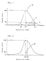
- Fig. 1 is a bell-shaped refractive index distribution curve of one example of the cured transparent epoxy resin composition employed in the present invention
- K indicates the refractive index distribution curve
- (a) indicates the refractive index value corresponding to the maximum peak of the distribution curve
- (b) and (c) indicate refractive index values respectively correspond to those points on the refractive index distribution curve which have a relative height of 20 with the height of the maximum peak being taken as 100 and which respectively are on the left and right of the maximum peak
- X is the refractive index difference between the refractive index values (b) and (c)
- Y is the refractive index difference which is the larger one of the difference between the refractive index value (a) corresponding to the maximum peak and the refractive index value (b) and the difference between the refractive index values (a) and (c) (in the figure, Y is the difference between (a) and (c) because this difference is larger than the
- the cured resin can be made applicable to future solid state image forming elements which may possibly have greatly increased picture element numbers, without causing problems ascribable to optical unevenness, by regulating the refractive index difference Z, which is the largest one of the differences between the refractive index value (a) corresponding to the maximum peak and refractive index value(s) corresponding to the other peak(s) (in Fig. 2, Z is the refractive index difference between (a) and (a')), at 0.0010 or less, preferably at 0.0003 or less.
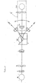
- the refractive index curves shown in Figs. 1 and 2 referred to above can be obtained by measurement with a refractive index-measuring apparatus utilizing the principle shown in Fig. 6.
- F indicates an interference filter
- SL a spectral illuminant lamp
- S 1 an inlet slit
- S 2 an outlet slit
- L 1 a collimator lens
- L 2 a telemeter lens
- P V-block prism
- SM sample to be tested
- P.M a photomultiplier
- N a telemeter part.
- a cured transparent epoxy resin composition is formed, for example, into a cubic sample SM, two adjacent sides of the cubic sample are polished by buffing so as to have a surface roughness of 1.5 ⁇ m or less, and this sample is set on the V-block prism P having a V-shaped depression with the polished sides of the sample being in contact with the V-shaped depression walls. Then, light is emitted from the illuminant SL. The light emitted from the illuminant SL is converted to monochromatic light by the interference filter F, and the monochromatic light passes through the inlet slit S 1 and then converted to parallel rays of light by the collimator lens L 1 .
- the parallel light rays pass through the V-block prism P, the sample SM, and the V-block prism P in this order, while the parallel light rays are being polarized upward and downward relative to the light axis due to the difference in refractive index between the V-block prism P and the sample SM.
- the telemeter part N equipped with the telemeter lens L 2 , the outlet slit S 2 , and the photomultiplier P.M, oscillates as shown by the arrows by means of a pulse motor (not shown) and receives the polarized light at each position in the oscillation movement, and the amount of the received light is indicated on a display (not shown) as the amount of energy.
- the relationship between refractive index and each angle in the above oscillation movement has been determined beforehand. Therefore, the amount of light received at a given angle means the amount of light refracted at an angle corresponding to that given angle.
- this refractive index-measuring apparatus includes that produced and marketed by Karunew Optics Company, Japan under the trade name of Automatic Refractometer KPR-200.
- the measurement of refractive index in the present invention is made by means of this refractometer with sodium D-line (587.6 nm) being used as the measuring light.
- the cured transparent epoxy resin composition free of optical unevenness is one whose refractive index distribution curve obtained by the method as described above is sharp and satisfies the requirements (A), (B), and (C) described hereinabove.
- An epoxy resin composition which can cure into a resin having such a sharp refractive index distribution curve may be produced, for example, by uniformly dispersing each of the constituent ingredients in the epoxy resin composition.
- Examples of the technique of uniformly dispersing ingredients to produce an epoxy resin composition for use in photosemiconductor molding include: (1) a method in which a conventional powdery epoxy resin composition for molding use which has been made to be in the B-stage (semi-cured state) is mixed sufficiently with an organic solvent to dissolve each component, and then the organic solvent is evaporated; (2) a method in which raw ingredients such as an epoxy resin, a hardener, a curing accelerator, and others are mixed with and uniformly dissolved in an organic solvent, the resulting solution is heated so as to result in a B-stage composition, and then the solvent is evaporated; and (3) a method in which the same solution as that obtained in (2) above is prepared, subsequently the solvent is evaporated, and then the residue is heated mildly to form a B-stage composition.
- the other peak can be weakened by reducing the epoxy resin composition to a uniformly mixed fine powder, thereby giving a bell-shaped distribution curve having the maximum peak a only as shown in Fig. 1.
- the term fine powder herein normally means a powder in which particles having maximum particle diameters of 30 ⁇ m or less, preferably 10 ⁇ m or less, comprise 90 wt% or more of the powder.
- a B-stage (semi-cured) epoxy resin composition is prepared by mixing the above-mentioned ingredient.
- a partial reaction method (semi-curing method) and melt-mixing method are generally used.
- the degree of reaction of the B-stage epoxy resin composition is generally such an extent that the gelation time of the resin composition at 150°C be from 10 to 70 seconds, and preferably from 10 to 40 seconds.
- the B-stage epoxy resin composition is uniformly dissolved in an organic solvent.
- the ingredients of the resin composition are mixed with each other uniformly to the molecular level.
- the organic solvent is then removed by evaporation from the solution, and the residue is cooled to room temperature and pulverized by a conventional method.
- the pulverized resin composition is stamped into tablets if desired.
- the degree of reaction of the thus-obtained final epoxy resin composition is generally such an extent that a transfer molding process can be carried out and that the gelation time at 150°C is from 10 to 50 seconds, and preferably from 10 to 40 seconds.
- the resin composition may be heated after removing the organic solvent, for example in order to adjust the viscosity of the resin composition. At this time, if the resin composition is heated vigorously, unevenness of the curing degree due to unevenness of the reaction rate develops. Therefore, the heating of the resin composition is preferably carried out gradually at a low temperature so that the gelation time at 150°C does not lower than 20 seconds.
- the ingredients are firstly dissolved in an organic solvent.
- the ingredients of the resin composition are mixed with each other uniformly to the molecular level.
- the resulting solution is heated to proceed the curing reaction so as to convert the resin composition to the B-stage.
- the organic solvent is then removed by evaporation from the solution, and the residue is cooled to room temperature and pulverized by a conventional method.
- the pulverized resin composition is stamped into tablets if desired.
- the ingredients may be heated simultaneously with dissolving in the organic solvent but not heated after completion of dissolving.
- the B-stage resin composition may further heated to heighten the curing degree.
- the heating is preferably carried out gradually at a low temperature so that the gelation time at 150°C does not lower than 20 seconds because of the above reasons.
- the degree of reaction of the thus-obtained final product is generally such an extent that the gelation time at 150°C is from 10 to 70 seconds, and preferably from 10 to 40 seconds. At this time, the extent of gelation after starting evaporation of the organic solvent is preferably controlled such that the gelation time at 150°C does not lower than 20 seconds.
- one, or two or more kinds of each ingredients may be used.
- the term "one kind” used herein includes, in the case of epoxy resins for example, bisphenol A type and bisphenol F type which have the same skeleton and are classified into the bisphenol type, and in the case of hardener, phthalic anhydride and tetrahydrophthalic anhydride which have the same skeleton and are classified into the phthalic acid type.
- one kind of the epoxy resin and one kind of hardener are dissolved in an organic solvent.
- the organic solvent is removed by evaporation from the resulting solution, and the residue is subjected to low temperature heating (low temperature aging) so as to convert the residue into B-stage.
- low temperature heating low temperature aging
- the degree of reaction of the thus-obtained final product is generally such an extent that the gelation time at 150°C is from 10 to 70 seconds, and preferably from 10 to 40 seconds. At this time, the extent of gelation after starting evaporation of the organic solvent is preferably controlled such that the gelation time at 150°C does not lower than 20 seconds.
- the epoxy resin composition for photosemiconductor molding to be used for producing the photosemiconductor device according to the present invention is one which is obtained by use of an epoxy resin, a hardener, and a curing accelerator, and contains no inorganic fillers such as silica powder.
- epoxy resin conventionally known epoxy resins may be used without any particular limitation as long as the epoxy used and the resulting cured composition are less apt to undergo discoloration.
- epoxy resins include bisphenol A epoxy resins, bisphenol F epoxy resins, phenol-novolac epoxy resins, alicyclic epoxy resins, heterocycle-containing epoxy resins such as triglycidyl isocyanurate and hydantoin epoxies, hydrogenated bisphenol A epoxy resins, aliphatic epoxy resins, glycidyl ether epoxy resins, and the like. These may be used alone or in combination.
- acid anhydrides are advantageous in that they are less apt to cause discoloration of the resin composition during or after cure.
- acid anhydrides include phthalic anhydride, maleic anhydride, trimellitic anhydride, pyromellitic anhydride, hexahydrophthalic anhydride, tetrahydrophthalic anhydride, methylnadic anhydride, nadic anhydride and glutaric anhydride.
- hardener examples include amine-type hardeners such as m-phenylenediamine, dimethyldiphenylmethane, diaminodiphenyl sulfone, m-xylenediamine, tetraethylenepentamine, diethylamine and propylamine, and further include phenolic resin-type hardeners. Any of these may be employed.
- amine-type hardeners such as m-phenylenediamine, dimethyldiphenylmethane, diaminodiphenyl sulfone, m-xylenediamine, tetraethylenepentamine, diethylamine and propylamine, and further include phenolic resin-type hardeners. Any of these may be employed.
- the combination in which the epoxy resin is at least one of bisphenol A epoxy resin and bisphenol F epoxy resin, and the hardener is at least one of phthalic anhydride and tetrahydrophthalic anhydride is preferred.
- curing accelerator examples include tertiary amines, imidazole and its derivatives, metal salts of carboxylic acids and phosphorus compounds.
- additives such as anti-discoloring agents, modifiers, anti-deteriorating agents and mold-release agents, may be incorporated, if required and necessary, into the epoxy resin composition for photosemiconductor molding according to this invention.
- anti-discoloring agent conventionally known ones may be mentioned, such as phenolic compounds, amine-type compounds, organosulfur compounds and phosphine-type compounds.
- the organic solvent to be used for producing the epoxy resin composition is not particularly limited as long as it is capable of completely dissolving B-stage epoxy resin compositions for photosemiconductor molding.
- the organic solvent include hydrocarbons such as toluene and xylene, halogenated hydrocarbons such as dichloromethane, 1,1,1-trichloroethane and 1,1,2-trichloroethane, ethers such as diethyl ether, dioxane and tetrahydrofuran, ketones such as acetone, methyl ethyl ketone and diethyl ketone and mixed solvents composed of two or more thereof.
- Neither the mixing ratio of the organic solvent to the epoxy resin composition for photosemiconductor molding nor the temperature for mixing is particularly limited, as long as the epoxy resin composition for photosemiconductor molding can be completely dissolved.
- the amount of the organic solvent used is preferably from 1 to 50 times by weight, more preferably from 1 to 10 times by weight, the amount of the B-stage epoxy resin composition for photosemiconductor molding.
- the mixing temperature is preferably kept at 100°C or lower because too high a temperature results in gelation of the epoxy resin composition for photosemiconductor molding.
- Methods for removing the organic solvent in the above processes are not particularly limited. For example, there may be employed a method in which the solvent is removed under reduced pressure at ordinary temperature or with heating according to need, or a method in which the solvent is removed by freeze drying under vacuum. According to the method of the present invention, the amount of the organic solvent remaining unremoved is 3% by weight or less based on the total amount of the epoxy resin composition for photosemiconductor molding. The content of the remaining organic solvent in the epoxy resin composition is preferably 1.5% by weight or less, and particularly preferably 0.05% by weight or less.
- the epoxy resin composition for photosemiconductor molding tends to have a very short pot life and the cured composition tends to have a lowered glass transition temperature and hence an increased linear expansion coefficient, so that the molding resin may have impaired moisture and heat cycle resistance.
- the epoxy resin composition for photosemiconductor molding obtained by the method described above is in such a state that all the components have been mixed with each other uniformly to the molecular level. Therefore, the refractive index distribution curve of the cured composition is sharp, so that the cured composition has no optical unevenness. Furthermore, since all the components are dissolved in an organic solvent during the production process and, hence, can be easily purified e.g. by suction filtration under reduced pressure or by filtration under pressure using for example an ordinary filter paper, gel-like aggregates and foreign substances including fine dust particles present in the resin composition can be easily removed which have so far been difficult to remove.
- the epoxy resin composition for photosemiconductor molding should be optically transparent since it is to be used in the resin molding of photosemiconductors such as photoreceiving elements.
- transparent used herein means that the cured resin obtained from the epoxy resin composition for photosemiconductor molding has a transmittance of generally 90% or higher, preferably 95% or higher, more preferably 98% or higher, as measured at 600 nm with the cured resin thickness being 1 mm.
- the meaning of "ingredients being mixed with each other uniformly to the molecular level” is as follows.
- the resin composition is transfer molded at 150°C for 6 minutes and then hardened at 150°C for 3 hours.
- the hardened resin composition is taken out from the runner portion of the molding die, and formed into a flat plate (thickness: 3.0 mm, width: 5 mm) having a branch perpendicular to the flat plate, the surface of which is polished to have a surface roughness of 1.5 ⁇ m or less.
- the plate of the cured resin composition is equipped on a solid state image forming element (1/2 inch, 380,000 picture elements).
- Intense parallel light rays having a luminous intensity of 10 candelas are allowed to strike the image forming element with an iris diaphragm of F-32.
- the case where no striped pattern is observed is determined as "mixed uniformly to the molecular level".
- Molding of photoreceiving elements or other photosemiconductors with the epoxy resin composition is not particularly limited, and can be carried out by known molding techniques such as, for example, ordinary transfer molding.
- transfer molding a molding resin composition in a powder form is normally used after being tableted at ordinary temperature.
- the photosemiconductor device thus obtained has a structure as shown in Fig. 5, in which an image-pickup solid element 13 as a photoreceiving element is mounted on a bonding pad 11 through an adhesive 12, and a color filter 15 is bonded to the upper side of the photoreceiving element by means of a transparent adhesive 14, with this assembly being resin-molded in an epoxy resin composition 16 for photosemiconductor molding.
- the color filter 15 has been provided in order to obtain color images, and is unnecessary for monochromatic images.
- numeral 17 denotes a glass plate, 18 a bonding wire, and 19 a lead frame.
- this photosemiconductor device has been resin-molded in a photosemiconductor-molding epoxy resin composition in which all the components thereof have been mixed uniformly to the molecular level, the refractive index distribution curve of the molding resin 16 is sharp, so that the molding resin 16 has no optical unevenness. Therefore, images obtained by operating this device are free from striped patterns ascribable to optical unevenness and black spots due to inclusion of foreign particles.
- the freedom of optical unevenness has been ascertained with photosemiconductor devices obtained by regulating the thickness l of the molding resin over the color filter 15 at ordinary values, i.e., 0.5 to 2 mm.
- the photosemiconductor device of the present invention is free of optical unevenness because the refractive index distribution curve of the cured transparent epoxy resin composition is characterized by (A), (B), and (C) described hereinabove. Furthermore, in the case where the cured transparent epoxy resin is obtained from an epoxy resin composition which has undergone a dissolved state in an organic solvent, foreign substances can be removed from the resin composition by filtration, so that the cured resin can be made free of gel-like aggregates and foreign substances, such as fine dust particles, present in the resin composition, although these impurities have so far been difficult to remove. Thus, the resin composition can be of high quality.
- such a high-quality epoxy resin composition is used for resin-molding of a photoreceiving element, such as a solid state image forming element, to produce a photosemiconductor device according to the present invention
- the images formed by the photosemiconductor device are free from striped patterns ascribable to optical unevenness of molding resin or black spots ascribable to foreign substances present in molding resin. That is, the photosemiconductor device of the present invention, although being of a resin-molded type, has high performance that is equal to or higher than those of ceramic-packaged types.
- epoxy resin compositions A to G were prepared beforehand by the methods given below in which the six formulations shown in Table 1 were used. In Table 1, the formulations are indicated in terms of part by weight.
- Epoxy resin Hardener Formulation Epikote 1001 Triglycidyl isocyanurate tetrahydrophthalic anhydride Catalyst 1 75 25 52.0 0.3 2 75 25 51.9 0.3 3 75 25 51.8 0.3 4 75 25 51.7 0.3 5 75 25 51.4 0.3 6 75 25 51.0 0.3
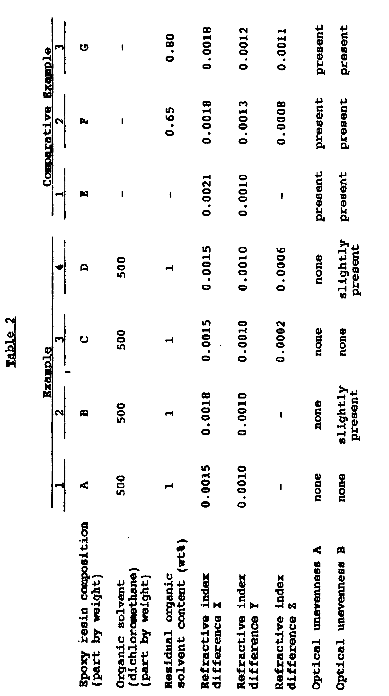
- compositions were prepared according to formulations 1 and 3, respectively, as shown in Table 1. Each of the two compositions was allowed to undergo curing reactions of the epoxy resins thereby to prepare, from each composition, a B-stage epoxy resin composition for photosemiconductor molding which composition had a gelation time as measured at 150°C of 30 seconds. 50 Parts each of the thus-prepared two kinds of B-stage epoxy resin compositions for photosemiconductor molding were blended with each other, and the blend was mixed with and completely dissolved in the organic solvent whose kind and amount are shown in Table 2. The solvent was then removed under reduced pressure, while the solution was being heated at 45°C. The resulting residue was reduced to powder to obtain photosemiconductor-molding epoxy resin composition B in a powder form (for Example 2) having the residual organic solvent content as shown in Table 2 and a gelation time as measured at 150°C of 25 seconds.
- Each of the seven kinds of powdery epoxy resin compositions (A to G) obtained by the methods described above was formed into tablets.
- Each tableted composition was subjected to transfer molding at 150°C for 6 minutes to form a cube, which was then cured at 150°C for 3 hours.
- seven cured cubes each measuring 1 x 1 x 1 cm were prepared from the seven kinds of compositions.
- adjacent two sides were polished by buffing so that the polished surfaces had surface roughnesses of 1.5 ⁇ m or less.
- the thus-obtained cubic samples (A to G) were examined for refractive index distribution by means of a refractometer (Automatic Refractometer KPR-200 manufactured by Karunew Optics Company).
- comparative samples E and F do not satisfy requirement (A) or (B) described hereinabove as apparent from the refractive index distribution curves shown in Figs. 11 and 12 and from the values of X and Y shown in Table 2.
- the other comparative sample G satisfies requirements (A) and (B) as seen from the refractive index distribution curve shown in Fig. 13 and from the values of X and Y in Table 2, but the refractive index difference Z between the refractive index value (a) corresponding to the maximum peak and the refractive index value (a') corresponding to the other peak is above 0.0010. That is, sample G does not satisfy requirement (C) described hereinabove.
- a photosemiconductor device was prepared by actually subjecting an area sensor, which is an image-pickup solid element, to direct molding at 150°C for 6 minutes, followed by postcure at 150°C for 3 hours.
- an area sensor which is an image-pickup solid element
- a camera was constructed.
- intense parallel rays of light (luminous intensity: 10 candelas) were allowed to strike at a right angle, and images took at an iris of F-32 were projected on a display.
- the four kinds of cameras constructed in Examples respectively using compositions A to D gave images free from optical unevenness as shown in Table 2 (Optical unevenness A).
- Optical unevenness A By contrast, in the case of the three kinds of cameras of Comparative Examples constructed by using compositions E to G, respectively, optical unevenness was observed on the images with part of the images having a striped pattern.
Landscapes
- Chemical & Material Sciences (AREA)
- Health & Medical Sciences (AREA)
- Chemical Kinetics & Catalysis (AREA)
- Medicinal Chemistry (AREA)
- Polymers & Plastics (AREA)
- Organic Chemistry (AREA)
- Epoxy Resins (AREA)
- Compositions Of Macromolecular Compounds (AREA)
Description
| Epoxy resin | Hardener | |||
| Formulation | Epikote 1001 | Triglycidyl isocyanurate | tetrahydrophthalic anhydride | |
| 1 | 75 | 25 | 52.0 | 0.3 |
| 2 | 75 | 25 | 51.9 | 0.3 |
| 3 | 75 | 25 | 51.8 | 0.3 |
| 4 | 75 | 25 | 51.7 | 0.3 |
| 5 | 75 | 25 | 51.4 | 0.3 |
| 6 | 75 | 25 | 51.0 | 0.3 |
Claims (5)
- A method for molding photosemiconductors comprising producing an epoxy resin composition comprising the steps of:(a) dissolving into an organic solvent a B-stage epoxy resin, a hardener, and a curing accelerator as constituent ingredients, and then removing the organic solvent to such a degree that the amount of the solvent remaining unremoved becomes 3% by weight or less based on the total amount of the epxoy resin composition, or(b) dissolving an epoxy resin, a hardener, and a curing accelerator into an organic solvent, and then heating the solution to allow the curing reaction of the epoxy resin to proceed to produce a B-stage epoxy resin composition and then removing the organic solvent to such a degree that the amount of the solvent remaining unremoved becomes 3% by weight or less based on the total amount of the epoxy resin composition, or(c) mixing one kind of epoxy resin and one kind of hardener with an organic solvent, removing the organic solvent to such a degree that the amount of the solvent remaining unremoved becomes 3% by weight or less, based on the total amount of the epoxy resin composition, and then allowing the residual epoxy resin composition to undergo the curing reaction of the epoxy resin to produce a B-stage epoxy resin composition.
- The method of claim 1,
wherein said epoxy resin is at least one member selected from the group consisting of bisphenol A epoxy resins and bisphenol F epoxy resins, and said hardener is at least one member selected from the group consisting of phthalic anhydride and tetrahydrophthalic anhydride. - The method of claim 1,
wherein the amount of said organic solvent remaining unremoved is 1.5% by weight or less based on the total amount of the epoxy resin composition. - The method of claim 3,
wherein the amount of the organic solvent remaining unremoved is 0.05% by weight or less based on the total amount of the epoxy resin composition. - The use of an epoxy resin composition obtained by the method of any of claims 1 to 4 for molding a photosemiconductor element for a photosemiconductor device.
Priority Applications (4)
| Application Number | Priority Date | Filing Date | Title |
|---|---|---|---|
| EP96103971A EP0734074A1 (en) | 1990-07-16 | 1990-07-16 | Photosemiconductor device |
| EP90113625A EP0466950B1 (en) | 1990-07-16 | 1990-07-16 | Method for producing an epoxy resin composition for use in molding photosemiconductor |
| DE69032695T DE69032695T2 (en) | 1990-07-16 | 1990-07-16 | Production of epoxy resins for photo semiconductors |
| US07/553,284 US5107327A (en) | 1990-07-16 | 1990-07-17 | Photosemiconductor device and epoxy resin composition for use in molding photosemiconductor |
Applications Claiming Priority (1)
| Application Number | Priority Date | Filing Date | Title |
|---|---|---|---|
| EP90113625A EP0466950B1 (en) | 1990-07-16 | 1990-07-16 | Method for producing an epoxy resin composition for use in molding photosemiconductor |
Related Child Applications (2)
| Application Number | Title | Priority Date | Filing Date |
|---|---|---|---|
| EP96103971A Division EP0734074A1 (en) | 1990-07-16 | 1990-07-16 | Photosemiconductor device |
| EP96103971.6 Division-Into | 1990-07-16 |
Publications (2)
| Publication Number | Publication Date |
|---|---|
| EP0466950A1 EP0466950A1 (en) | 1992-01-22 |
| EP0466950B1 true EP0466950B1 (en) | 1998-10-07 |
Family
ID=8204221
Family Applications (2)
| Application Number | Title | Priority Date | Filing Date |
|---|---|---|---|
| EP90113625A Expired - Lifetime EP0466950B1 (en) | 1990-07-16 | 1990-07-16 | Method for producing an epoxy resin composition for use in molding photosemiconductor |
| EP96103971A Withdrawn EP0734074A1 (en) | 1990-07-16 | 1990-07-16 | Photosemiconductor device |
Family Applications After (1)
| Application Number | Title | Priority Date | Filing Date |
|---|---|---|---|
| EP96103971A Withdrawn EP0734074A1 (en) | 1990-07-16 | 1990-07-16 | Photosemiconductor device |
Country Status (3)
| Country | Link |
|---|---|
| US (1) | US5107327A (en) |
| EP (2) | EP0466950B1 (en) |
| DE (1) | DE69032695T2 (en) |
Cited By (1)
| Publication number | Priority date | Publication date | Assignee | Title |
|---|---|---|---|---|
| WO2005010580A1 (en) * | 2003-07-24 | 2005-02-03 | Reflex Photonique Inc./Reflex Photonics Inc. | Encapsulated optical package |
Families Citing this family (11)
| Publication number | Priority date | Publication date | Assignee | Title |
|---|---|---|---|---|
| US5969414A (en) * | 1994-05-25 | 1999-10-19 | Advanced Technology Interconnect Incorporated | Semiconductor package with molded plastic body |
| MY111779A (en) * | 1994-11-10 | 2000-12-30 | Nitto Denko Corp | Semiconductor device |
| JPH08311168A (en) * | 1995-05-16 | 1996-11-26 | Hitachi Chem Co Ltd | Epoxy resin composition for optical semiconductor element encapsulation and optical semiconductor device using the epoxy resin composition |
| US7041771B1 (en) | 1995-08-11 | 2006-05-09 | Kac Holdings, Inc. | Encapsulant with fluxing properties and method of use in flip-chip surface mount reflow soldering |
| DE19812008A1 (en) | 1998-03-19 | 1999-09-23 | Heidenhain Gmbh Dr Johannes | Optoelectronic component arrangement consisting of radiation sensitive detector |
| DE10131698A1 (en) * | 2001-06-29 | 2003-01-30 | Osram Opto Semiconductors Gmbh | Surface-mountable radiation-emitting component and method for its production |
| US7178235B2 (en) | 2003-12-03 | 2007-02-20 | Reflex Photonics Inc. | Method of manufacturing an optoelectronic package |
| EP1845365A4 (en) * | 2005-02-02 | 2009-07-01 | Panasonic Corp | OPTICAL ELEMENT AND OPTICAL MEASUREMENT DEVICE USING THE SAME |
| US7517159B1 (en) | 2007-09-27 | 2009-04-14 | Reflex Photonics Inc. | Two substrate parallel optical sub-assembly |
| EP2907184B1 (en) * | 2012-10-09 | 2018-05-02 | Oxynergy Ltd. | Electrode assembly and method for its preparation |
| JP6791081B2 (en) * | 2017-09-26 | 2020-11-25 | 株式会社島津製作所 | Refractive index measuring device and refractive index measuring method |
Citations (2)
| Publication number | Priority date | Publication date | Assignee | Title |
|---|---|---|---|---|
| JPS60137046A (en) * | 1984-11-02 | 1985-07-20 | Nitto Electric Ind Co Ltd | Light emitting/light receiving element sealer |
| US4732962A (en) * | 1987-02-18 | 1988-03-22 | General Motors Corporation | High temperature epoxy tooling composition of bisphenol-A epoxy, trifunctional epoxy, anhydride curing agent and an imidazole catalyst |
Family Cites Families (7)
| Publication number | Priority date | Publication date | Assignee | Title |
|---|---|---|---|---|
| DD143839A1 (en) * | 1979-07-03 | 1980-09-10 | Friedhelm Banse | RADIATION-SENSITIVE SEMICONDUCTOR COMPONENT AND METHOD FOR THE PRODUCTION THEREOF |
| US4327369A (en) * | 1979-08-06 | 1982-04-27 | Hi-Tech Industries, Inc. | Encapsulating moisture-proof coating |
| US4926239A (en) * | 1983-06-07 | 1990-05-15 | Sharp Kabushiki Kaisha | Plastic encapsulant for semiconductor |
| US4703338A (en) * | 1983-10-14 | 1987-10-27 | Daicel Chemical Industries, Ltd. | Resin composition to seal electronic device |
| US4663190A (en) * | 1984-03-08 | 1987-05-05 | Hitachi Chemical Company, Ltd. | Process for producing semiconductor element |
| JPS611068A (en) * | 1984-06-12 | 1986-01-07 | Mitsubishi Electric Corp | Photosemiconductor device |
| JPS6362363A (en) * | 1986-09-03 | 1988-03-18 | Nitto Electric Ind Co Ltd | Optical semiconductor device |
-
1990
- 1990-07-16 EP EP90113625A patent/EP0466950B1/en not_active Expired - Lifetime
- 1990-07-16 DE DE69032695T patent/DE69032695T2/en not_active Expired - Fee Related
- 1990-07-16 EP EP96103971A patent/EP0734074A1/en not_active Withdrawn
- 1990-07-17 US US07/553,284 patent/US5107327A/en not_active Expired - Lifetime
Patent Citations (2)
| Publication number | Priority date | Publication date | Assignee | Title |
|---|---|---|---|---|
| JPS60137046A (en) * | 1984-11-02 | 1985-07-20 | Nitto Electric Ind Co Ltd | Light emitting/light receiving element sealer |
| US4732962A (en) * | 1987-02-18 | 1988-03-22 | General Motors Corporation | High temperature epoxy tooling composition of bisphenol-A epoxy, trifunctional epoxy, anhydride curing agent and an imidazole catalyst |
Cited By (1)
| Publication number | Priority date | Publication date | Assignee | Title |
|---|---|---|---|---|
| WO2005010580A1 (en) * | 2003-07-24 | 2005-02-03 | Reflex Photonique Inc./Reflex Photonics Inc. | Encapsulated optical package |
Also Published As
| Publication number | Publication date |
|---|---|
| DE69032695D1 (en) | 1998-11-12 |
| DE69032695T2 (en) | 1999-02-25 |
| EP0466950A1 (en) | 1992-01-22 |
| EP0734074A1 (en) | 1996-09-25 |
| US5107327A (en) | 1992-04-21 |
Similar Documents
| Publication | Publication Date | Title |
|---|---|---|
| US5107327A (en) | Photosemiconductor device and epoxy resin composition for use in molding photosemiconductor | |
| US7307286B2 (en) | Epoxy resin composition for encapsulating optical semiconductor element and optical semiconductor device using the same | |
| CN106867198B (en) | High dielectric resin composition and electrostatic capacity sensor | |
| JP2656336B2 (en) | Optical semiconductor device and epoxy resin composition for encapsulating optical semiconductor used therein | |
| CN107868406B (en) | Resin composition for sealing capacitive sensor and capacitive sensor | |
| EP0749996A1 (en) | Epoxy resin composition | |
| JP6155261B2 (en) | Semiconductor package resin composition and method of using the same | |
| US7311972B2 (en) | Filled epoxy resin compositions | |
| JP2006526704A (en) | Encapsulant for optoelectronic device and manufacturing method thereof | |
| CA2146400A1 (en) | Low expansion polymeric compositions | |
| US7381359B2 (en) | Method for making filled epoxy resin compositions | |
| KR102125023B1 (en) | Epoxy resin composition for photosemiconductor element molding and method for preparation of the same | |
| JP4570547B2 (en) | Filled epoxy resin composition and method for producing the same | |
| JP2001323135A (en) | Epoxy resin composition for sealing optical semiconductor and optical semiconductor device | |
| JP3865641B2 (en) | Spherical inorganic powder and use thereof | |
| JP5874327B2 (en) | Epoxy resin composition for sealing, and method for producing electronic device using the same | |
| JP6339060B2 (en) | Epoxy resin composition for sealing, and method for producing electronic device using the same | |
| JP2002080698A (en) | Epoxy resin composition for sealing optical semiconductor and optical semiconductor device | |
| JP2017190425A (en) | Granular resin composition for semiconductor sealing and semiconductor device | |
| JP2001342325A (en) | Epoxy resin composition for photosemiconductor sealing and optical semiconductor device | |
| JP2000063636A (en) | Epoxy resin composition for semiconductor encapsulation and semiconductor device | |
| JP2001342326A (en) | Method of manufacturing epoxy resin composition for photosemiconductor sealing | |
| JPS6119620A (en) | Liquid epoxy resin composition | |
| JP2761284B2 (en) | Optical semiconductor device | |
| JPH09243870A (en) | Optical module manufacturing method |
Legal Events
| Date | Code | Title | Description |
|---|---|---|---|
| PUAI | Public reference made under article 153(3) epc to a published international application that has entered the european phase |
Free format text: ORIGINAL CODE: 0009012 |
|
| AK | Designated contracting states |
Kind code of ref document: A1 Designated state(s): DE FR GB |
|
| 17P | Request for examination filed |
Effective date: 19920316 |
|
| 17Q | First examination report despatched |
Effective date: 19940728 |
|
| GRAG | Despatch of communication of intention to grant |
Free format text: ORIGINAL CODE: EPIDOS AGRA |
|
| GRAG | Despatch of communication of intention to grant |
Free format text: ORIGINAL CODE: EPIDOS AGRA |
|
| GRAH | Despatch of communication of intention to grant a patent |
Free format text: ORIGINAL CODE: EPIDOS IGRA |
|
| GRAH | Despatch of communication of intention to grant a patent |
Free format text: ORIGINAL CODE: EPIDOS IGRA |
|
| GRAA | (expected) grant |
Free format text: ORIGINAL CODE: 0009210 |
|
| DX | Miscellaneous (deleted) | ||
| AK | Designated contracting states |
Kind code of ref document: B1 Designated state(s): DE FR GB |
|
| REF | Corresponds to: |
Ref document number: 69032695 Country of ref document: DE Date of ref document: 19981112 |
|
| ET | Fr: translation filed | ||
| PLBE | No opposition filed within time limit |
Free format text: ORIGINAL CODE: 0009261 |
|
| STAA | Information on the status of an ep patent application or granted ep patent |
Free format text: STATUS: NO OPPOSITION FILED WITHIN TIME LIMIT |
|
| 26N | No opposition filed | ||
| PGFP | Annual fee paid to national office [announced via postgrant information from national office to epo] |
Ref country code: DE Payment date: 20010709 Year of fee payment: 12 |
|
| PGFP | Annual fee paid to national office [announced via postgrant information from national office to epo] |
Ref country code: GB Payment date: 20010711 Year of fee payment: 12 |
|
| PGFP | Annual fee paid to national office [announced via postgrant information from national office to epo] |
Ref country code: FR Payment date: 20010712 Year of fee payment: 12 |
|
| REG | Reference to a national code |
Ref country code: GB Ref legal event code: IF02 |
|
| PG25 | Lapsed in a contracting state [announced via postgrant information from national office to epo] |
Ref country code: GB Free format text: LAPSE BECAUSE OF NON-PAYMENT OF DUE FEES Effective date: 20020716 |
|
| PG25 | Lapsed in a contracting state [announced via postgrant information from national office to epo] |
Ref country code: DE Free format text: LAPSE BECAUSE OF NON-PAYMENT OF DUE FEES Effective date: 20030201 |
|
| GBPC | Gb: european patent ceased through non-payment of renewal fee |
Effective date: 20020716 |
|
| PG25 | Lapsed in a contracting state [announced via postgrant information from national office to epo] |
Ref country code: FR Free format text: LAPSE BECAUSE OF NON-PAYMENT OF DUE FEES Effective date: 20030331 |
|
| REG | Reference to a national code |
Ref country code: FR Ref legal event code: ST |