EP0464708B1 - High speed bus system - Google Patents
High speed bus system Download PDFInfo
- Publication number
- EP0464708B1 EP0464708B1 EP19910110755 EP91110755A EP0464708B1 EP 0464708 B1 EP0464708 B1 EP 0464708B1 EP 19910110755 EP19910110755 EP 19910110755 EP 91110755 A EP91110755 A EP 91110755A EP 0464708 B1 EP0464708 B1 EP 0464708B1
- Authority
- EP
- European Patent Office
- Prior art keywords
- output
- bus
- logic
- port
- input
- Prior art date
- Legal status (The legal status is an assumption and is not a legal conclusion. Google has not performed a legal analysis and makes no representation as to the accuracy of the status listed.)
- Expired - Lifetime
Links
Images


Classifications
-
- G—PHYSICS
- G06—COMPUTING OR CALCULATING; COUNTING
- G06F—ELECTRIC DIGITAL DATA PROCESSING
- G06F15/00—Digital computers in general; Data processing equipment in general
- G06F15/16—Combinations of two or more digital computers each having at least an arithmetic unit, a program unit and a register, e.g. for a simultaneous processing of several programs
- G06F15/163—Interprocessor communication
- G06F15/173—Interprocessor communication using an interconnection network, e.g. matrix, shuffle, pyramid, star, snowflake
-
- G—PHYSICS
- G06—COMPUTING OR CALCULATING; COUNTING
- G06F—ELECTRIC DIGITAL DATA PROCESSING
- G06F15/00—Digital computers in general; Data processing equipment in general
- G06F15/16—Combinations of two or more digital computers each having at least an arithmetic unit, a program unit and a register, e.g. for a simultaneous processing of several programs
- G06F15/163—Interprocessor communication
- G06F15/167—Interprocessor communication using a common memory, e.g. mailbox
Definitions
- This invention relates to computer systems that have more than one processor that share a memory. More specifically, the present invention relates bus arrangements for a shared memory of a multiprocessor computer system.
- a typical multi-drop bus consists of a number of bus wires that run to each element.
- a beneficial aspect of a multi-drop bus is that only one bus element, such as a CPU, is allowed to transmit on the bus at a time and all bus elements can see what is being transmitted on the bus.
- a drawback of the multi-drop bus is that all of the bus elements are always connected to the bus and the control of arbitration for access to the bus is predicated on separate communications between a bus element and other bus elements. This takes time and, therefore, slows down the processing speed of the system.
- DE-A-3,340,123 discloses a communication device for coupling microcomputers.
- a multiple port memory is used for coupling a plurality of central processing units via a common bus.
- the multiple port memory has an integrated access control to control the access to the bus by each central processing unit.
- At a certain time only one processing unit is granted access to the common bus via its individual bus.
- the individual busses of the processing unit as well as the common bus are bidirectional busses. Via the common bus each processing unit can access a shared memory.
- WO-A-8,704,826 discloses a multi-processor apparatus which includes an array of separately addressable memory units and an array of separately addresssable processors.
- a first unidirectional bus delivers data from a selected processor to a selected memory unit.
- a second unidirectional bus delivers data from a selected memory unit to a selected processor.
- Arbitor circuits control the flow of data to these data busses. Two unidirectional data busses are commonly used by the plurality of processors.
- the present invention is a bus system that may be used in high speed computing systems.
- the high speed bus system of the present invention provides much of the functionality familiar from conventional multi-drop buses, such as common visibility of each transaction by all CPUs, but with the speed and signal quality advantages of unidirectional point-to-point buses.
- This invention in a particular embodiment accomplishes this object through use of gates or multiplexers, and logic to control them, as described hereinafter, in place of the multi-drop bus.
- a particular embodiment of this invention allows the information seen by the memory to be only that which is needed by the memory, while still allowing all the CPUs to see all the information they need.
- the high speed bus system of the present invention is preferably used in a multi-processor, shared memory system and is disposed between the plurality of processors and a memory array, referred to as a shared memory.
- the high speed bus system carries commands and data from the processors to the memory array, from memory array to the processors, and from one processor to the other processors.
- the high speed bus system of the present invention in a particular embodiment includes a central unit and a series of unidirectional buses.
- a pair of uni-directional buses are connected between the central unit and the memory array.
- the first uni-directional bus is for transmissions from the central unit to the shared memory.
- the second uni-directional bus is for transmissions from the shared memory to the central unit.
- Each processor has two point-to-point uni-directional buses that connect to the central unit. One of the buses is from transmissions from the processor to the central unit and the other is for transmissions from the central unit to the processor.
- the central unit receives all of the transmissions from the plurality of processors for input to the shared memory and all of the transmissions from the shared memory for the processors, and appropriately distributes these transmissions.
- the central unit also controls the shared buses of the high speed bus system so that only one processor at a time may have access to the shared buses. The shared use of these buses is determined by the arbitration logic that is part of the central unit.
- a first embodiment of the central unit includes a series of OR gates for receiving transmissions from the processors over the point-to-point uni-directional buses, and for receiving transmissions from the memory controller.
- the OR gates process the transmissions from processors by distributing them to the memory controller and the other processors. These gates process the transmissions from the memory control by distributing them to the processors.
- the memory controller controls all of the transmissions between the processors and the shared memory.
- the memory controller also includes arbitration logic.
- the first embodiment also includes state device at the output of the series of OR gates that controls the transmissions from a processor to the other processors and from the shared memory to the processors.
- the transmissions output from the state device are processed by the driver before being placed on the point-to-point buses to the processors.
- the second embodiment of the central unit is similar to the first embodiment except that the series of OR gates is replaced with a series of multiplexers and a logic element is added to control the multiplexers.
- the first multiplexer of the series has logic associated with its input to assist in the keeping the shared bus full, as well as determining the validity of commands and data from the processors.
- Figure 1 is a general block diagram of a system that includes the high speed bus system of the present invention.
- Figure 2 is a simplified block diagram of a first embodiment of the present invention using OR gates.
- Figure 3 is a simplified block diagram of a second embodiment of the present invention using multiplexers.
- Figure 4 is a more detailed block diagram of a portion of the central unit shown in Figure 3.
- FIG. 5 is a more detailed block diagram of the scheduling logic shown in Figure 4.
- Figure 6 is a more detailed block diagram of the resource check logic shown in Figure 4.
- Figure 7 is a timing diagram for read command timing.
- Figure 8 is a timing diagram for snoopy refill command timing for snoopy hits.
- Figure 9 is a timing diagram for SWAP command timing.
- the high speed bus system of the present invention provides a high speed bus for use in transmitting commands and data between the processors and a shared memory in a multi-processor, shared memory system.
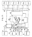
- FIG. 1 is a general block diagram of a system in which the system and method of the present invention may be implemented.
- This system has CPU 0 at 11, CPU 1 at 13, CPU 2 at 12, and CPU at 14. These CPUs are coupled to central unit 15. Central unit 15 will be described in detail subsequently.
- E-BUS 0 TA bus 17 connects CPU 0 at 11 to central unit 15
- E-BUS 1 TA bus 19 connects CPU 1 at 13 to central unit 15
- E-BUS 2 TA bus 18 connects CPU 2 at 12 to central unit 15
- E-BUS 3 TA bus 20 connects CPU 3 at 14 to central unit 15 (collectively, "E-BUS TA buses").
- E-BUS TA buses These uni-directional buses are for transmissions from the CPUs to central unit 15.
- E-BUS 0 FA bus 21 which connects CPU 0 at 11 to the central unit
- E-BUS 1 FA bus 23 which connects CPU 1 at 13 to the central unit
- E-BUS 2 FA bus 22 which connects CPU 2 at 12 to the central unit
- E-BUS 3 FA bus 24 which connects CPU 3 at 14 to central unit.
- Each of the CPUs also connect to an I/O bus adaptor 25 over two uni-directional buses. Each is a 16-bit bus. One bus is an input bus and the other is an output bus.
- control console 29 is associated with CPU 0 at 11. However, it is understood that it may be associated with more than one CPU.
- Central unit 15 is connected to shared memory 31 by uni-directional A-BUS FA 33 and uni-directional bus A-BUS TA 35.
- A-BUS FA 33 is for transmissions from the central unit to the shared memory 31.
- A-BUS TA 35 is for transmissions from shared memory 31 to the central unit.
- Shared memory 31 includes memory modules which are designated 31a, 31b, 31c, 31d, 31e, and 31f. Each memory module connects to central unit 15 via A-BUS FA at 33 and A-BUS TA at 35. It is to be understood that there may be more shared memory, or there may be more or less memory modules for a single shared memory and still be within the scope of the invention. It is further understood that each module may be of the same type of memory or each may be of a different type.
- E-BUS TA buses 17, 19, 18, and 20, E-BUS FA buses 21, 23, 22, and 24, and A-BUS FA bus 33 are 32-bit parallel buses, and A-BUS TA bus 35 is a 64-bit parallel bus.
- the central unit 15 performs two basic functions. First, it combines the signals input to it from the CPU and memory on the E-BUS TA and A-BUS TA buses, respectively, so that they are provided as outputs on the output buses E-BUS FA and A-BUS FA. Second, it contains a memory controller for memory modules 31a-31f. Central unit 15 also controls system timing. This is done through a central clock which is not shown.
- Figure 2 is a block diagram of the system shown in Figure 1, with the first implementation of the present invention in the system shown in Figure 1.
- OR gates are used to combine the point to point signals from E-BUS TA buses 17, 19, 18, and 20 into a common signal.
- the 32-bit wide E-BUS TA buses 17, 19, 18, and 20 connect to the series of OR gates 37 and 41.
- OR gates 37 and 41 For simplicity of description only single lines as shown for the 32-bit wide buses and only one series of OR gates are shown for handling these buses. It is understood, however, that in actuality there would be 32 series of OR gates 37 and 41 to accommodate the 32-bits of the buses. It is further understood that the single 32-bit wide output of OR gate 37 is input to memory controller 45 and OR gate 41, and the single 32-bit wide output of OR gate 41 is input to state device 42. With this understanding Figure 2 will now be discussed.
- E-BUS 0 TA 17 from CPU 0 at 11 connects to a first input to OR gate 37
- E-BUS 1 TA bus 19 from CPU 1 at 13 connects to the second input to gate 37
- E-BUS 2 TA bus 18 from CPU 2 at 12 connects to the third input of OR gate 37
- E-BUS 3 TA bus 20 from CPU 3 at 14 connects to the fourth input to OR gate 37.
- the output of OR gate 37 is bus 36 which is the first input to OR gate 41. Bus 36 is also input to memory controller 45.
- the second input to OR gate 41 is the output from memory controller 45.
- the output of OR gate 41 on bus 39 is input to the data input of state device 42. When state device 42 receives the input from OR gate 41, it stores the output for one cycle before providing it at its output.
- This arbitration logic which can be centrally located or in one or more of the CPUs is necessary to ensure that only one of the CPUs has access to the bus 36 at a time. This logic functions on a request/request granted type of operation.
- state device 42 After passing through driver 43, is input to CPU 0 at 11, CPU 1 at 13, CPU 2 at 12, and CPU 3 at 14 via E-BUS 0 FA bus 21, E-BUS 1 FA bus 23, E-BUS 2 FA bus 22, and E-BUS 3 FA bus 24, respectively. It is understood that the output to the state device is a 32-bit wide output.
- OR gate 37 bus 36
- the second input to OR gate 41 is the output of memory controller 45. Therefore, the refill data from memory 31 that is on the A-BUS TA bus 35 passes through memory controller 45 for input to the second input of OR gate 41. This data is later caused to be input to state device 42. After processing by the state device, the refill data is supplied to the CPUs via driver 43 and the E-BUS FA buses. This is how refill data operates for a read.
- FIG 3 is a simplified block diagram of a second implementation of the present invention incorporated in the system shown at Figure 1.
- multiplexers (“MUXes") replace the series of OR gate.
- MUXes 37a and 41a replace the OR gates.
- logic element 50 is also added.
- Port logic 49 is disposed at the input to MUX 37a.
- the buffer in port logic 49 can hold up to three words, the number of words being a function of the length of time for the CPU's to recognize a bus grant condition from one of the E-BUS TA buses.
- Logic element 50 processes these bits and provides selection inputs to MUXes 37a and 41a.
- FIG 4 is a more detailed block diagram of the central unit 15 of Figure 3.
- Logic element 50 in Figure 3 includes as part thereof port select logic 65 that is shown in Figure 4.
- Port select logic 65 is combined with multiplexer 37a to form scheduling logic 66.
- Resource check logic 67 combines with MUX 41a and state device 42 to form arbitrator 51.
- E-BUS 0 TA bus 17, E-BUS 1 TA bus 19, E-BUS 2 TA bus 18, and E-BUS 3 TA bus 20 connect to port logic 49.
- Each of these E-BUS TA buses from one of the CPUs is connected to its own port of port logic 49.
- E-BUS 0 TA bus 17 connects to port 49a
- E-BUS 1 TA 19 connects to port logic 49b.
- E-BUS TA buses Four types of information may be communicated on the E-BUS TA buses. These types are: (1) data, commands and address information ("DAL"); (2) FC information, which are signals to indicate whether the information on the DAL lines is a command, or address or data; (3) "snoopy hit” information, which indicates that a CPU associated with that bus has a "snoopy hit;” and (4) parity information.
- DAL data, commands and address information
- FC information which are signals to indicate whether the information on the DAL lines is a command, or address or data
- "snoopy hit” information which indicates that a CPU associated with that bus has a "snoopy hit
- parity information parity information.
- each of the CPUs may include a cache memory. These memories may be used to speed up access to data which is being used extensively by a CPU. Thus, each time a read command is sent out, each CPU checks to see if the associated address is in its cache. In a manner that will be explained in more detail below, this operation which is known as a "snoopy" operation, is done with timing that insures that any response to a "snoopy” read, which is a “snoopy hit,” takes place before refill data returns from one of the memory modules in memory 31.
- the information on buses E-BUS 0 TA bus 17, E-BUS 1 TA bus 19, E-BUS 2 TA bus 18, and E-BUS 3 TA bus 20 is input to state device 53.
- the output of the state device 53 is coupled to MUX 59 and to buffer 55.
- Buffer 55 can store up to three words of predetermined length.
- the output of the state device 53 is also input to validity logic 57.
- the second input to validity logic 57 is a signal that is fed back from the output of validity logic 57.
- the other output of validity logic 57 connects to the selection inputs of MUX 59.
- the PORT GRANT signal on line 61 which is output from arbitrator 51, is also input to validity logic 57.
- validity logic 57 is to determine if commands and data are valid, and which of the data, either in buffer 55 or input directly to port MUX 59, are to be switched onto bus 63 at the output port MUX 59.
- the output of port MUX 59 on bus 63 is input to MUX 37a.
- the output of port MUX 59 on bus 63 is also input to port select logic 65.
- MUX 37a and port select logic 65 are part of scheduling logic 66.
- Port select logic 65 in response to outputs from the arbitrator 51, selects one of the four inputs to MUX 37a to be coupled to the output of that MUX. This is coordinated with the operation of validity logic 57 which controls the output of port MUX 59 on bus 63. Port select logic 65 grants the four ports supplying inputs to bus 63 access to bus 36 on a round robin basis.
- Output bus 36 is input to resource check logic block 67 of the arbitrator 51, MUX 41a, and a number of other units.
- These units are memory map unit (“MMAP") 69, lock logic unit (“LOCK”) 71, input/output unit (“CPIO”) 73, interrupt request unit (“IREQ/SNIT”) 75, memory controller (“MEMC/DBEC”) 77, and memory write data path unit (“MWDP”) 79.
- MMAP memory map unit
- LOCK lock logic unit
- CPIO input/output unit
- IREQ/SNIT interrupt request unit
- MEMC/DBEC memory controller
- MWDP memory write data path unit
- Resource check 67 receives status inputs from MMAP 69, LOCK 71, CPIO 73, IREQ/SNIT 75, MEMC/DBEC memory controller 77, and MWDP 79. These are the memory module status, the lock register status, the I/O module status, the error status, the memory controller status, and the write buffer status messages. In addition, the resource check logic block 67 generates ARB commands for input to the MUX 41a and a ARB MUX SELECT command for selecting which input will be output from MUX 41a for input to state device 42.
- A-BUS TA 35 is a 64-bits wide bus.
- the signals on that bus include DAL information, ECC (error correction code) information, and ACK (acknowledgement) information.
- the ACK bit is processed by memory read data path ("MRDP") 81.
- MRDP memory read data path
- the output of MRDP 81 which includes the DAL and ECC information is input to MEMC/DBEC 77.
- the DAL information here is generally refill data.
- the output of MEMC/DBEC is the refill data and this output is one of the inputs to MUX 41a.
- MEMC/DBEC 77 also provides an output on A-BUS FA bus 33.
- This output includes the DAL, ECC, FC, and parity information.
- This information on A-BUS FA bus 33 is input to memory modules 31a-31f.
- the output of MUX 41a through the state device 42 includes the same information that MEMC/DBEC 77 put on A-BUS FA 33 except that the ECC information is not included.
- resource check logic 67 uses the status information input from MMAP 69, LOCK 71, CPIO 73, IREQ/SNIT 75, MEMC/DBEC 77, and MWDP 79 to arbitrate between the different inputs to determine which input will be given access to E-BUS TA buses 21-24 through MUX 41a and state machine 42.
- the signals that desire access to these buses are the RSCK DAL and RSCK FC signals on bus 36, MMAP LW RD DAL signal output from MMAP 69, LOCK LW RD DAL signal output from LOCK 71, the CPIO LW RD DAL signal output from CPIO 73, the IREQ/SNIT LW RD DAL output from IREQ/SNIT 75, and the METL REFILL DAL signal output from MEMC/DBEC 77.
- Resource check logic 67 controls access to these buses via the output lines coupled through state devices 67a and 67b and the ARB MUX SELECT signal output from resource check logic 67.
- the outputs from state device 67a on line 61 and 85 are for controlling access of E-BUS TA bus information onto bus 36.
- the outputs from state device 67b on lines 83 are for causing selected DAL information from MMAP 69, LOCK 71, CPIO 73, IREQ/SNIT 75, and MEMC/DBEC 77 to be input to MUX 41a.
- FIG. 5 is a more detailed block diagram of the scheduling logic 66 of Figure 4.
- the scheduling logic includes as major elements port select logic 65 and MUX 37a.
- the output of the port logic 49 on bus 63 is input to scheduling logic 66.
- This input includes the port DAL signals, the port FC signals, the port "snoopy hit” signals, and the port CMD VALID (command valid) signals.
- the selection of which of these signals will be output from port logic 49 is determined by validity logic 57.
- lines 87 of bus 63 carry the port "snoopy hit" signals. These signals are inputs to priority encoder 89 and OR gate 91. The output of priority encoder 89 is input to MUX 403. The output of OR gate 91 is input to port select generator 93.
- Lines 96 of bus 63 carry the DAL and FC signals. These signals are the inputs to MUX 37a. The FC lines signals are also input to OLD FC MUX 95.
- Lines 97 of bus 63 carry the port CMD VALID signals. These signals are inputs to barrel shifter 99.
- the output of barrel shifter 99 is input to priority encoder 401.
- the 4-bit output of priority encoder 401 is one of the inputs to MUX 403. This 4-bit output is also input to left shift one block 405.
- the output of left shift one block 405 is one of the inputs to MUX 407.
- MUX 407 has state device 409 disposed at its output. The output of state device 409 feeds back as the second 4-bit input to the MUX 407 and as a 4-bit control input to barrel shifter 99.
- the first 4-bit input to MUX 403 is a feed back signal from state device 411. This is the last input to MUX 403.
- the 4-bit output of MUX 403 is input to state device 411.
- the 4-bit output of state device 411 is also input to the selection inputs of OLD FC MUX 95 which has as inputs the FC signals from lines 96 of bus 63.
- the output of MUX 95 on line 419 is the OLD FC signal. This is an input to port select generator 93 along with the output of OR gate 91 and two other inputs. These two other inputs are the SCHD GRANT signal on line 85a and SNOOPY HIT SHADOW signal on line 85b. Both of these signals are output from state device 67a of arbitrator 51. These signals are for controlling access of the E-BUS TA buses to bus 36.
- the first output of port select generator 93 is the selection input of MUX 403.
- the second output is input to the selection input of MUX 407.
- the control of these two MUXes determines the content of the output from MUX 37a on bus 36 and what the 4-bit SCHD ID signal on line 86 will be.
- the output of MUX 403 is input to the selection input of MUX 37a whose output is bus 36.
- priority encoder 401 prioritizes the ports with the highest priority being output first from the priority encoder on line 413 as the "current port” signal. This is also input to left shift one block 405. The output of the left shift one block is the next port in the sequence. So, the output of the left shift one block is the "next port” signal, which is input to MUX 407. The other input to MUX 407 through state device 409 is a feed back signal. This signal also connects to the control inputs to barrel shifter 99. Hence, the signal will cause the barrel shifter to point to the port associated with this signal. The signal that usually is at the feed back loop is the "current port”. This is true until changed by the selection of the "next port”.
- priority encoder 401 determines that port "0" should have access to bus 36 first.
- the 4-bit output of priority encoder 401 is input to left shift one block 405 and, as such, will shift left shift one block to indicate the next port which according to a normal sequence would be port "1.”
- the output of left shift one block 405 is loaded into the second input to a MUX 407.
- the first input to MUX 407 is the current port, which is port "0,” and is the present output of MUX 407 and latched in state device 409. This signal is fed back to an input of MUX 407.
- the state device continues to feed back port “0” until the port "0" information has been fully transmitted. This is controlled by port select generator 93 continuing to select the feed back input until port "0" has completed placing its data on bus 36.
- port select generator 93 selects the second input to MUX 407 which is the output of left shift one block 405. This will now provide the "next port,” port “1,” at the output of MUX 407. On the next cycle, the "next port” signal will be output from state device 409 and fed back to the first input to MUX 407.
- this value designating port 1 When this value designating port 1 is output from state device 409, it is also input to the barrel shifter 99.
- the new port designation signal advances the barrel shifter by one, so long as the "next port" in the normal sequence order has a valid port CMD VALID signal. If the next port in sequence is not valid, the barrel shifter advances to the next valid port.
- the output of the barrel shifter 99 is input to priority encoder 401 which now provides an output representative of the new port. As such, the newly selected port becomes the "current port” and a new "next port” is selected in the above described manner. This method of operation would continue with each port having its turn in round robin fashion.
- Each command is usually followed by at least one word.
- This word may be an address, or data (in the case of a refill). This address or data may be followed by additional data (in the case of a write command), a refill command, or a SWAP command (a combined read and write command).
- a port Once a port is given access to the bus, it must continue to be given access until it is finished transmitting its commands or data onto bus 36. For example, in the case of a SWAP command, the port must have continuous access to send the SWAP command, a read address, a write back command, a write address, and then the write data.
- FC changes states according to what is on the DAL lines. If it is a command, it has one state and the other state if it is not a command.
- the purpose of the MUX 403 is to select between a "previous port”, a "snoopy port", and the "current port”. As stated, it is only when predetermined events take place that the "previous port” or "snoopy port” inputs to MUX 403 are selected. The method of selecting the output of MUX 403 will now be discussed.
- the output of MUX 403 is input to the selection inputs of MUX 37a. This determines which port is granted access to bus 36. Normally, the output of MUX 403 is the "current port”; hence the “current port” is selected at MUX 37a. The "current port” is also input to state device 411. On the clock cycle after the "current port” is input state device 411, with the output therefrom on line 417. This output is input to the selection inputs of OLD FC MUX 95 and fed back as the "previous port” put to MUX 403.
- the FC signal will change states. This new state will be input to port select generator 93. This will cause the SCHD MODE SELECT (scheduling mode selector) output of the generator to have a bit pattern that will select the "previous port” input to MUX 403 which is latched in state device 411. The "previous port” value will remain as the output of MUX 403 until the state of the FC signal on line 419 changes signifying the end of data and the presence of a new command. It is only then that port select generator 93 will change its selection signals to select the "current port” rather than the "previous port.” This action ensures that data transmission in complete before another command is placed on bus 36.
- the "next port” value is selected at MUX 407. This is done by port select generator 93 changing which output the selection signals selects to be output from MUX 407. Once selected, the "next port” signal, through state device 409, is fed back to MUX 407 and barrel shifter 99. Barrel shifter 99 then selects the next valid port, which now becomes the "current port” on line 413.
- the scheduling logic 66 now awaits the next change in the state of the selected FC signal for repeating these actions. As an example of the operation of scheduling logic 66, the following is provided.
- this "current port” signal makes the selection of the "current port” DAL and FC at MUX 37a.
- this port designation i.e., port "0” is available at the output of state device 411.
- the output of state device 411 selects the corresponding port FC signal to be output from MUX 95.
- the FC bit for port “0” will be output from MUX 95 and fed back to port select generator 93.
- the FC bit for example, may be a logic "1" value.
- the FC bit On the second cycle, when other than a command is transmitted, it will change to a logic "0" value.
- a “snoopy hit shadow” is a time which covers the period required to obtain signals back from the CPUs when there has been a “snoopy hit”. That is, once a read command is put out on the bus, there is a certain amount of time before a signal will come back indicating a "snoopy hit", i.e., the requested data is in a CPU cache. If there is a "snoopy hit", a "snoopy refill command" will occur so the identified data may be provided.
- FIG. 6 is a more detailed block diagram of resource check logic 67. Referring to this Figure and Figure 5, the method for generating of a SNOOPY HIT SHADOW signal will be discussed.
- a "snoopy shadow” period is started.
- One of the outputs of command and resource check 427 is the “snoopy shadow start” signal on line 425. This signal is input to multistage shift register 429. The outputs of shift register 429 are combined in OR gate 431. The output of OR gate 431 is fed back to the command and resource check 427 and also is output from resource check logic 67 on line 85b as the SNOOPY HIT SHADOW signal.
- priority encoder 89 If there are more than one "snoopy hit", priority encoder 89 outputs a signal indicative of the "snoopy" port that has been assigned the highest priority.
- OR gate 91 When there has been a "snoopy hit" identified, the output of OR gate 91 will change state.
- port select generator 93 now selects the correct "snoopy" port for access to the bus 36 through MUX 403 and MUX 37a. That is, the "snoopy port” output from priority encoder 89 will be coupled to the output of MUX 403. This output will select the port corresponding to the correct "snoopy hit" for output through MUX 37a. The selected “snoopy port” will then send out its refill data on bus 36.
- command and resource check 427 (not shown), which is part of resource check logic 67, receives status inputs from MMAP 69, LOCK 71, CP10 73, IREQ/SNIT 75, MEMC/DBEC 77, and MWDP 79.
- the command from scheduling logic 66 that has been decoded by command decoder 435 is also input to command and resource check 427.
- This command may be from a particular CPU or port wishing to put a command and address on bus 36.
- the memory module status outputs from MMAP 69 have the most impact.
- memory modules 31a-31f there are a number of memory modules (memory modules 31a-31f).
- a second read command is not placed on the bus for the same memory module to which a prior active read command has been directed until a predetermined time period has passed. This time period includes memory latency and the time that it takes the memory to provide the refill data.
- command and resource check 427 decodes commands and their associated addresses to determine if it can grant the port requesting access, access to the memory bus based on the number of commands then pending and the availability of a specific memory module.
- the ARB MUX SELECT (arbitration multiplexer select) output is input to the selection inputs to MUX 41a.
- the inputs to MUX 41a are the RSCK DAL and RSCK FC from bus 36, the MMAP LW RD DAL signals from MMAP 69, LOCK LW RD DAL signals from LOCK 71, CP10 LW RD DAL signals CP10 73, IREQ/SNIT LR WD IREQ/SNIT signals 75, and MCTL REFILL DAL signals from MEMC/DBEC 77.
- important for consideration in the present invention is the selection between the RSCK DAL signal output from scheduling logic 66 on bus 36 and the MCTL refill data output from MEMC/DBEC 77. This will be discussed in greater detail with respect to Figure 10.
- FIG 7 a timing diagram for a read command is shown.
- CPU 1 is sending out a read command.
- CPU 1 sends read command 101 followed by address 103 at the second cycle.
- the command is arbitrated as indicated at 105.
- the arbitration will be between the CPUs competing for access to bus 36.
- the read command is loaded into the first buffer location of buffer 55 and the read address is loaded into the second buffer location of that buffer (see Figure 4).
- Buffer 55 can hold up to three words in its three buffer locations, but only two of those locations are used here.
- the CPU 1 port is granted access to bus 36 as shown at 107 of Figure 7. This is done by coupling the read command in the first buffer location of buffer 55 (See Figure 4) to bus 36 through MUXes 59 and 37a. This command is then coupled through MUX 41a reaching E-BUS FA buses 21-24.
- the address from the second buffer location of buffer 55 in port logic 49 is put on bus 36 as indicated at 111.
- the read command at 101 which the CPU put on one of the E-BUS TA buses during the first cycle, appears on each of the E-BUS FA buses 21-24 during the third cycle. In this way, the CPU which sent the original command will know, as will all of the other CPUs, that the request has been granted and that the requesting CPU has been given access to bus 36. This is done without the necessity of making a separate communication to each CPU.
- the read command and address at 101 and 103, respectively are provided to each of the other CPUs so that they may determine if they have the requested information in their caches for the purpose of a "snoopy hit.”
- the first piece of data is sent on a third cycle. The remainder of the data is provided in subsequent cycles.
- the write command and address will be processed in the same manner as a read command and address. The data, however, will be written to memory and not returned.
- FIG 8 is a timing diagram for "snoopy" refill command timing. Referring to this Figure, the processing of "snoopy hits" will be discussed. As stated, a "snoopy hit” occurs when a CPU has the address associated with a read command in its cache memory. The CPU that has the data in its cache responds to the read command by putting out a "snoopy refill” command followed by refill data on its E-BUS TA bus.
- refill command 201 is output from a CPU and input to the first buffer location of buffer 55 ( Figure 4), then a predetermined number cycles of refill data are output.
- the data is output at a rate of one byte per cycle.
- the first byte of refill data 203 is output at the second cycle and this first byte is input to the second buffer location of buffer 55 ( Figure 4)
- second byte 205 at the third cycle is input to the third buffer location of buffer 55 ( Figure 4)
- third byte 207 at the fourth cycle is held at state device 53 ( Figure 4).
- the remainder of the data is output at subsequent cycles.
- the refill command is latched in state device 42.
- This refill command indicated at 209, is transferred from the first buffer location.
- the refill data "0" at 211 is transferred from the second buffer location in buffer 55 and the refill data "1" at 213 is transferred from the third buffer location.
- the refill data "2" is transferred into the state device 42. It, therefore, is ready for output on the E-BUS FA at the next cycle, as shown at 215.
- the CPU that sent the refill command and refill data knows to begin sending data again beginning at seventh cycle, as indicated by refill data 217.
- the refill command was placed on E-BUS FA buses 21-24 at the fifth cycle, as indicated at 209.
- the CPU 3 read this data and at seventh cycle began sending data again.
- refill data 2 at 207 appears 3 bytes long instead of one byte.
- This data at 271 appears on the bus 36 just after data 215 as shown.
- the remaining refill data is passed through without the use of the buffer.
- the use of the buffer and the bus system of the present invention assures that, once the bus is granted to a CPU, there is a continuous flow of data and commands.
- FIG. 9 shows the timing for a SWAP command.
- SWAP command 301 is input to the first buffer location of buffer 55 at the first cycle and read address at 303 is input to the second buffer location at the second cycle.
- a write back command at 305 is input to the third buffer location of buffer 55 at the third cycle.
- the write back address at 307 is held on E-BUS TA bus 18, for example, for CPU 2. The reason it was held here will be explained subsequently.
- This diagram shows a one cycle late arbitration.
- the SWAP command appears on the E-BUS FA buses 21-24 at 311 followed by the read address at 313. Similar to the situation in Figure 5, the sending CPU knows that access has been granted and thus, beginning at sixth cycle time, it can begin sending data again as shown at 315. At this time, the one cycle late arbitration problem is corrected.
Landscapes
- Engineering & Computer Science (AREA)
- Computer Hardware Design (AREA)
- Theoretical Computer Science (AREA)
- Physics & Mathematics (AREA)
- Software Systems (AREA)
- General Engineering & Computer Science (AREA)
- General Physics & Mathematics (AREA)
- Mathematical Physics (AREA)
- Bus Control (AREA)
- Multi Processors (AREA)
Description
Claims (33)
- A bus system, comprising:characterized by:(a) a plurality of bus elements including a plurality of central processing units (CPU0, ..., CPU3) and a shared memory (31);(b) a central unit (15) having a plurality of bus inputs and an output, with the central unit coupling at least one of the inputs to the output;(c) a first plurality of uni-directional point-to-point buses (17, 18, 19, 20, 33) coupling the bus elements to the central unit bus inputs;(d) a second plurality of uni-directional point-to-point buses (21, 22, 23, 24, 35) coupling the output of the central unit to each of the bus elements; and(e) arbitration logic (50) granting the bus elements access through the central unit one at a time.
- A system as recited in claim 1, wherein the system further includes a state device (42) that is disposed at the output of the central unit (15) for storing said output for one cycle before providing it at its output.
- A system as recited in claim 2, wherein the central unit comprises OR logic comprising at least one OR gate (37), and the arbitration logic grants the bus elements access to associated first buses.
- A system as recited in claim 2, wherein the central unit includes a multiplexer (37a).
- A system as recited in claim 4, wherein the system further includes a flip-flop (42) as a state device at each input to the central unit, with the state devices also being connected to the arbitration logic (50).
- A system as recited in claim 5, wherein the arbitration logic (50) is part of the central unit (15).
- A system as recited in claim 6, wherein the arbitration logic includes a scheduler (66) and an arbiter (51).
- A system as recited in one of claims 1 to 7, wherein the shared memory further comprises a plurality of memory modules (31a, ..., 31f) with a single one of the first buses and a single one of the second buses being provided for coupling to the memory.
- A system as recited in claim 3, wherein the OR logic, comprises:a first OR gate (37) which has as inputs the first buses from the plurality of central processing units, with the output of the first OR gate being coupled to the second bus for the shared memory (31); anda second OR gate (41) which has as a first input the output of the first OR gate (37) and as a second input the first bus from the shared memory (31), with the output of the second OR gate (41) being coupled to the second buses to the central processing unit.
- A system as recited in claim 9, wherein the system further includes a state device (42) that is connected to the output of the second OR gate (41), with the output of the state device (42) being connected to the second buses leading to the central processing units.
- A system as recited in claim 10, wherein the system further includes at least one driver (43) between the output of the state device (42) and the second buses leading to the central processing units.
- A system as recited in claim 1, wherein in the central unit (15) includes multiplexer circuits (37a, 41a) and arbitration logic (50) for controlling the multiplexers.
- A system as recited in claim 12, wherein the multiplexer logic, comprises:a first multiplexer (37a) which has as inputs a first bus from each of the central processing units and providing an output coupled to the second bus from the central unit (15) to the shared memory (31); anda second multiplexer (41a) which has as a first input the output of the first multiplexer (37a) and as a second input the first bus from the shared memory (31) to the central unit (15), with the output of the second multiplexer (41a) being connected to each of the second buses leading to the central processing units.
- A system as recited in claim 13, wherein the system further includes a first state device (42) at the output of the second multiplexer (41a), with the output of the first state device (42) being connected to the second buses leading to the central processing units.
- A system as recited in claim 14, wherein the system further includes at least one driver (43) between the output of the first state device (42) and the second buses leading to the central processing units.
- A system as recited in claim 15, wherein the central unit further includes a memory controller (45), with the memory controller (45) providing at its output the second bus to the memory and having as an input the first bus from the memory, with the memory controller (45) connecting the first bus to the second multiplexer (41a) and connecting the output of the first multiplexer (37a) to the second bus.
- The system as recited in claim 16, wherein the system further includes port logic (49) that connects each of the first buses from the central processing unit to the first multiplexer (37a).
- The system as recited in claim 17, wherein for each input port coupled to one of the first buses, the port logic (49) includes:an input state device (53);a buffer (55) having a plurality of locations, the input of the buffer (55) coupled to the output of the input state device (53);a port multiplexer (59) having as inputs the outputs of the buffer locations (55) and the output of the input state device (53); andvalidity logic (57) having as inputs the output of the state device and a control input from the arbitration logic for granting the port access to the bus system, with the validity logic providing an output to control the port multiplexer (59).
- The system as recited in claim 18, wherein the arbitration logic includes an arbitrator (51) and scheduling logic (66).
- The system as recited in claim 19, wherein the outputs of the port multiplexers (59) in the port logic for each of the central processing units is connected to the inputs of the first multiplexer (37a), with the port select logic comprising logic responsive to the outputs of the port multiplexers and to an input from the arbitrator to control the first multiplexer (37a) such as to selectively couple one of its inputs to its output.
- The system as recited in claim 20, wherein the scheduling logic (66) includes logic to grant the input ports access on a round robin basis.
- A system as recited in claim 3, wherein said port select logic comprises:a barrel shifter (199);a first priority encoder (401) having as inputs the outputs of the barrel shifter (199);a schedule port ID multiplexer (403) having as a first input the output of the priority decoder;left shift one logic (405) having an input coupled to the output of the first priority encoder (401) and providing an output which is left shifted by one;a next port multiplexer (407) having as a first input the output of the left shift one logic;a second state device (409) coupled to the output of the next port multiplexer, the output of the state device coupled back as a second input to next port multiplexer and as an input to the barrel shifter (199);a third state device (411) at the output of the schedule port ID multiplexer (403) providing its output as a second input to the schedule port ID multiplexer, the output of the schedule port ID multiplexer (403) also coupled to control the first multiplexer; andport select logic for controlling the schedule port ID multiplexer (403) to switch between the input of the priority encoder (401) and the fed back input from the third state device.
- The system as recited in claim 22, wherein each of the first buses includes at least one FC line indicative of the beginning and end of a transmission on the bus and the port select logic is responsive to the control line to switch the schedule port ID multiplexer (403) to the next port.
- The system as recited in claim 23, wherein the port select logic includes an old FC multiplexer (95) having as inputs the FC lines from each of the ports, with the FC multiplexer being controlled by the output of the third state device (411); and
a port select generator (93) having as one input the output of the old FC multiplexer and as a second input a scheduler grant input from the arbitrator. - The system as recited in claim 24, wherein at least some of the central processing units include cache memory with each of the first buses including a "snoopy hit line" indicating that the addresses in a read command issued by another central processing unit are contained within its cache memory, with the port schedule logic further comprising:a second priority encoder (89) having as inputs the "snoopy hit lines" from the buses;an OR gate (91) having as inputs said "snoopy hit lines", the output of the OR gate providing an input to the port select generator (93); andthe port select generator (93) having as a further input a "snoopy hit shadow signal" indicating the period during which "snoopy hit signals" may occur, the output of the second priority encoder (89) designating a "snoopy port" at which a "snoopy hit" has occurred and being coupled as a third input to the schedule port ID multiplexer (403), the port select generator (93), in response to receiving to the "snoopy hit signal" within the period of the "snoopy hit shadow" selects as the port to which access is to be granted, the "snoopy port" designated at the output of the priority encoder (401).
- The system as recited in claim 25, wherein the central unit (15) further includes at least one resource status unit including a memory map status unit indicating the status of modules in the shared memory (31), with the arbitrator including a resource check logic (427) having as inputs the outputs from the resource status units, the output of the first multiplexer and the output of the memory controller, the resource checker responsive thereto to provide outputs to the port logic and to the port select logic in the schedule logic (66) and also to provide an output to the second multiplexer (41a) to select between resources, the resources including data from one of the central processing units at the output of the first multiplexer (37a) and memory data from the shared memory modules (31a, ..., 31f).
- The system as recited in claim 26, wherein the resource check logic includes a command decoder (435) receiving as an input the output from the first multiplexer; anda command and resource check module (427) having as one input the output of the command decoder (435) and as additional inputs the outputs of the units indicating the status of modules of the shared memory; anda timing circuit (429) for generating the "snoopy hit shadow".
- A system according to claim 1 comprising:
said central unit (15), including:combining logic for accepting a plurality of inputs at least equal to the number of the central processing units plus memory and coupling at least one of inputs to its output;arbitration logic (50) for controlling which of the inputs is provided at the output;a memory controller (45) providing a memory input to the combining logic and receiving a memory output from the combining logic;a plurality of first uni-directional point-to-point buses (17, 18, 19, 20), with one bus coupling each of the central processing units to an input of the combining logic;a first uni-directional memory bus (33) coupling the memory to the memory controller;a plurality of second uni-directional point-to-point buses (21, 22, 23, 24) coupling the output of the combining logic to the central processing units; anda second uni-directional memory bus (35) coupling the output of the memory (31) to the memory control logic. - A system as recited in claim 28, wherein the combining logic comprises two stages of combining logic, a first stage of combining logic having the first buses from the central processing units as inputs and providing its output to the memory controller (45); and
a second stage of combining logic having as inputs the output of the first stage of combining logic and the output of the memory controller (45), with the output of the second stage of combining logic being provided to the second buses coupled to the plurality of central processing units. - A system as recited in claim 29, wherein the first and second stages of combining logic comprise first (37a) and second (41a) multiplexers, and the arbitration logic (50) comprises logic for controlling the multiplexers.
- A method of implementing a high speed bus to which a plurality of bus elements including a plurality of central processing units (CPU0, ..., CPU3) and a shared memory (31) are coupled, characterized by comprising the steps of:(a) coupling each of the bus elements to a central unit (15) with a separate first uni-directional bus (17, 18, 19, 20, 33) having a direction from the bus elements to the central unit;(b) selecting one of the first bus inputs to the central unit (15) to be an output; and(c) coupling said output to each of the bus elements over a separate second uni-directional bus (21, 22, 23, 24, 35) having a direction from the central unit to the bus elements.
- The method as recited in claim 31, wherein the selecting step further comprises selecting between the inputs on the first buses from the central processing unit and the bus from the memory (31).
- The method as recited in claim 32, wherein the central processing units (CPU0, ..., CPU3) output commands requesting access to the memory (31), each command followed by an address and/or data and/or additional commands and further including:storing up to three words output by a central processing unit at the central unit (15);arbitrating access to the bus at the output of the central unit (15), including granting access to one of the central processing unit inputs by providing the stored command to the output and on successive cycles providing additional words stored at the central unit on the output; andwhen all stored words have been provided on the output on the next and subsequent cycles providing any input words from the central processing unit directly on the output whereby, by storing a number of words in the central unit, once the central processing unit is granted access to the bus, a continual flow of data will occur without any dead time.
Applications Claiming Priority (2)
| Application Number | Priority Date | Filing Date | Title |
|---|---|---|---|
| US54654790A | 1990-06-29 | 1990-06-29 | |
| US546547 | 1990-06-29 |
Publications (2)
| Publication Number | Publication Date |
|---|---|
| EP0464708A1 EP0464708A1 (en) | 1992-01-08 |
| EP0464708B1 true EP0464708B1 (en) | 1998-06-10 |
Family
ID=24180912
Family Applications (1)
| Application Number | Title | Priority Date | Filing Date |
|---|---|---|---|
| EP19910110755 Expired - Lifetime EP0464708B1 (en) | 1990-06-29 | 1991-06-28 | High speed bus system |
Country Status (5)
| Country | Link |
|---|---|
| EP (1) | EP0464708B1 (en) |
| JP (1) | JPH04280347A (en) |
| AU (1) | AU636739B2 (en) |
| CA (1) | CA2042711A1 (en) |
| DE (1) | DE69129566T2 (en) |
Families Citing this family (8)
| Publication number | Priority date | Publication date | Assignee | Title |
|---|---|---|---|---|
| GB2285524B (en) * | 1994-01-11 | 1998-02-04 | Advanced Risc Mach Ltd | Data memory and processor bus |
| US5754865A (en) * | 1995-12-18 | 1998-05-19 | International Business Machines Corporation | Logical address bus architecture for multiple processor systems |
| FR2759472B1 (en) * | 1997-02-12 | 1999-05-07 | Thomson Csf | FAST SEMAPHORE REGISTER WITH SECURE OPERATION WITHOUT SPECIFIC BUS PROTOCOL |
| US6732255B1 (en) * | 1999-09-15 | 2004-05-04 | Koninklijke Philips Electronics N.V. | Can microcontroller that permits concurrent access to different segments of a common memory by both the processor core and the DMA engine thereof |
| JP4198376B2 (en) * | 2002-04-02 | 2008-12-17 | Necエレクトロニクス株式会社 | Bus system and information processing system including bus system |
| KR100464036B1 (en) * | 2002-09-07 | 2005-01-03 | 엘지전자 주식회사 | Information exchange apparatus for multiprocessor |
| JP4249741B2 (en) * | 2005-11-04 | 2009-04-08 | Necエレクトロニクス株式会社 | Bus system and information processing system including bus system |
| CN114036091B (en) * | 2021-10-30 | 2023-06-16 | 西南电子技术研究所(中国电子科技集团公司第十研究所) | Multiprocessor peripheral multiplexing circuit and multiplexing method thereof |
Family Cites Families (3)
| Publication number | Priority date | Publication date | Assignee | Title |
|---|---|---|---|---|
| DE3340123A1 (en) * | 1983-11-05 | 1985-05-15 | Helmut Dipl.-Inform. 5860 Iserlohn Bähring | Communications unit for coupling microcomputers |
| WO1987004826A1 (en) * | 1986-02-10 | 1987-08-13 | Eastman Kodak Company | Multi-processor apparatus |
| JPH02115962A (en) * | 1988-10-26 | 1990-04-27 | K S D:Kk | System for connecting computer device to its peripheral device |
-
1991
- 1991-04-23 AU AU75281/91A patent/AU636739B2/en not_active Ceased
- 1991-05-16 CA CA 2042711 patent/CA2042711A1/en not_active Abandoned
- 1991-06-11 JP JP13918791A patent/JPH04280347A/en active Pending
- 1991-06-28 EP EP19910110755 patent/EP0464708B1/en not_active Expired - Lifetime
- 1991-06-28 DE DE1991629566 patent/DE69129566T2/en not_active Expired - Fee Related
Also Published As
| Publication number | Publication date |
|---|---|
| CA2042711A1 (en) | 1991-12-30 |
| DE69129566D1 (en) | 1998-07-16 |
| JPH04280347A (en) | 1992-10-06 |
| AU636739B2 (en) | 1993-05-06 |
| DE69129566T2 (en) | 1998-12-17 |
| AU7528191A (en) | 1992-03-26 |
| EP0464708A1 (en) | 1992-01-08 |
Similar Documents
| Publication | Publication Date | Title |
|---|---|---|
| US6928500B1 (en) | High speed bus system that incorporates uni-directional point-to-point buses | |
| US5870625A (en) | Non-blocking memory write/read mechanism by combining two pending commands write and read in buffer and executing the combined command in advance of other pending command | |
| US5404464A (en) | Bus control system and method that selectively generate an early address strobe | |
| US5754800A (en) | Multi processor system having dynamic priority based on row match of previously serviced address, number of times denied service and number of times serviced without interruption | |
| US5202973A (en) | Method of controlling a shared memory bus in a multiprocessor system for preventing bus collisions and for ensuring a full bus | |
| US4481572A (en) | Multiconfigural computers utilizing a time-shared bus | |
| US5819105A (en) | System in which processor interface snoops first and second level caches in parallel with a memory access by a bus mastering device | |
| US6026464A (en) | Memory control system and method utilizing distributed memory controllers for multibank memory | |
| US5685005A (en) | Digital signal processor configured for multiprocessing | |
| US6006307A (en) | Computer system employing a mirrored memory system for providing prefetch bandwidth | |
| US5619720A (en) | Digital signal processor having link ports for point-to-point communication | |
| US4763249A (en) | Bus device for use in a computer system having a synchronous bus | |
| US4769768A (en) | Method and apparatus for requesting service of interrupts by selected number of processors | |
| AU598857B2 (en) | Move-out queue buffer | |
| EP0139569A2 (en) | Arbitration mechanism for assigning control of a communications path in a digital computer system | |
| JP2002140289A (en) | Microcontroller DMA operation with adjustable word size transfer and address alignment / increment | |
| KR100644596B1 (en) | Bus system and its bus arbitration method | |
| JPH0810447B2 (en) | How to maintain data compatibility of all physical addresses used by memory sharing multiprocessors | |
| EP0464708B1 (en) | High speed bus system | |
| US5537609A (en) | Mini cache operational module for enhancement to general cache | |
| US7130946B2 (en) | Configuration and method having a first device and a second device connected to the first device through a cross bar | |
| EP0139568A2 (en) | Message oriented interrupt mechanism for multiprocessor systems | |
| AU606083B2 (en) | Interface between processor and special instruction processor in digital data processing system | |
| US5696938A (en) | Computer system permitting mulitple write buffer read-arounds and method therefor | |
| EP0340347B1 (en) | Bus arbitration system |
Legal Events
| Date | Code | Title | Description |
|---|---|---|---|
| PUAI | Public reference made under article 153(3) epc to a published international application that has entered the european phase |
Free format text: ORIGINAL CODE: 0009012 |
|
| 17P | Request for examination filed |
Effective date: 19910729 |
|
| AK | Designated contracting states |
Kind code of ref document: A1 Designated state(s): DE FR GB IT NL |
|
| 17Q | First examination report despatched |
Effective date: 19961016 |
|
| GRAG | Despatch of communication of intention to grant |
Free format text: ORIGINAL CODE: EPIDOS AGRA |
|
| GRAG | Despatch of communication of intention to grant |
Free format text: ORIGINAL CODE: EPIDOS AGRA |
|
| GRAH | Despatch of communication of intention to grant a patent |
Free format text: ORIGINAL CODE: EPIDOS IGRA |
|
| GRAH | Despatch of communication of intention to grant a patent |
Free format text: ORIGINAL CODE: EPIDOS IGRA |
|
| GRAA | (expected) grant |
Free format text: ORIGINAL CODE: 0009210 |
|
| AK | Designated contracting states |
Kind code of ref document: B1 Designated state(s): DE FR GB IT NL |
|
| REF | Corresponds to: |
Ref document number: 69129566 Country of ref document: DE Date of ref document: 19980716 |
|
| ITF | It: translation for a ep patent filed | ||
| PGFP | Annual fee paid to national office [announced via postgrant information from national office to epo] |
Ref country code: GB Payment date: 19980724 Year of fee payment: 8 |
|
| ET | Fr: translation filed | ||
| PLBE | No opposition filed within time limit |
Free format text: ORIGINAL CODE: 0009261 |
|
| STAA | Information on the status of an ep patent application or granted ep patent |
Free format text: STATUS: NO OPPOSITION FILED WITHIN TIME LIMIT |
|
| PGFP | Annual fee paid to national office [announced via postgrant information from national office to epo] |
Ref country code: NL Payment date: 19990531 Year of fee payment: 9 |
|
| PGFP | Annual fee paid to national office [announced via postgrant information from national office to epo] |
Ref country code: FR Payment date: 19990601 Year of fee payment: 9 |
|
| 26N | No opposition filed | ||
| PGFP | Annual fee paid to national office [announced via postgrant information from national office to epo] |
Ref country code: DE Payment date: 19990603 Year of fee payment: 9 |
|
| PG25 | Lapsed in a contracting state [announced via postgrant information from national office to epo] |
Ref country code: GB Free format text: LAPSE BECAUSE OF NON-PAYMENT OF DUE FEES Effective date: 19990628 |
|
| GBPC | Gb: european patent ceased through non-payment of renewal fee |
Effective date: 19990628 |
|
| PG25 | Lapsed in a contracting state [announced via postgrant information from national office to epo] |
Ref country code: NL Free format text: LAPSE BECAUSE OF NON-PAYMENT OF DUE FEES Effective date: 20010101 |
|
| PG25 | Lapsed in a contracting state [announced via postgrant information from national office to epo] |
Ref country code: FR Free format text: LAPSE BECAUSE OF NON-PAYMENT OF DUE FEES Effective date: 20010228 |
|
| NLV4 | Nl: lapsed or anulled due to non-payment of the annual fee |
Effective date: 20010101 |
|
| REG | Reference to a national code |
Ref country code: FR Ref legal event code: ST |
|
| PG25 | Lapsed in a contracting state [announced via postgrant information from national office to epo] |
Ref country code: DE Free format text: LAPSE BECAUSE OF NON-PAYMENT OF DUE FEES Effective date: 20010403 |
|
| PG25 | Lapsed in a contracting state [announced via postgrant information from national office to epo] |
Ref country code: IT Free format text: LAPSE BECAUSE OF NON-PAYMENT OF DUE FEES;WARNING: LAPSES OF ITALIAN PATENTS WITH EFFECTIVE DATE BEFORE 2007 MAY HAVE OCCURRED AT ANY TIME BEFORE 2007. THE CORRECT EFFECTIVE DATE MAY BE DIFFERENT FROM THE ONE RECORDED. Effective date: 20050628 |