EP0459366A2 - Contrast correction device - Google Patents
Contrast correction device Download PDFInfo
- Publication number
- EP0459366A2 EP0459366A2 EP91108616A EP91108616A EP0459366A2 EP 0459366 A2 EP0459366 A2 EP 0459366A2 EP 91108616 A EP91108616 A EP 91108616A EP 91108616 A EP91108616 A EP 91108616A EP 0459366 A2 EP0459366 A2 EP 0459366A2
- Authority
- EP
- European Patent Office
- Prior art keywords
- contrast
- signal
- correction
- gamma correction
- circuit
- Prior art date
- Legal status (The legal status is an assumption and is not a legal conclusion. Google has not performed a legal analysis and makes no representation as to the accuracy of the status listed.)
- Granted
Links
Images


Classifications
-
- H—ELECTRICITY
- H04—ELECTRIC COMMUNICATION TECHNIQUE
- H04N—PICTORIAL COMMUNICATION, e.g. TELEVISION
- H04N5/00—Details of television systems
- H04N5/14—Picture signal circuitry for video frequency region
- H04N5/20—Circuitry for controlling amplitude response
-
- H—ELECTRICITY
- H04—ELECTRIC COMMUNICATION TECHNIQUE
- H04N—PICTORIAL COMMUNICATION, e.g. TELEVISION
- H04N5/00—Details of television systems
- H04N5/44—Receiver circuitry for the reception of television signals according to analogue transmission standards
- H04N5/57—Control of contrast or brightness
Definitions
- the luminance signal S1 is shown as a waveform of negative going signal.
- the positive/negative gamma correction circuit 5 comprises one or more, such as three in the example shown in Fig. 2, slice circuits 9a, 9b, and 9c, and a voltage divider defined by a plurality of resistors connected in series between a line carrying pedestal voltage Vj and a line carrying white peak voltage Vk to produce reference voltages Vq, Vr and Vs. Note that Vq ⁇ Vr ⁇ Vs.
- an adder circuit 12 adds the control correction signal Sp and luminance signal S1 to produce the post-correction luminance signal S2a, which is also shown in three different conditions using real line, dotted line and dot-dash line.
- the dotted line corresponds to the case shown in Fig. 5e in which the positive gamma correction is obtained;
- the real line corresponds to the case shown in Fig. 5a in which the negative gamma correction is obtained;
- the dot-dash line corresponds to the case shown in Fig. 5c in which no gamma correction is obtained.
- the white peak detection signal S6 when the white peak detection signal S6 is smaller than the low threshold VL, (i.e., when the image itself is considered to be dark), the contrast of light or white tone areas is suppressed for the better enhancement of dark tone areas as shown in Fig. 5e.
- the white peak detection signal S6 is between the low and high thresholds VL and VH, a linear characteristics are applied as shown in Fig. 5c.
- the white peak detection signal S6 is greater than the high threshold VH (i.e., when the image itself is considered to be bright), the contrast of light tone areas is enhanced as shown in Fig. 5a.
Landscapes
- Engineering & Computer Science (AREA)
- Multimedia (AREA)
- Signal Processing (AREA)
- Picture Signal Circuits (AREA)
- Processing Of Color Television Signals (AREA)
- Television Receiver Circuits (AREA)
- Telephonic Communication Services (AREA)
Abstract
Description
- The present invention relates to a television receiver and, more particularly, to a contrast correction device which can be used to correct contrast in a video signal in a television receiver, a video cassette recorder, or the like.
- As the screen size of color television receivers has increased in recent years contrast correction devices have become increasingly important as a means of expanding the dynamic range of the video signal reproduced on the CRT screen by correcting the contrast of the video signal for a sharper image by passing the video signal through a non-linear amplifier such as a gamma correction device.
- One type of such device is a described below with reference to the accompanying figures.
- Figs. 6, 7a and 7b are, respectively, a block diagram and graphs showing the input/output relationship in a first example of a conventional contrast correction device. As shown in Fig. 6, the contrast correction device comprises a
gamma correction circuit 1 which corrects the luminance signal S1 input thereto so as to suppress white or bright tones according to an average detected luminance signal S3'; an averageluminance detection circuit 2 which averages the luminance signal S2' over one or a plurality of frames and produces an average detected luminance signal S3'; and amatrix circuit 3 which adds the luminance signal S2' and an input color difference signal S4 to output the color signal S5' to CRT 4. - A contrast correction device thus constructed operates as described below.
- First, the post-correction luminance signal S2' is input to the average
luminance detection circuit 2 for averaging the signal S2' over a predetermined time which may be more than one vertical scan period to detect the average luminance signal S3'. The detected average luminance signal S3' is input to thegamma correction circuit 1. Thegamma correction circuit 1 changes the input-output characteristics according to the average detected luminance signal S3' as shown in Figs. 7a and 7b. - More specifically, when the average detected luminance signal S3' is of dark, white or light tones are suppressed and black tones are enhanced as shown in Fig. 7a. On the contrary, when the average detected luminance signal S3' is of bright image, suppression of white or light ones is weakened as shown in Fig. 7b so that white or light tones are enhanced more than that resulted from the case shown in Fig. 7a. The post-correction luminance signal S2' thus obtained input to the
matrix circuit 3 to be added with the input color difference signal S4, resulting in generation of the color signal S5' to drive theCRT 4 to generate the video image. - Figs. 8, 9a and 9b are, respectively, a block diagram and graphs showing the input-output characteristics according to a second example of a conventional contrast correction device. When compared with the example shown in Fig. 6, the contrast correction device shown in Fig. 8 has, in place of the average
luminance detection circuit 2, a white peaklevel detection circuit 6 which detects the whitest level of the post-correction luminance signal S2'' to output a white peak signal S6', and a whitepeak comparison circuit 7 which compares the white peak detection signal S6' with a predetermined white peak level signal Vg' set externally and outputs the result as a white peak comparison signal S8'. - A contrast correction device of Fig. 10 operates as described below.
- First, the post-correction luminance signal S2'' is input to the white peak
level detection circuit 6 to detect the white peak level (the luminance of the whitest part of the video signal) over a predetermined time which may be more than one vertical scan period. The detected white peak level is output as the white peak detection signal S6' (the level of which increases as the white peak level increases) and compared by the whitepeak comparison circuit 7 with an externally set white peak level voltage Vg', thus yielding the white peak comparison signal S8', which is input to thegamma correction circuit 1. - The
gamma correction circuit 1 changes the input-output characteristics as shown in Figs. 9a and 9b according to the white peak comparison signal S8'. When the voltage level of the white peak level voltage Vg' is equal to or greater than the white peak detection signal S6' (i.e., when the image is dark overall), the light tones are suppressed as shown in Fig. 9a to enhance the dark tones. When the white peak level voltage Vg' is less than the white peak detection signal S6' (i.e., when the image is bright overall), correction is suppressed as shown in Fig. 8b for better enhancement of the light tones when compared with Fig. 9a. The post-correction luminance signal S2'' thus obtained is input to thematrix circuit 3 where it is added to the input color difference signal S4 to generate the color signal S5'', which is then used to drive theCRT 4 and generate the video image. - However, with conventional contrast correction devices as described above, when the average luminance is bright in the first example, or the white peak detection signal S6' level is high (bright) in the second example, the gamma input-output characteristics of light or white tones are simply made approximately linear. This does not make it possible to expand the dynamic range, resulting in the need to further expand the dynamic range to achieve a high image quality in large-screen television displays.
- The object of the present invention is therefore to provide a contrast correction device which solves these problems.
- The present invention has been developed with a view to substantially solving the above described disadvantages and has for its essential object to provide an improved contrast correction device.
- In order to achieve the aforementioned objective, a contrast correction device for correcting a contrast of an image formed by video signals by varying a luminance signal, comprises a brightness detecting means for detecting whether or not the image is brighter than a predetermined brightness; and a correction means for correcting the luminance signal by a negative gamma correction when the image is detected as brighter than the predetermined brightness, whereby contrast of bright image areas in the image are enhanced.
-
- These and other objects and features of the present invention will become clear from the following description taken in conjunction with the preferred embodiments thereof with reference to the accompanying drawings throughout which like parts are designated by like reference numerals, and in which:
- Fig. 1 is a block diagram of a contrast correction device according to a first embodiment of the present invention;
- Fig. 2 is a block diagram of a positive/negative gamma correction circuit shown in Fig. 1;
- Fig. 3 is a graph showing waveforms of signals observed at various places in the contrast correction device shown in Fig. 2;
- Fig. 4 is a block diagram of a contrast correction device according to a second embodiment of the present invention;
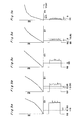
- Figs. 5a, 5b, 5c, 5d, and 5c are graphs showing the input-output characteristics observed in various conditions;
- Fig. 6 is a block diagram of a first example of a conventional contrast correction device;
- Figs. 7a and 7b are graphs showing the input-output characteristics observed in the contrast correction device shown in Fig. 6;
- Fig. 8 is a block diagram of a second example of a conventional contrast correction device; and
- Fig. 9a and 9b are graphs showing the input-output characteristics observed in the contrast correction device shown in Fig. 8.
- Referring to Fig. 1, a contrast correction device according to a first embodiment of the present invention is shown. The contrast correction device comprises a positive/negative
gamma correction circuit 5 for correcting the of luminance signal S1 according to the average luminance signal S3 as described below. When the average luminance signal S3 is relatively low indicating that the image is dark, the positive gamma correction characteristics is applied for contrast correction whereby the contrast of light or white tones in the luminance signal S1 is suppressed for the better enhancement of dark tones. When the average detected luminance signal S3 is bright, negative gamma correction characteristics are applied for contrast correction whereby the contrast of light tones is enhanced as will be described in detail later. The averageluminance detection circuit 2,matrix circuit 3, andCRT 4 are the same as those used in the conventional contrast correction device described hereinabove. - The average
luminance detection circuit 2 receives the post-correction signal S2 and takes an average over one or a number of frames to produce an average luminance signal S3 as shown in Figs. 5a to 5e. The average luminance signal S3 is then input to the positive/negativegamma correction circuit 5. - When the detected average luminance is low (dark), such as in the case of Fig. 5e, the average luminance signal S3 will be relatively low, such as -C in which C=1 according to the present embodiment. In response to signal S3, which is -C in this case, the positive gamma correction is carried out in the positive/negative
gamma correction circuit 5 so as to establish the input/output characteristics of thegamma correction circuit 5 that bends downward as shown in Fig. 5e in a manner which will be described in detail later. Thus the contrast of bright (white) tone areas is suppressed for the better enhancement of the dark tone areas. - When the detected average luminance is a medium contrast, such as in the case of Fig. 7c, the average luminance signal S3 will take an intermediate level, such as 0. In response to signal S3, which is 0 in this case, no gamma correction is carried out in the positive/negative
gamma correction circuit 5 so as to establish the input/output characteristics of thegamma correction circuit 5 that extends straight as shown in Fig. 5c. - When the detected average luminance is high (bright) such as in the case of Fig. 7a, the average luminance signal S3 will be relatively high, such as +C. In response to signal S3, which is +C in this case, the negative gamma correction is carried out in the positive/negative
gamma correction circuit 5 so as to establish the input/output characteristics of thegamma correction circuit 5 that bends upward as shown in Fig. 7a. Thus the contrast of light (white) tone areas is enhanced. - When the detected average luminance is slightly low or slightly high, the average luminance signal S3 will be at corresponding levels, such as -0.5C or +0.5C, as shown in Figs. 5d or 5b, respectively. In such cases, the input/output characteristics of the
correction circuit 5 will be slightly bent upwards or downwards as shown in Figs. 5d and 5b, respectively. - Referring to Fig. 2, a detailed block diagram of the positive/negative
gamma correction circuit 5 is shown. The luminance signal S1 is shown as a waveform of negative going signal. The positive/negativegamma correction circuit 5 comprises one or more, such as three in the example shown in Fig. 2,slice circuits Vs. Slice circuit 9a compares the input luminance signal S1 with the predetermined reference voltage Vq which is between voltages Vj and Vk and produces an output Sℓ corresponding to a portion of the input luminance signal S1 that has exceeded the reference voltage Vq, as shown in Fig. 3. Similarly,slice circuit 9b produces an output Sm corresponding to a portion of the input luminance signal S1 that has exceeded the reference voltage Vr andslice circuit 9c produces an output Sn corresponding to a portion of the input luminance signal S1 that has exceeded the reference voltage Vs. - An
adder 10 is provided for adding the compared luminance signals Sℓ, Sm, and Sn to produce a correction signal So, as shown in Fig. 3. The correction signal So is amplified in again control circuit 11, the gain of which is controlled by the average luminance signal S3 to be between -C and +C. Thus, gaincontrol circuit 11 produces a control correction signal Sp, as shown in Fig. 3, in which the real line is obtained when S3=+C, dotted line is obtained when S3=-C, and dot-dash line is obtained when S3=0. Then, anadder circuit 12 adds the control correction signal Sp and luminance signal S1 to produce the post-correction luminance signal S2a, which is also shown in three different conditions using real line, dotted line and dot-dash line. The dotted line corresponds to the case shown in Fig. 5e in which the positive gamma correction is obtained; the real line corresponds to the case shown in Fig. 5a in which the negative gamma correction is obtained; and the dot-dash line corresponds to the case shown in Fig. 5c in which no gamma correction is obtained. - It is to be noted that an negative gamma input-output characteristics are obtained when the gain of the
gain control circuit 11 is negative, and a positive gamma input--output characteristics are obtained when the gain is positive. In the present embodiment, the input-output characteristics are varied by the use of threeslice circuits - According to the contrast correction device of the present embodiment, it is possible to obtain positive gamma input-output characteristics when the average value is dark and negative gamma input-output characteristics when the average value is bright. Thus, when the averaged brightness level of one or several image frames has a relatively high level, the contrast of the light tone areas will be enhanced. On the other hand, when the average brightness level of one or several image frames has a relatively low level, the contrast of the dark tone areas will be enhanced.
- An alternative embodiment of the present invention will be described hereinbelow with reference to the accompanying figures.
- Referring to Fig. 4, a block diagram of a contrast correction device according to a second embodiment of the present invention is shown. According to the second embodiment, the average
luminance detecting circuit 2 is replaced with a white peaklevel detection circuit 6 which produces a which produces a white peak detection signal S6 as shown in Figs. 5a-5e. The white peak detection signal S6 is compared in acomparator 8 with a high threshold voltage VH and a low threshold voltage VL. - When the white peak detection signal S6 is greater than the high threshold voltage VL, a signal S8 produced from
comparator 8 is in a high level, such as +C. Thus, the negative gamma input-output characteristics is established in the positive/negativegamma correction circuit 5 in a similar manner described above. This condition is shown in Fig. 5a. - When the white peak detection signal S6 is smaller than the low threshold voltage VL, the signal 8a from
comparator 8 is in a low level, such as -C. Thus, the negative gamma input-output characteristics is established in the positive/negativegamma correction circuit 5 in a similar manner described above. This condition is shown in Fig. 5e. - When the white peak detection signal S6 is between the high and low threshold voltages VH and VL, the signal 8a from
comparator 8 is in an intermediate level, such as 0. Thus, no gamma correction is added to the characteristic line in the positive/negativegamma correction circuit 5. This condition is shown in Fig. 5c. - In other words, according to the second embodiment, when the white peak detection signal S6 is smaller than the low threshold VL, (i.e., when the image itself is considered to be dark), the contrast of light or white tone areas is suppressed for the better enhancement of dark tone areas as shown in Fig. 5e. When the white peak detection signal S6 is between the low and high thresholds VL and VH, a linear characteristics are applied as shown in Fig. 5c. When the white peak detection signal S6 is greater than the high threshold VH (i.e., when the image itself is considered to be bright), the contrast of light tone areas is enhanced as shown in Fig. 5a.
- Thus, the contrast of light tone areas (dynamic range) can be extended by suppressing the contrast of light or white tone areas to enhance the contrast of dark tone areas when the white peak level is low (dark), and enhancing the contrast of light or white tone areas when the white peak level is relatively high (bright).
- It is to be noted that in the first embodiment of the present invention the input signal to the average
luminance detection circuit 2 is the post-correction luminance signal S2b, but the luminance signal S1 may also be input thereto. - Furthermore, in the second embodiment of the present invention the input signal of the white peak
level detection circuit 6 is the post-correction luminance signal S2b, but the luminance signal S1 may also be input thereto. - According to the contrast correction device it is possible to extend the dynamic range of a video signal on the white contrast region by providing a positive/negative gamma correction circuit in the contrast correction device.
- It is more effective to provide a gain control device in a stage before the positive/negative
gamma correction circuit 5 so as to control the rising angle ϑ of input-output characteristics line relative to the darkness of the image. - Although the present invention has been fully described in connection with the preferred embodiments thereof with reference to the accompanying drawings, it is to be noted that various changes and modifications are apparent to those skilled in the art. Such changes and modifications are to be understood as included within the scope of the present invention as defined by the appended claims unless they depart therefrom.
Claims (15)
- A contrast correction device for correcting a contrast of an image formed by video signals by varying a luminance signal, comprising:
brightness detecting means (2, 6) for detecting whether or not said image is brighter than a predetermined brightness; and
correction means (5) for correcting said luminance signal by a negative gamma correction when said image is detected as brighter than said predetermined brightness, whereby contrast of bright image areas in said image are enhanced. - A contrast correction device as claimed in claim 1, further comprising:
darkness detecting means (2, 6) for detecting whether or not said image is darker than a predetermined darkness; and
correction means (5) for correcting a luminance signal by a positive gamma correction when said image is detected as darker than said predetermined darkness, whereby contrast of bright image areas in said image are suppressed. - A contrast correction device for correcting a contrast of an image formed by video signals by varying a luminance signal, comprising:
brightness/darkness detecting means (2, 6) for detecting a tone level of said image and for producing a bright signal when said tone level is greater than a predetermined brightness, and a dark signal when said tone level is less than a predetermined darkness; and
correction means (5) for correcting a luminance signal (S1) by a negative gamma correction in response to said bright signal, and a positive gamma correction in response to said dark signal, whereby contrast of bright image areas in said image are enhanced when said bright signal is produced, and the same are suppressed when said dark signal is produced. - A contrast correction device as claimed in Claim 3, wherein said brightness/darkness detecting means (2, 6) is an average detection means (2) for detecting an average of said luminance signal (S1, S2a, or S2b) over a predetermined time to produce an average luminance signal (S3).
- A contrast correction device as claimed in Claim 4, wherein said predetermined time is at least one frame period.
- A contrast correction device for controlling a contrast of an image formed by video signals by varying a luminance signal, comprising:
an average detection circuit (2) for detecting an average luminance level of a video signal; and
a positive/negative gamma correction circuit (5) for correcting the contrast of a video signal, such that the contrast in bright image areas is enhanced by changing the correction of said positive/negative gamma correction circuit according to the output of said average detection circuit (2) in such a manner that positive gamma correction is strengthened when the average luminance is low and positive gamma correction is changed to negative gamma correction when the average luminance is high. - A contrast correction device as claimed in claim 6 is employed in a television receiver.
- A contrast correction device for controlling a contrast of an image formed by video signals by varying a luminance signal, comprising:
a white peak level detection circuit (6) for detecting the white peak level of a video signal, and
an negative gamma correction circuit (5) for correcting the contrast of a video signal, such that the correction of the negative gamma correction circuit (5) is adjusted according to the output of the white peak level detection circuit (6) in such a manner that negative gamma correction is strengthened when the white peak level is high and negative gamma correction is reduced or eliminated when the white peak level is low. - A contrast correction device as claimed in claim 8 is employed in a television receiver.
- A contrast correction device for controlling a contrast of an image formed by video signals by varying a luminance signal (S1), comprising:
a white peak level detection circuit (6) for detecting the white peak level of a video signal; and
an positive/negative gamma correction circuit for correcting the contrast of a video signal, such that the correction of said positive/negative gamma correction circuit is adjusted according to the output of the white peak level detection circuit (6) in such a manner that positive gamma correction is strengthened when the white peak level is low and positive gamma correction is reduced when the white peak level is high, and when the white peak level is high gamma correction is also changed to negative gamma correction. - A contrast correction device as claimed in claim 10 is employed in a television receiver.
- A contrast correction device for controlling a contrast of an image formed by video signals by varying a luminance signal (S1), comprising:
an average detection circuit (2) for detecting an average luminance level of a video signal; and
at least one slice circuit (9a, 9b, and 9c) for slicing said input luminance signal comprising:
a voltage divider for dividing the potential difference between a pedestal voltage (Vj) of the video signal and a white peak voltage thereof;
an adder circuit (10) for adding the output signals from said slice circuit (9a, 9b, and 9c);
a gain control circuit (11) for controlling the gain of the output from said adder circuit (10) from a negative to a positive level according to said average luminance level and for producing a gain controlled signal (Sp); and
a subtracter for subtracting the gain controlled signal (Sp) from said luminance signal (S1), such that the contrast correction is changed from positive gamma correction characteristics to negative gamma correction characteristics according to the average value of the video signal. - A contrast correction device as claimed in claim 12 is employed in a television receiver.
- A contrast correction device for controlling a contrast of an image formed by video signals by varying a luminance signal (S1), comprising:
a white peak level detection circuit (6) for detecting the white peak level of said video signal; and
at least one slice circuit (9a, 9b, 9c) for slicing said input luminance signal (S1) comprising:
a voltage divider for dividing the potential difference between a pedestal voltage (Vj) of said video signal and a white peak voltage thereof;
an adder circuit (10) for adding the output signals (Sℓ, Sm, and Sn) from said slice circuit (9a, 9b, and 9c):
a gain control circuit (11) for controlling the gain of the output from said adder circuit (10) from a negative to a positive level according to the white peak level; and
a subtracter (12) for subtracting the gain controlled signal (Sp) from said luminance signal (S1), such that the contrast correction is changed from positive gamma correction characteristics to negative gamma correction characteristics according to the white peak level. - A contrast correction device as claimed in claim 14 is employed in a television receiver.
Priority Applications (1)
| Application Number | Priority Date | Filing Date | Title |
|---|---|---|---|
| EP95112922A EP0684733B1 (en) | 1990-05-31 | 1991-05-28 | Contrast correction device |
Applications Claiming Priority (2)
| Application Number | Priority Date | Filing Date | Title |
|---|---|---|---|
| JP143158/90 | 1990-05-31 | ||
| JP2143158A JPH0437263A (en) | 1990-05-31 | 1990-05-31 | Gradation correction device |
Related Child Applications (2)
| Application Number | Title | Priority Date | Filing Date |
|---|---|---|---|
| EP95112922.0 Division-Into | 1991-05-28 | ||
| EP95112922A Division EP0684733B1 (en) | 1990-05-31 | 1991-05-28 | Contrast correction device |
Publications (3)
| Publication Number | Publication Date |
|---|---|
| EP0459366A2 true EP0459366A2 (en) | 1991-12-04 |
| EP0459366A3 EP0459366A3 (en) | 1992-03-04 |
| EP0459366B1 EP0459366B1 (en) | 1996-08-14 |
Family
ID=15332271
Family Applications (2)
| Application Number | Title | Priority Date | Filing Date |
|---|---|---|---|
| EP95112922A Expired - Lifetime EP0684733B1 (en) | 1990-05-31 | 1991-05-28 | Contrast correction device |
| EP91108616A Expired - Lifetime EP0459366B1 (en) | 1990-05-31 | 1991-05-28 | Contrast correction device |
Family Applications Before (1)
| Application Number | Title | Priority Date | Filing Date |
|---|---|---|---|
| EP95112922A Expired - Lifetime EP0684733B1 (en) | 1990-05-31 | 1991-05-28 | Contrast correction device |
Country Status (8)
| Country | Link |
|---|---|
| US (1) | US5196937A (en) |
| EP (2) | EP0684733B1 (en) |
| JP (1) | JPH0437263A (en) |
| KR (1) | KR960001027B1 (en) |
| AU (1) | AU630810B2 (en) |
| CA (1) | CA2043325C (en) |
| DE (2) | DE69121313T2 (en) |
| MY (1) | MY109715A (en) |
Cited By (6)
| Publication number | Priority date | Publication date | Assignee | Title |
|---|---|---|---|---|
| DE4237420A1 (en) * | 1992-01-14 | 1993-07-15 | Matsushita Electric Industrial Co Ltd | |
| DE4242275C1 (en) * | 1992-01-22 | 1993-10-07 | Matsushita Electric Industrial Co Ltd | Tint control circuit and associated gradient matching circuit |
| EP0570873A3 (en) * | 1992-05-22 | 1994-02-16 | Thomson Consumer Electronics | |
| EP0585558A3 (en) * | 1992-09-01 | 1996-11-20 | Matsushita Electric Industrial Co Ltd | Video signal processor |
| GB2400765A (en) * | 2003-04-18 | 2004-10-20 | Hitachi Ltd | Luminance-dependent video display control |
| US7034896B2 (en) | 2001-05-31 | 2006-04-25 | Matsushita Electric Industrial Co., Ltd. | Gradation correction apparatus |
Families Citing this family (17)
| Publication number | Priority date | Publication date | Assignee | Title |
|---|---|---|---|---|
| JP4802350B2 (en) * | 1998-03-12 | 2011-10-26 | ソニー株式会社 | Display device |
| JP2800373B2 (en) * | 1990-05-31 | 1998-09-21 | 松下電器産業株式会社 | Automatic image quality adjustment device for magnetic recording and playback devices |
| JP2748678B2 (en) * | 1990-10-09 | 1998-05-13 | 松下電器産業株式会社 | Gradation correction method and gradation correction device |
| JPH0799861B2 (en) * | 1991-02-28 | 1995-10-25 | 松下電器産業株式会社 | Gradation correction circuit |
| CA2095756C (en) * | 1992-08-14 | 2001-04-24 | Albert D. Edgar | Method and apparatus for linear color processing |
| DE4231611A1 (en) * | 1992-09-22 | 1994-03-24 | Thomson Brandt Gmbh | Method and device for monitoring an alternating signal |
| US5719965A (en) * | 1994-12-13 | 1998-02-17 | Hewlett-Packard Company | Higher precision look-up table from lower precision look-up table for improved tonal adjustment |
| US5734362A (en) * | 1995-06-07 | 1998-03-31 | Cirrus Logic, Inc. | Brightness control for liquid crystal displays |
| JPH08336062A (en) * | 1995-06-08 | 1996-12-17 | Sony Corp | Television receiver |
| KR0185136B1 (en) * | 1996-02-21 | 1999-04-15 | 김광호 | VCR Image Clarity Enlarger |
| GB2321155B (en) * | 1996-12-30 | 1999-09-22 | Lg Electronics Inc | Video input level control circuit in a video appliance |
| DE69908713T2 (en) * | 1998-06-22 | 2004-05-13 | Texas Instruments Inc., Dallas | Selective brightness expansion |
| DE19845187A1 (en) * | 1998-10-01 | 2000-04-13 | Loewe Opta Gmbh | Method for adjusting the brightness of a cell on a flat display |
| US6633343B2 (en) | 2000-03-14 | 2003-10-14 | Matsushita Electric Industrial Co., Ltd. | Dynamic gamma correction apparatus |
| JP4893902B2 (en) * | 2001-03-21 | 2012-03-07 | 株式会社一宮電機 | Ring jig holding jig, set jig and punching jig, and electrostatic powder coating method using them |
| KR100601654B1 (en) * | 2004-01-08 | 2006-07-14 | 삼성전자주식회사 | Apparatus and method for improving the quality of input video |
| JP4241492B2 (en) * | 2004-04-28 | 2009-03-18 | ブラザー工業株式会社 | Image forming apparatus |
Family Cites Families (15)
| Publication number | Priority date | Publication date | Assignee | Title |
|---|---|---|---|---|
| US3684825A (en) * | 1971-02-19 | 1972-08-15 | Rca Corp | Contrast compression circuits |
| JPS4989429A (en) * | 1972-12-26 | 1974-08-27 | ||
| GB1524720A (en) * | 1976-09-16 | 1978-09-13 | Marconi Co Ltd | Contrast correction arrangements |
| JPS56107674A (en) * | 1980-01-31 | 1981-08-26 | Sony Corp | Gradation correcting device of video signal |
| JPS58500853A (en) * | 1980-11-14 | 1983-05-26 | サンタ・バ−バラ・リサ−チ・センタ− | Method and apparatus for growing mercury cadmium telluride by liquid phase epitaxy from a mercury-rich melt |
| JPS58125627A (en) * | 1982-01-21 | 1983-07-26 | Nippon Telegr & Teleph Corp <Ntt> | Preparation of infrared transmission optical fiber preform by inside casting |
| JPH0411432Y2 (en) * | 1985-03-30 | 1992-03-23 | ||
| GB8521019D0 (en) * | 1985-08-22 | 1986-10-01 | Rank Pullin Controls Ltd | Imaging apparatus |
| JPH071854B2 (en) * | 1986-04-08 | 1995-01-11 | ソニー株式会社 | Non-linear companding circuit |
| JPS6478076A (en) * | 1987-09-18 | 1989-03-23 | Matsushita Electric Industrial Co Ltd | Signal correcting circuit |
| GB2211045B (en) * | 1987-10-10 | 1991-08-21 | Marconi Co Ltd | Linearity adjusting circuit |
| US4829381A (en) * | 1988-04-18 | 1989-05-09 | Polaroid Corporation | System and method for electronic image enhancement by dynamic pixel transformation |
| JP2591088B2 (en) * | 1988-07-22 | 1997-03-19 | 松下電器産業株式会社 | Video signal white compression device |
| US4980756A (en) * | 1989-08-25 | 1990-12-25 | Rca Licensing Corporation | Control signal generator for a television system |
| US5003394A (en) * | 1989-08-25 | 1991-03-26 | Rca Licensing Corporation | Dynamic video system including automatic contrast and "white-stretch" processing sections |
-
1990
- 1990-05-31 JP JP2143158A patent/JPH0437263A/en active Pending
-
1991
- 1991-05-27 AU AU77322/91A patent/AU630810B2/en not_active Ceased
- 1991-05-27 CA CA002043325A patent/CA2043325C/en not_active Expired - Fee Related
- 1991-05-28 EP EP95112922A patent/EP0684733B1/en not_active Expired - Lifetime
- 1991-05-28 DE DE69121313T patent/DE69121313T2/en not_active Expired - Fee Related
- 1991-05-28 DE DE69131143T patent/DE69131143T2/en not_active Expired - Fee Related
- 1991-05-28 EP EP91108616A patent/EP0459366B1/en not_active Expired - Lifetime
- 1991-05-29 US US07/707,003 patent/US5196937A/en not_active Expired - Fee Related
- 1991-05-30 MY MYPI91000948A patent/MY109715A/en unknown
- 1991-05-30 KR KR1019910008848A patent/KR960001027B1/en not_active Expired - Fee Related
Cited By (11)
| Publication number | Priority date | Publication date | Assignee | Title |
|---|---|---|---|---|
| DE4237420A1 (en) * | 1992-01-14 | 1993-07-15 | Matsushita Electric Industrial Co Ltd | |
| DE4237420C2 (en) * | 1992-01-14 | 1993-10-14 | Matsushita Electric Industrial Co Ltd | Image brightness control method and image brightness control circuit |
| DE4242275C1 (en) * | 1992-01-22 | 1993-10-07 | Matsushita Electric Industrial Co Ltd | Tint control circuit and associated gradient matching circuit |
| EP0570873A3 (en) * | 1992-05-22 | 1994-02-16 | Thomson Consumer Electronics | |
| US5422680A (en) * | 1992-05-22 | 1995-06-06 | Thomson Consumer Electronics, Inc. | Non-linear contrast control apparatus with pixel distribution measurement for video display system |
| EP0585558A3 (en) * | 1992-09-01 | 1996-11-20 | Matsushita Electric Industrial Co Ltd | Video signal processor |
| US7034896B2 (en) | 2001-05-31 | 2006-04-25 | Matsushita Electric Industrial Co., Ltd. | Gradation correction apparatus |
| GB2400765A (en) * | 2003-04-18 | 2004-10-20 | Hitachi Ltd | Luminance-dependent video display control |
| GB2400765B (en) * | 2003-04-18 | 2005-02-09 | Hitachi Ltd | Video signal processing circuit,video display apparatus,and video display method |
| US7265795B2 (en) | 2003-04-18 | 2007-09-04 | Hitachi, Ltd. | Video signal processing circuit, video display apparatus, and video display method |
| CN100397909C (en) * | 2003-04-18 | 2008-06-25 | 株式会社日立制作所 | Video signal processing circuit, video display device, and video display method |
Also Published As
| Publication number | Publication date |
|---|---|
| DE69121313D1 (en) | 1996-09-19 |
| EP0684733A3 (en) | 1996-01-10 |
| EP0684733B1 (en) | 1999-04-14 |
| DE69131143D1 (en) | 1999-05-20 |
| JPH0437263A (en) | 1992-02-07 |
| EP0684733A2 (en) | 1995-11-29 |
| EP0459366A3 (en) | 1992-03-04 |
| AU7732291A (en) | 1991-12-05 |
| MY109715A (en) | 1997-04-30 |
| US5196937A (en) | 1993-03-23 |
| EP0459366B1 (en) | 1996-08-14 |
| DE69121313T2 (en) | 1997-03-27 |
| AU630810B2 (en) | 1992-11-05 |
| CA2043325C (en) | 1996-02-20 |
| KR960001027B1 (en) | 1996-01-17 |
| CA2043325A1 (en) | 1991-12-01 |
| DE69131143T2 (en) | 1999-12-09 |
| KR910021116A (en) | 1991-12-20 |
Similar Documents
| Publication | Publication Date | Title |
|---|---|---|
| EP0684733B1 (en) | Contrast correction device | |
| JP4011122B2 (en) | Image quality correction circuit for video signals | |
| US7199840B2 (en) | Dynamic gray scale range adjustment apparatus and method | |
| US7394932B2 (en) | Video signal processor and method of processing video signal | |
| US4811101A (en) | Black level correction circuit for correcting black level of a video signal | |
| JP3208814B2 (en) | Video signal correction device | |
| KR100257940B1 (en) | Video system with feedback controlled "white stretch" processing and brightness compensation | |
| JPH03126377A (en) | Gradation correction device | |
| EP0467602A2 (en) | Contrast corrector for video signal | |
| US20040109091A1 (en) | Apparatus and method for adaptive brightness control | |
| US5396300A (en) | Contrast correction device for correcting video signal contrast by varying luminance signal | |
| KR970006659B1 (en) | Gradation compensating apparatus for a video signal | |
| US7675573B2 (en) | Global motion adaptive system with motion values correction with respect to luminance level | |
| US7471336B2 (en) | Global motion adaptive system with motion values correction with respect to luminance level | |
| KR100393219B1 (en) | Automatic beam limiter circuit | |
| JPH0690382A (en) | Gradation correction device | |
| JPH06350873A (en) | Television receiver | |
| JP3189319B2 (en) | High brightness adjustment device | |
| KR19980014689A (en) | Gamma correction device using histogram | |
| JP2003348378A (en) | Video signal processing circuit | |
| JPH04349785A (en) | Gradation correction device | |
| JPH0638074A (en) | Picture quality adjusting circuit | |
| JP2002278503A (en) | Image display device | |
| JP2000206923A (en) | Video signal processing device and image display device | |
| JPH10126646A (en) | Noise reduction circuit |
Legal Events
| Date | Code | Title | Description |
|---|---|---|---|
| PUAI | Public reference made under article 153(3) epc to a published international application that has entered the european phase |
Free format text: ORIGINAL CODE: 0009012 |
|
| 17P | Request for examination filed |
Effective date: 19910528 |
|
| AK | Designated contracting states |
Kind code of ref document: A2 Designated state(s): DE GB |
|
| PUAL | Search report despatched |
Free format text: ORIGINAL CODE: 0009013 |
|
| AK | Designated contracting states |
Kind code of ref document: A3 Designated state(s): DE GB |
|
| 17Q | First examination report despatched |
Effective date: 19940603 |
|
| GRAH | Despatch of communication of intention to grant a patent |
Free format text: ORIGINAL CODE: EPIDOS IGRA |
|
| GRAH | Despatch of communication of intention to grant a patent |
Free format text: ORIGINAL CODE: EPIDOS IGRA |
|
| GRAA | (expected) grant |
Free format text: ORIGINAL CODE: 0009210 |
|
| AK | Designated contracting states |
Kind code of ref document: B1 Designated state(s): DE GB |
|
| XX | Miscellaneous (additional remarks) |
Free format text: TEILANMELDUNG 95112922.0 EINGEREICHT AM 17/08/95. |
|
| REF | Corresponds to: |
Ref document number: 69121313 Country of ref document: DE Date of ref document: 19960919 |
|
| PLBE | No opposition filed within time limit |
Free format text: ORIGINAL CODE: 0009261 |
|
| STAA | Information on the status of an ep patent application or granted ep patent |
Free format text: STATUS: NO OPPOSITION FILED WITHIN TIME LIMIT |
|
| 26N | No opposition filed | ||
| REG | Reference to a national code |
Ref country code: GB Ref legal event code: IF02 |
|
| PGFP | Annual fee paid to national office [announced via postgrant information from national office to epo] |
Ref country code: GB Payment date: 20050525 Year of fee payment: 15 |
|
| PGFP | Annual fee paid to national office [announced via postgrant information from national office to epo] |
Ref country code: DE Payment date: 20050526 Year of fee payment: 15 |
|
| PG25 | Lapsed in a contracting state [announced via postgrant information from national office to epo] |
Ref country code: GB Free format text: LAPSE BECAUSE OF NON-PAYMENT OF DUE FEES Effective date: 20060528 |
|
| PG25 | Lapsed in a contracting state [announced via postgrant information from national office to epo] |
Ref country code: DE Free format text: LAPSE BECAUSE OF NON-PAYMENT OF DUE FEES Effective date: 20061201 |
|
| GBPC | Gb: european patent ceased through non-payment of renewal fee |
Effective date: 20060528 |