EP0458612B1 - Printing apparatus - Google Patents
Printing apparatus Download PDFInfo
- Publication number
- EP0458612B1 EP0458612B1 EP91304624A EP91304624A EP0458612B1 EP 0458612 B1 EP0458612 B1 EP 0458612B1 EP 91304624 A EP91304624 A EP 91304624A EP 91304624 A EP91304624 A EP 91304624A EP 0458612 B1 EP0458612 B1 EP 0458612B1
- Authority
- EP
- European Patent Office
- Prior art keywords
- allocation
- buffer
- reading
- writing
- address
- Prior art date
- Legal status (The legal status is an assumption and is not a legal conclusion. Google has not performed a legal analysis and makes no representation as to the accuracy of the status listed.)
- Expired - Lifetime
Links
Images


Classifications
-
- G—PHYSICS
- G06—COMPUTING OR CALCULATING; COUNTING
- G06K—GRAPHICAL DATA READING; PRESENTATION OF DATA; RECORD CARRIERS; HANDLING RECORD CARRIERS
- G06K15/00—Arrangements for producing a permanent visual presentation of the output data, e.g. computer output printers
- G06K15/02—Arrangements for producing a permanent visual presentation of the output data, e.g. computer output printers using printers
- G06K15/12—Arrangements for producing a permanent visual presentation of the output data, e.g. computer output printers using printers by photographic printing, e.g. by laser printers
- G06K15/128—Arrangements for producing a permanent visual presentation of the output data, e.g. computer output printers using printers by photographic printing, e.g. by laser printers generating or processing printable items, e.g. characters
-
- G—PHYSICS
- G06—COMPUTING OR CALCULATING; COUNTING
- G06K—GRAPHICAL DATA READING; PRESENTATION OF DATA; RECORD CARRIERS; HANDLING RECORD CARRIERS
- G06K15/00—Arrangements for producing a permanent visual presentation of the output data, e.g. computer output printers
- G06K15/02—Arrangements for producing a permanent visual presentation of the output data, e.g. computer output printers using printers
-
- G—PHYSICS
- G06—COMPUTING OR CALCULATING; COUNTING
- G06K—GRAPHICAL DATA READING; PRESENTATION OF DATA; RECORD CARRIERS; HANDLING RECORD CARRIERS
- G06K2215/00—Arrangements for producing a permanent visual presentation of the output data
- G06K2215/0002—Handling the output data
- G06K2215/0062—Handling the output data combining generic and host data, e.g. filling a raster
- G06K2215/0065—Page or partial page composition
Definitions
- the present invention relates to a printing apparatus capable of printing a page at a time.
- a photosensitive drum that has been charged is irradiated with a light source to form an electrostatic latent image, and toner is made to adhere to the electrostatic latent image for development, and the toner image is transferred to the recording medium.
- the electrophotographic printer is capable of printing a page at a time, so that it can be used as a page printer.
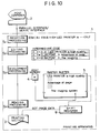
- Fig. 10 is a schematic diagram showing a conventional printing apparatus of this type.
- a host computer 2 is connected to a printing apparatus 1 via a parallel interface or a serial interface, and generating print data, and supplying the print data to the printing apparatus 1.
- the printing apparatus 1 When the print data is supplied from the host computer 2, the printing apparatus 1 performs reception processing (step S1), editing processing (step S2), development processing (step S3), and reading processing (step S4), to produce dot image data, and sends the dot image data to the printing section 3 of the electrophotographic printing system.
- the print data that have been received are in the form of code data such as "ESC(8U” (signifying designation of symbol set Roman-8); "ESC & K10H” (signifying character pitch 10 characters per inch); "LED PRINTER IS” (character series); "CR LF” (signifying return and line feed). These data are stored in a reception buffer, not shown.
- the editing is so made as to facilitate the development into the bit-map data in the subsequent step, and the edited data are stored in a page memory, not shown.
- designated font patterns are read from a font memory 4 in accordance with the intermediate codes in the page memory, and written into the designated locations in a raster buffer 5.
- the dot pattern data having been written in the raster buffer 5 are read by raster scan, and converted by a shift register 6 from the parallel data into serial data, and the data are then sent to the print section 3.
- the raster buffer 5 has a memory capacity for printout of one page, e.g., about 1 Mbytes in the case of a page of the letter size with a density of 300 dots per inch.
- the raster buffer 5 is either of the full-page buffer type in which reading is effected after development of data of one entire page is completed, and of the band-buffer type in which the limited memory capacity is divided into an area for dot pattern development and an area for reading, and these areas are used alternately for development and reading of one page.
- a printer with a band buffer comprising the features of the preamble of claim 1 is disclosed in JP-A-61 100 472.
- the present invention aims at solving the above problems, and providing a printing apparatus with which the cost increase due to the memory capacity for one page is avoided, it is not necessary to repeat the writing at the border of the raster buffer, it is possible to increase the printing speed, and the writing of dot patterns is not slower than the printing even when complicated patterns and a multiplicity of character patterns are concentrated in a specific region.
- a raster buffer for storing dot image data are divided into three layers in the direction of auxiliary scanning, and the respective layers are assigned to a writing layer in which font patterns read from a font memory are written, a reading layer from which dot image data that have been written are read, and a write-waiting layer in which those parts of font patterns that have overflown the writing layer are written.
- the writing layer and the write-waiting layer have a capacity for storing a character having the biggest size among those which are used frequently, e.g., a character of 12 points or greater size.
- font patterns Prior to printing of dot image data, font patterns are written in the writing layer and waiting layer, and the definition of the layer which has been the waiting layer is changed to a reading layer, dot image data are then read from the reading layer, the definition of the write-waiting layer waiting for the next writing is changed to a writing layer, and the definition of the reading layer from which the reading has been made is changed to a writing layer, with such change of definition being made successively.
- the printing apparatus according to the invention is set forth in claim 1.
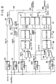
- Fig. 1 is a block diagram showing a printing apparatus of an embodiment of the invention.
- Fig. 2 is a schematic diagram of the raster buffer of the band buffer type.
- Fig. 3 is a flowchart showing the operation of the raster buffer.
- Fig. 4 is a diagram showing the memory layout of the printing apparatus according to the invention.
- Fig. 5 is a diagram showing the details of the raster buffer in the printing apparatus according to the invention.
- Fig. 6 is a diagram showing the dot pattern writing address circuit in the dot pattern development section.
- Fig. 7 is a diagram showing the dot pattern reading address circuit.
- Fig. 8 is a diagram showing a raster buffer of the three-allocation configuration.
- Fig. 9 is a diagram showing a raster buffer of the six-allocation configuration.
- Fig. 10 is a schematic diagram of a conventional printing apparatus.
- Fig. 1 is a block diagram showing an embodiment of the invention.
- a printing apparatus 1' and a host computer 2 are connected to each other.
- the printing apparatus comprises a printing section 3 of the electrophotographic printing system, and a microprocessor 7.
- a built-in initialization program memory 8 effects initialization and the like
- a built-in program memory 9 is for performing control over the printing apparatus.
- An initialization information memory 10 comprises a nonvolatile memory for storing user-designated information and the like.
- An interface section 11 is for data exchange with the host computer 2.
- a working memory 12 There are further provided a working memory 12, a reception buffer 13 for temporarily storing print data and the like in the form of code data, a page memory 14a for storing print data that have been converted from the code data form into the intermediate code form and edited into a format of the printing paper, a DLL font memory 14b for storing down-line-loading fonts (DLL fonts) from the host computer or the like, and a dot pattern development section 15 for editing the print data in the intermediate code form stored in the page memory 14a into the dot image which is the format used for printing by the printing section 3.
- a raster buffer 5' is for storing dot image data obtained through editing by the dot pattern development section 15.
- a printer interface section 6' performs control over the reading of the dot image data from the raster buffer 5', control over data transfer to the printing section 3, and the like.
- a built-in font memory 4' stores font patterns which are used frequently. These font patterns are resident (stored at all times) as internal characters and in conformity with the print density.
- a memory card 16 stores various emulation programs which can be added as options.
- a memory interface section 17 connects the memory card 16.
- Microprocessor bus lines 18 comprise data bus signal lines, address signal lines, and control signal lines.
- Host interface signal lines 19 are of a serial interface, parallel interface, or the like.
- Printer interface signal lines 20 comprise a video interface for transfer of dot image data to the printing section 3 and a serial interface for communication with the printing section 3.
- the printing apparatus 1' is reset into an initialized state immediately after power-on.
- the program stored in the initialization program memory 8 comprised of a ROM (read-only memory) is started to initialize hardware components.
- a RAM (random access memory) and the like are subjected to compare-checking by read/write.
- user-designated information is read from the initialization information memory 10 and the application and the manner of use of the memories are defined, and "jump" is made to the emulation program, e.g., the program stored in the built-in program memory 9, and the control over the printing apparatus 1' is performed.
- the microprocessor 7 reads the print data in the code data form stored in the reception buffer 13, and converts them into the intermediate code form, edits the data in the format of the printing paper and stores the data in the page memory 14a.
- the print data reception processing and the editing processing are performed in parallel, and the editing of data for one page is thus completed.
- the microprocessor 7 then reads, in accordance with the intermediate code in the page memory 14a, the designated font patterns from the built-in memory 4' or the DLL font memory 14b, and writes the pattern in the designated locations in the raster buffer 5'. In this way, the data are successively written in the raster buffer 5'.
- the printer interface section 6' reads, in parallel with the continued font pattern writing, the dot image data of the dot patterns and the like, by raster scanning, and transfers the data to the printing section 3 via the printer interface signal lines 20. This control operation is repeated for the data of one page.
- Fig. 2 is a schematic diagram of the raster buffer of the band-buffer type.
- the raster buffer 5' has a configuration in which the address section can be accessed cyclically and, although its capacity is small (e.g. about 64 Kbytes), it functions as if it had a capacity of one page (about 1Mbytes in the case of printing paper of the letter size and a density of 300 dots per inch), by performing wrap control (control for the cyclic access).
- the raster buffer 5' is divided into a writing allocation, a write-waiting allocation, and a reading allocation. The reading speed, and the capacity of the raster buffer 5' and the number of allocations are so set as to prevent overrun in which the writing processing circuit cannot follow the reading process.
- the number of dots in the direction of the auxiliary scanning (the direction of the scanning with the lower frequency) is set to be 64 dots which is a multiple of 8 for ease of memory control and to accommodate the font patterns used (e.g., in the case of characters of 12 points; 1/72 x 12 x 300 - 50 dots).
- Fig. 3 is a flowchart showing the operation of the raster buffer.
- the raster buffer 5' is divided into three allocations, one allocation for writing, one allocation for write-waiting, and one allocations for reading.
- the microprocessor 7 reads, in accordance with the print data in the intermediary code form in the page memory 14a that have been edited in the format of the printing paper, the designated font patterns 22 (Fig. 5) from the built-in font memory 4' or the DLL font memory 14b, and writes the patters in the allocation #1 5a' (defined as a writing allocation) in the raster buffer 5'.
- the print data in the intermediate code form are edited in association with the allocations of the raster buffer 5'.
- the definition of the allocation #1 is changed to a reading allocation, and reading of the dot image data written in the layer #1 5a', in the direction of the principal scanning (the direction perpendicular to the direction of transport of the printing paper) is started.
- the allocation #2 5b' is defined as the writing allocation, and reading of the above-mentioned font patterns and writing in the raster buffer 5' are started on the basis of the print data in the code form for the allocation #2 5b'.
- definition of the allocation #2 5b' of the raster buffer 5' is changed from the writing allocation to the reading allocation, reading of the dot image data is started, and the allocation #3 5c' is defined as the writing allocation and reading of the font patterns 22 and writing in the raster buffer 5' are started on the basis of the print data of the code form from the allocation #3 5c'.
- the definition of the allocation #1 5a' is changed from the reading allocation to the write-waiting allocation.
- the allocation #1 5a' serves as an auxiliary allocation for storing that part which has overflown.
- the definition of the allocation #3 5c' is changed from the writing allocation to the reading allocation, and the reading of the dot image data is started.
- the definition of the allocation #1 5a' is changed from the write-waiting allocation to the writing allocation, and the reading of the font patterns 22 and the writing in the raster buffer 5' are started on the basis of the print data of the code from the allocation #1 5a' which appears after one revolution of the raster buffer 5'.
- the definition of the allocation #2 5b' is changed from reading allocation to the writing allocation.
- steps S12 to S15 are repeated until it is found, at the steps S14 and S15, that the reading of one page is completed, the reading of the allocation #1 is completed, and the writing of the allocation #2 is completed.
- Fig. 4 shows a memory layout in the printing apparatus according to the invention
- Fig. 5 shows the details of the raster buffer of the printing apparatus according to the invention.
- the area to which the dot pattern development section 15 (Fig. 1) develops the dot patterns is called a destination space 25, and the raster buffer 5' is allocated in the destination space 25.
- the subsequent pointing within the destination space 25 is made with destination address, with bit boundary, i.e., to a particular bit.
- the width of the destination space 25 in the principal scanning direction is defined in the destination memory width register (MW) with word boundary, i.e., with the stored value M signifying the number of words per line, as shown in Fig. 5.
- MW destination memory width register
- the destination space 25 is therefore defined as the space of:
- the destination space 25 When the destination space 25 is defined as a full-page buffer, the destination address of a point Q (x, y) in the destination space 25 is pointed by: 16 . MW . y + x and, on an actual memory, RA + 2 . MW . y + x/8 Modulus is thus x/8 bit.
- the writing or destination address to a point Q' (x', y') is outside the destination space 25, the region outside the destination space 25 is normalized, and the development is made starting with the heading of the destination space 25. This applies also in the band buffer structure.
- Fig. 6 shows a dot pattern writing address generating circuit in the dot pattern development section 15. It can access a memory space of 16 Mbytes.
- register 30 for storing the heading address RA of the raster buffer 5', a register 31 for storing the memory capacity (space) RC of the raster buffer 5', registers 32a and 32b for storing destination address for the pointing to a particular bit within the destination space 25.
- a register 33 stores the number of words, M, per line, i.e., within in the destination memory width MW. These data are set by the microprocessor 7.
- the dot pattern development section 15 further comprises adders 34, 35 and 36, selectors 37 and 38, registers 39 and 40, counters 41, 42 and 43, an AND circuit 44, and word line border line 45.
- the raster buffer 5' is allocated in the memory space in the microprocessor 7.
- a DMA (direct memory access) circuit not shown, in the dot pattern development section 15 operates, and the address signal lines and the control signal lines for reading a font pattern 22 from the source memory, e.g., the built-in font memory 4' are enabled.
- the reading of the font pattern 22 is performed a word at a time in the principal scanning direction.
- the source data address signal lines and the control signal lines are disabled, and the one word of the dot pattern that has been supplied are subjected to bit-shifting.
- the number of bits by which shifting is performed is the deviation of the location where the font is to be allocated from the word boundary in the actual memory. This is because the particular bit of the point Q for developing the font pattern 22 in the destination space 25 is pointed.
- the outputs from the dot pattern writing address circuit of Fig. 6 enable the destination bit address signal lines, data signal lines, not shown, and the control signal lines, and one word of the font pattern having been bit-shifted is developed into the designated location in the destination space 25, and then the address signal lines, the data signal lines, and the control signal lines are disabled.
- the output signal of the last (lowest) four bits indicating the bit position (n-1) within the word (16 bits) in the registers 32a and 32b storing the destination bit address (16 ⁇ MW ⁇ y + x) are applied to the input of the counter 42, and when the contents of the above-mentioned four bits are set in the counter by a counter load signal, not shown, the bit shifting of the font pattern (one word long) that has been supplied to the dot pattern development section 15 and the count-up operation of the counter 42 are performed synchronously until the carry-out signal of the counter 42 (word-boundary signal 45) is on, i.e., the font pattern data is shifted by (15-(n-1)) bits, and writing with n-bit shifting into the destination space 25 is now possible.
- the heading address RA for positioning the destination space 25 in the actual memory is stored in the register 30, and the memory capacity RC is stored in the register 31.
- the signals 46 of the upper 8 bits in the 23 bits are masked with information of the destination space 25 from the register 31.
- the register 31 designating 64 x K (00Hex.) i.e., the space from the address 0 x K to 64 x K
- the output lines 47 are kept at 00Hex. by the action of the AND circuit 44, and the overflow from the 64 x K space is prevented.
- the signals on the output lines 47 of the AND circuit 44 are added, at the adder 34, to the heading address RA of the register 30, and, using its output signals 48, the destination space 25 on the actual memory can be accessed.
- the output lines (excepting the lower four bits connected to the counter 42) of the registers 32a and 32b in which the destination address is recorded are connected to the inputs of the selectors 37 and 38, and the destination address designated by the word becomes effective, and is stored in the registers 39 and 40 in the next stage.
- the destination address stored in the registers 39 and 40 is loaded in the counters 41 and 43 responsive to the counter load signal, not shown, and address signals are output through the output lines (address but lines 18b) of the counters 41 and 43.
- the address designated by the word in which the point Q (x, y) in the destination space 25 is present is selected, and with the developed data after the above-mentioned n bit shifting, pointing and development (writing) of the designated address are enabled.
- the next word in the principal scanning direction in the font pattern 22 is read, and the above-mentioned bit shifting is performed, the count values of the counters 41 and 43 are incremented by "1", the word next to the point Q (x, y) in the destination space 25 is developed.
- the counters 41 and 43 are successively incremented by "1", so that the reading and development of the font pattern 22 in the principal scanning direction reaches the L-th bit, the L-th bit reading completion signal, not shown, is output from the source memory access circuit, and the selectors 37 and 38 are switched to select the inputs from the adders 35 and 36.
- the outputs of the register 33 storing the memory width MW in the principal scanning direction of the destination space 25 and of the register 40 in which the lower bit information of the destination address (DA) are set are added, and set in the register 40 via the selector 38.
- the upper bit output information of the destination address (DA) and the register 39 and the carry signal of the adder 36 and the "0" data are added, and set in the register 39 via the selector 37.
- Input to the counters 41 and 43 is the information newly set in the registers 39 and 40.
- One word of the font pattern of the next raster y + 1 that has been bit-shifted can then be developed.
- Fig. 7 shows a dot pattern reading address circuit.
- register 50 for storing the heading address RA
- register 51 for storing the memory capacity of the destination space 25.
- a register 52 stores a memory width M in terms of the number of words, of the destination space 25 in the principal scanning direction. The data are set in these registers from the microprocessor 7 via the data bus 18a.
- the heading address RA can be set at 2 n times 64 x K, and the memory capacity RC can be set at 2 n times 64 Kbytes.
- the signals 61 of the upper 8 bits in the 23 bits of the reading address signals to be described later are masked at the AND circuit 59 with the information of the destination space 25.
- the register 51 designating 64 Kbytes (00Hex.), i.e., a word within the range of from the address 0 x K to the address 64 x K, even when the signals 61 of the upper 8 bits of the reading address are accessing the space of 128 x K (01Hex.), i.e., the space from the address 64 x K to the address 128 x K, the output lines 62 of the AND circuit 59 are kept at 00Hex., and does not overflow the 64 x K space.
- 00Hex. i.e., a word within the range of from the address 0 x K to the address 64 x K
- the output lines 62 of the AND circuit 59 are kept at 00Hex., and does not overflow the 64 x K space.
- the signals on the output lines 62 of the AND circuit 59 are added to the heading address RA from the register 50 at the adder 60, and its output signals 63 form the address 18b for the destination space 25 on the actual memory, enabling access.
- the registers 54 and 57 and the counters 55 and 58 are reset, and the reading of the dot pattern is performed a word at at time starting with the heading address of the destination space 25.
- the output information of the register 54 and the memory width MW information are added at the adder 53, and new information is set in the register 54.
- the information in the register 57, the carry in the adder 53, and the "0" data are added to set new information in the register 57.
- the heading address RA + MW for the next raster newly set are set in the counters 55 and 58, responsive to a counter load signal, not shown, and the reading is performed. The above operation is repeated to successively read data of the page.
- Fig. 8 shows a raster buffer having three allocations.
- the font pattern 22a is pointed to the point P1 in the writing allocation 5a' in the raster buffer 5', it is developed in the writing allocation 5a'.
- the font pattern 22b is pointed to the point P2
- its part exceeds the writing allocation 5a' and the raster buffer 5', and the exceeding part is developed in the write-waiting allocation 5b'.
- the reading of the dot pattern of the reading allocation is commenced after development of the font pattern 22b is completed, and the development of the font pattern 22b is deferred until the definition of the allocation 5b' is changed to a writing allocation and the definition of the allocation 5c' is changed to a write-waiting allocation.
- Figure 9 shows a raster buffer having six allocations.
- the write-waiting allocation is formed of three allocations (5a1' to 5a3') with the height of 32 dots in the auxiliary scanning direction
- the write-waiting allocation is formed of two allocations (5b1' and 5b2') with the height of 32 dots in the auxiliary scanning direction
- the reading allocation is formed of one allocation (5c1') with the height of 32 dots in the auxiliary scanning direction.
- the total capacity of the six-allocation configuration is identical to that of the three-allocation configuration in Fig. 8.
- the font pattern 22a When the font pattern 22a is pointed at the point P1 in the writing allocation 5a1' of the raster buffer 5', it is developed in the writing allocations 5a1' and 5a2'.
- the font pattern 22b When the font pattern 22b is pointed at the point P2 in the writing allocation 5a2', part of the font pattern 22b is developed in the writing allocation 5a2', and the rest exceeds the raster buffer 5'. The exceeding part of the font pattern is developed in the writing allocation 5a3'.
- the pointing was made at the point P3
- the development of the font pattern 22c was impossible.
- the raster buffer for storing dot image data are divided into three allocations in the direction of auxiliary scanning, and the respective allocations are assigned to a writing allocation in which a font font pattern read from a font memory is written, a reading allocation from which dot image data that have been written are read, and a write-waiting allocation in which part of a font pattern that has overflown the writing allocation is written, and the writing allocation and the write-waiting allocation have a capacity for storing a character having the biggest size among those which are used frequently, and prior to printing of dot image data, a font pattern is written in the writing allocation, and the definition of the allocation in which writing has been made is changed to a reading allocation, dot image data is then read from the reading allocation, the definition of the write-waiting allocation waiting for the next writing is changed to a writing allocation, and the definition of the reading allocation from which the reading has been made is changed to a writing allocation, with such change of definition being made successively. As a result, the required memory capacity is reduced, and
- the font pattern exceeds the border at the tail of the raster buffer, the exceeding part is written at the head of the raster buffer, with continuity.
- the printing speed can be increased even where complicated patterns or a multiplicity of character patterns are concentrated in a specific area.
Landscapes
- Engineering & Computer Science (AREA)
- Physics & Mathematics (AREA)
- General Engineering & Computer Science (AREA)
- General Physics & Mathematics (AREA)
- Theoretical Computer Science (AREA)
- Optics & Photonics (AREA)
- Dot-Matrix Printers And Others (AREA)
- Controls And Circuits For Display Device (AREA)
- Record Information Processing For Printing (AREA)
Description
- The present invention relates to a printing apparatus capable of printing a page at a time.
- In conventional electrophotographic printer, a photosensitive drum that has been charged is irradiated with a light source to form an electrostatic latent image, and toner is made to adhere to the electrostatic latent image for development, and the toner image is transferred to the recording medium.
- The electrophotographic printer is capable of printing a page at a time, so that it can be used as a page printer.
- Fig. 10 is a schematic diagram showing a conventional printing apparatus of this type.
- As illustrated, a
host computer 2 is connected to aprinting apparatus 1 via a parallel interface or a serial interface, and generating print data, and supplying the print data to theprinting apparatus 1. - When the print data is supplied from the
host computer 2, theprinting apparatus 1 performs reception processing (step S1), editing processing (step S2), development processing (step S3), and reading processing (step S4), to produce dot image data, and sends the dot image data to theprinting section 3 of the electrophotographic printing system. - In the reception processing S1, the print data that have been received are in the form of code data such as "ESC(8U" (signifying designation of symbol set Roman-8); "ESC & K10H" (signifying
character pitch 10 characters per inch); "LED PRINTER IS" (character series); ..."CR LF" (signifying return and line feed). These data are stored in a reception buffer, not shown. - In the editing processing S2, the code data that are stored in the reception buffer are read out and converted into intermediate codes, and arrangement is made, e.g., such that a character code series "LED PRINTER is high quality ..." starts at the point (x = 0, y = 0), Y = 0-th dot, another character series "Advantages of page ..." starts at the point x = 0, y = 20), and a further character series starts at the point (x = 10, y = 50). In addition, the sizes and typefaces of the print characters are designated by Font = 3 or Font = 5.
- In other words, the editing is so made as to facilitate the development into the bit-map data in the subsequent step, and the edited data are stored in a page memory, not shown.
- In the development processing S3, designated font patterns are read from a
font memory 4 in accordance with the intermediate codes in the page memory, and written into the designated locations in araster buffer 5. - In the reading processing S4, the dot pattern data having been written in the
raster buffer 5 are read by raster scan, and converted by ashift register 6 from the parallel data into serial data, and the data are then sent to theprint section 3. Theraster buffer 5 has a memory capacity for printout of one page, e.g., about 1 Mbytes in the case of a page of the letter size with a density of 300 dots per inch. Theraster buffer 5 is either of the full-page buffer type in which reading is effected after development of data of one entire page is completed, and of the band-buffer type in which the limited memory capacity is divided into an area for dot pattern development and an area for reading, and these areas are used alternately for development and reading of one page. - In the above conventional printing apparatus of the full-page buffer type, the memory capacity for one page is needed, so the memory capacity required is large. This increases the cost of the printing apparatus, particularly of those having a higher print dot density.
- In the case of the band-buffer type, when it is necessary to write a dot pattern at the border of the
raster buffer 5, part of thedot pattern 5 that has overflown the page must be written again in the next cycle. This will impose a limitation to the increase in the writing speed. Where complicated patterns and a multiplicity of character patterns are concentrated in a specific region, the writing of the dot patterns is slower than the printing. - A printer with a band buffer comprising the features of the preamble of
claim 1 is disclosed in JP-A-61 100 472. - The present invention aims at solving the above problems, and providing a printing apparatus with which the cost increase due to the memory capacity for one page is avoided, it is not necessary to repeat the writing at the border of the raster buffer, it is possible to increase the printing speed, and the writing of dot patterns is not slower than the printing even when complicated patterns and a multiplicity of character patterns are concentrated in a specific region.
- In the printing apparatus according to the invention, a raster buffer for storing dot image data are divided into three layers in the direction of auxiliary scanning, and the respective layers are assigned to a writing layer in which font patterns read from a font memory are written, a reading layer from which dot image data that have been written are read, and a write-waiting layer in which those parts of font patterns that have overflown the writing layer are written.
- The writing layer and the write-waiting layer have a capacity for storing a character having the biggest size among those which are used frequently, e.g., a character of 12 points or greater size.
- Prior to printing of dot image data, font patterns are written in the writing layer and waiting layer, and the definition of the layer which has been the waiting layer is changed to a reading layer, dot image data are then read from the reading layer, the definition of the write-waiting layer waiting for the next writing is changed to a writing layer, and the definition of the reading layer from which the reading has been made is changed to a writing layer, with such change of definition being made successively.
- The printing apparatus according to the invention is set forth in
claim 1. - Particular embodiments of the invention are defined in the dependent claims.
- Fig. 1 is a block diagram showing a printing apparatus of an embodiment of the invention.
- Fig. 2 is a schematic diagram of the raster buffer of the band buffer type.
- Fig. 3 is a flowchart showing the operation of the raster buffer.
- Fig. 4 is a diagram showing the memory layout of the printing apparatus according to the invention.
- Fig. 5 is a diagram showing the details of the raster buffer in the printing apparatus according to the invention.
- Fig. 6 is a diagram showing the dot pattern writing address circuit in the dot pattern development section.
- Fig. 7 is a diagram showing the dot pattern reading address circuit.
- Fig. 8 is a diagram showing a raster buffer of the three-allocation configuration.
- Fig. 9 is a diagram showing a raster buffer of the six-allocation configuration.
- Fig. 10 is a schematic diagram of a conventional printing apparatus.
- Embodiments of the invention will now be described with reference to the drawings.
- Fig. 1 is a block diagram showing an embodiment of the invention.
- In the figure, a printing apparatus 1' and a
host computer 2 are connected to each other. The printing apparatus comprises aprinting section 3 of the electrophotographic printing system, and amicroprocessor 7. A built-ininitialization program memory 8 effects initialization and the like, a built-inprogram memory 9 is for performing control over the printing apparatus. Aninitialization information memory 10 comprises a nonvolatile memory for storing user-designated information and the like. Aninterface section 11 is for data exchange with thehost computer 2. There are further provided aworking memory 12, areception buffer 13 for temporarily storing print data and the like in the form of code data, apage memory 14a for storing print data that have been converted from the code data form into the intermediate code form and edited into a format of the printing paper, aDLL font memory 14b for storing down-line-loading fonts (DLL fonts) from the host computer or the like, and a dotpattern development section 15 for editing the print data in the intermediate code form stored in thepage memory 14a into the dot image which is the format used for printing by theprinting section 3. A raster buffer 5' is for storing dot image data obtained through editing by the dotpattern development section 15. A printer interface section 6' performs control over the reading of the dot image data from the raster buffer 5', control over data transfer to theprinting section 3, and the like. A built-in font memory 4' stores font patterns which are used frequently. These font patterns are resident (stored at all times) as internal characters and in conformity with the print density. Amemory card 16 stores various emulation programs which can be added as options. Amemory interface section 17 connects thememory card 16. Microprocessor bus lines 18 comprise data bus signal lines, address signal lines, and control signal lines. Hostinterface signal lines 19 are of a serial interface, parallel interface, or the like. Printerinterface signal lines 20 comprise a video interface for transfer of dot image data to theprinting section 3 and a serial interface for communication with theprinting section 3. - The operation of the printing apparatus of the above construction will now be described.
- The printing apparatus 1' is reset into an initialized state immediately after power-on. The program stored in the
initialization program memory 8 comprised of a ROM (read-only memory) is started to initialize hardware components. A RAM (random access memory) and the like are subjected to compare-checking by read/write. When they are found normal, user-designated information is read from theinitialization information memory 10 and the application and the manner of use of the memories are defined, and "jump" is made to the emulation program, e.g., the program stored in the built-inprogram memory 9, and the control over the printing apparatus 1' is performed. - Prior to the reception of print data, special font patterns which are not resident (stored at all times) in the built-in font memory 4' are down-loaded from the
host computer 2 via theinterface section 11 and thereception buffer 13 into theDLL font memory 14b. - When the print data to be printed are sent from the
host computer 2 via theinterface section 11 to thereception buffer 13, themicroprocessor 7 reads the print data in the code data form stored in thereception buffer 13, and converts them into the intermediate code form, edits the data in the format of the printing paper and stores the data in thepage memory 14a. The print data reception processing and the editing processing are performed in parallel, and the editing of data for one page is thus completed. - The
microprocessor 7 then reads, in accordance with the intermediate code in thepage memory 14a, the designated font patterns from the built-in memory 4' or theDLL font memory 14b, and writes the pattern in the designated locations in the raster buffer 5'. In this way, the data are successively written in the raster buffer 5'. When the writing for a certain number of lines is completed, the printer interface section 6' reads, in parallel with the continued font pattern writing, the dot image data of the dot patterns and the like, by raster scanning, and transfers the data to theprinting section 3 via the printer interface signal lines 20. This control operation is repeated for the data of one page. - Fig. 2 is a schematic diagram of the raster buffer of the band-buffer type.
- In the figure, 21 denoted a dot image memory for one page of printing paper. The raster buffer 5' has a configuration in which the address section can be accessed cyclically and, although its capacity is small (e.g. about 64 Kbytes), it functions as if it had a capacity of one page (about 1Mbytes in the case of printing paper of the letter size and a density of 300 dots per inch), by performing wrap control (control for the cyclic access). For the writing of the font patterns and for the reading of dot image data in the form of the printing paper image, the raster buffer 5' is divided into a writing allocation, a write-waiting allocation, and a reading allocation. The reading speed, and the capacity of the raster buffer 5' and the number of allocations are so set as to prevent overrun in which the writing processing circuit cannot follow the reading process.
- In order to print on a printing paper of the letter size (216mm (8.5 inches) wide) with a print dot density of 300 dots per inch, the number of dots required in the direction of the principal scanning (the direction of scanning with a higher frequency) within one raster is 300 x 8.5 = 2550 dots. In consideration of skew during transport of the printing paper and ease of memory control, it is set to be 320 (which is a multiple of 8) x 8 = 2560 (> 2550). The number of dots in the direction of the auxiliary scanning (the direction of the scanning with the lower frequency) is set to be 64 dots which is a multiple of 8 for ease of memory control and to accommodate the font patterns used (e.g., in the case of characters of 12 points; 1/72 x 12 x 300 - 50 dots).
- The size of the allocation is 64 x 320 bytes = 20.48 Kbytes. For three allocations, 61.44 Kbytes are required. This can be accommodated in the 64 Kbytes.
- Fig. 3 is a flowchart showing the operation of the raster buffer.
- It is assumed that the raster buffer 5' is divided into three allocations, one allocation for writing, one allocation for write-waiting, and one allocations for reading.
- The
microprocessor 7 reads, in accordance with the print data in the intermediary code form in thepage memory 14a that have been edited in the format of the printing paper, the designated font patterns 22 (Fig. 5) from the built-in font memory 4' or theDLL font memory 14b, and writes the patters in theallocation # 1 5a' (defined as a writing allocation) in the raster buffer 5'. - The print data in the intermediate code form are edited in association with the allocations of the raster buffer 5'. When reading of font patterns for the
allocation # 1 5a' and writing in the raster buffer 5' are completed, the definition of theallocation # 1 is changed to a reading allocation, and reading of the dot image data written in thelayer # 1 5a', in the direction of the principal scanning (the direction perpendicular to the direction of transport of the printing paper) is started. - The
allocation # 2 5b' is defined as the writing allocation, and reading of the above-mentioned font patterns and writing in the raster buffer 5' are started on the basis of the print data in the code form for theallocation # 2 5b'. - Judgements are made on whether reading of one page from the page memory has been completed, and reading of the
allocation # 1 has been completed, and writing in theallocation # 2 has been completed. The above steps S12 to S15 are repeated until the results of the judgements are all affirmative. - When reading of the dot image data from the
allocation # 1 5a', and writing offont patterns 22 into theallocation # 2 5b' have been completed, definition of theallocation # 2 5b' of the raster buffer 5' is changed from the writing allocation to the reading allocation, reading of the dot image data is started, and theallocation # 3 5c' is defined as the writing allocation and reading of thefont patterns 22 and writing in the raster buffer 5' are started on the basis of the print data of the code form from theallocation # 3 5c'. At the same time, the definition of theallocation # 1 5a' is changed from the reading allocation to the write-waiting allocation. When thefont patterns 2 to be stored in the writing allocation overflow theallocation # 3 5c', theallocation # 1 5a' serves as an auxiliary allocation for storing that part which has overflown. - Judgements are made on whether reading of one page from the page memory has been completed, reading of the
allocation # 2 has been completed, and writing in theallocation # 3 has been completed. The above steps S16 to S19 are repeated until the results are affirmative. - When the reading of dot image data from the
allocation # 2 5b' and the writing of thefont patterns 22 into theallocation # 3 5c' are completed, the definition of theallocation # 3 5c' is changed from the writing allocation to the reading allocation, and the reading of the dot image data is started. The definition of theallocation # 1 5a' is changed from the write-waiting allocation to the writing allocation, and the reading of thefont patterns 22 and the writing in the raster buffer 5' are started on the basis of the print data of the code from theallocation # 1 5a' which appears after one revolution of the raster buffer 5'. The definition of theallocation # 2 5b' is changed from reading allocation to the writing allocation. - The above steps S20 to S23 are repeated until the reading of one page from the page memory is completed, the reading of the
allocation # 3 is completed, and the writing in theallocation # 1 is completed. When the reading of the dot image data from theallocation # 1 is completed. When the reading of dot image data from theallocation # 3 5c' and the writing offont data 22 in theallocation # 1 5a' are completed, the next steps are the steps S12 and S13, and the definition of theallocation # 1 5a' is changed from the writing allocation to the reading allocation, the definition of theallocation # 2 5b' is changed from the write-waiting allocation to the writing allocation, and the definition of theallocation # 3 5c' is changed from the reading allocation to the write-waiting allocation, and the reading of the dot image data and the writing of font patterns are performed. - Subsequently, the steps S12 to S15 are repeated until it is found, at the steps S14 and S15, that the reading of one page is completed, the reading of the
allocation # 1 is completed, and the writing of theallocation # 2 is completed. - When the reading of one page is completed by repeating the steps S12 to S15, S16 to S19, and S20 and S23, the reading of dot image data of one page and their printing is completed.
- Fig. 4 shows a memory layout in the printing apparatus according to the invention, and Fig. 5 shows the details of the raster buffer of the printing apparatus according to the invention.
- In the figure, the area to which the dot pattern development section 15 (Fig. 1) develops the dot patterns is called a
destination space 25, and the raster buffer 5' is allocated in thedestination space 25. The heading address (RA = xx0000Hex.), with x = any one of 0 to F (in hexadecimal notation), of the destination space 25 (raster buffer 5') is a number which is a multiple of 64 x K (K stands for 1024), preferably 2n times 64 x K, and the capacity (the capacity RC of the raster buffer 5') is 2n times the 64 Kbytes. - When the heading address RA and the capacity RC are set in the raster address register in the dot
pattern development section 15, and the position of thedestination space 25 is defined, the subsequent pointing within thedestination space 25 is made with destination address, with bit boundary, i.e., to a particular bit. - To treat the
destination space 25 as a two-dimensional space, the width of thedestination space 25 in the principal scanning direction is defined in the destination memory width register (MW) with word boundary, i.e., with the stored value M signifying the number of words per line, as shown in Fig. 5. - The
destination space 25 is therefore defined as the space of: - 16·MW dots in the principal scanning direction, and
- 1/2·RC/MW dots in the auxiliary scanning direction. The destination address with which the pointing is made is normalized within the defined space.
- When the
destination space 25 is defined as a full-page buffer, the destination address of a point Q (x, y) in thedestination space 25 is pointed by: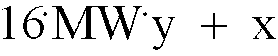

destination space 25, the region outside thedestination space 25 is normalized, and the development is made starting with the heading of thedestination space 25. This applies also in the band buffer structure. - Fig. 6 shows a dot pattern writing address generating circuit in the dot
pattern development section 15. It can access a memory space of 16 Mbytes. - As illustrated, it comprises a
register 30 for storing the heading address RA of the raster buffer 5', aregister 31 for storing the memory capacity (space) RC of the raster buffer 5', registers 32a and 32b for storing destination address for the pointing to a particular bit within thedestination space 25. Aregister 33 stores the number of words, M, per line, i.e., within in the destination memory width MW. These data are set by themicroprocessor 7. - The dot
pattern development section 15 further comprisesadders selectors circuit 44, and wordline border line 45. - The operation of the dot pattern writing address circuit will now be described taking, as an example, the writing of a font pattern at point Q (x, y) in Fig. 5.
- When the heading address RA and the capacity RC of the
destination space 25 are set in theregisters microprocessor 7 via the databus signal lines 18a, the raster buffer 5' is allocated in the memory space in themicroprocessor 7. - When the destination memory width M in terms of the number of words per line is set in the
register 33, and the destination address DA for addressing to a particular bit is set in theregisters pattern development section 15 operates, and the address signal lines and the control signal lines for reading afont pattern 22 from the source memory, e.g., the built-in font memory 4' are enabled. - Then, reading of a
font pattern 22 shown in Fig. 5, with a source data width of L bits, and a source data height of H bits, is started. The reading of thefont pattern 22 is performed a word at a time in the principal scanning direction. When one word of the font pattern that has been read is supplied into the dotpattern development section 15, the source data address signal lines and the control signal lines are disabled, and the one word of the dot pattern that has been supplied are subjected to bit-shifting. The number of bits by which shifting is performed is the deviation of the location where the font is to be allocated from the word boundary in the actual memory. This is because the particular bit of the point Q for developing thefont pattern 22 in thedestination space 25 is pointed. - When the bit shifting is completed, the outputs from the dot pattern writing address circuit of Fig. 6 enable the destination bit address signal lines, data signal lines, not shown, and the control signal lines, and one word of the font pattern having been bit-shifted is developed into the designated location in the
destination space 25, and then the address signal lines, the data signal lines, and the control signal lines are disabled. - The above operations are successively repeated, and when the reading of the L-th bit in the principal scanning direction is completed, the L-th bit reading completion signal is output and after the development of the L-th bit, the operation then proceeds to the reading and development of the next raster , i.e., line, within the font pattern.
- When the above operation is repeated, and the reading and development of the H-th line is completed, the reading of one character of the font pattern is completed, and the operation is terminated.
- Now, the bit shift processing, switching to the next raster and the automatic coupling processing between the last address and the first address of the
destination space 25 will be described. - The output signal of the last (lowest) four bits indicating the bit position (n-1) within the word (16 bits) in the
registers counter 42, and when the contents of the above-mentioned four bits are set in the counter by a counter load signal, not shown, the bit shifting of the font pattern (one word long) that has been supplied to the dotpattern development section 15 and the count-up operation of thecounter 42 are performed synchronously until the carry-out signal of the counter 42 (word-boundary signal 45) is on, i.e., the font pattern data is shifted by (15-(n-1)) bits, and writing with n-bit shifting into thedestination space 25 is now possible. - The font pattern development (writing) in the
destination space 25 will now be described. - The heading address RA for positioning the
destination space 25 in the actual memory is stored in theregister 30, and the memory capacity RC is stored in theregister 31. The heading address RA is set at a location designated by 2n times 64 x K (n = 0, 1, 2 ...), and the memory capacity RC is set to be 2ntime 64 Kbytes (n = 0, 1, 2 ...). Thesignals 46 of the upper 8 bits in the 23 bits are masked with information of thedestination space 25 from theregister 31. For instance, with theregister 31 designating 64 x K (00Hex.) i.e., the space from the address 0 x K to 64 x K, even when thesignals 46 of the upper 8 bits of the destination address are accessing the space of 128 Kbytes (01Hex.), i.e., the space from the address 64 x K to the address 128 x K, the output lines 47 are kept at 00Hex. by the action of the ANDcircuit 44, and the overflow from the 64 x K space is prevented. - In other words, even if development of a font pattern from the 64 x K space (the space from the address 0 x K to the address 64 x K) to the 128 x K space (the space from the address 64 x K to the address 128 x K) occurs, the font pattern that has overflown is automatically stored staring with the head of the 64 x K space (see point Q' (x', y') in Fig. 5).
- The signals on the output lines 47 of the AND
circuit 44 are added, at theadder 34, to the heading address RA of theregister 30, and, using its output signals 48, thedestination space 25 on the actual memory can be accessed. - The address designation and the development in the destination space will now be described.
- The output lines (excepting the lower four bits connected to the counter 42) of the
registers selectors registers - The destination address stored in the
registers counters lines 18b) of thecounters destination space 25 is present is selected, and with the developed data after the above-mentioned n bit shifting, pointing and development (writing) of the designated address are enabled. - When the development of one word is completed, the next word in the principal scanning direction in the
font pattern 22 is read, and the above-mentioned bit shifting is performed, the count values of thecounters destination space 25 is developed. - The
counters font pattern 22 in the principal scanning direction reaches the L-th bit, the L-th bit reading completion signal, not shown, is output from the source memory access circuit, and theselectors adders - At the same time, the outputs of the
register 33 storing the memory width MW in the principal scanning direction of thedestination space 25 and of theregister 40 in which the lower bit information of the destination address (DA) are set are added, and set in theregister 40 via theselector 38. At the same time, the upper bit output information of the destination address (DA) and theregister 39 and the carry signal of theadder 36 and the "0" data are added, and set in theregister 39 via theselector 37. - Input to the
counters registers - When the development of one word is completed, starting with the next word, each time reading and development are performed, the
counters font pattern 22 into thedestination space 25 is thus completed. - Fig. 7 shows a dot pattern reading address circuit.
- As illustrated, it comprises a
register 50 for storing the heading address RA, and aregister 51 for storing the memory capacity of thedestination space 25. Aregister 52 stores a memory width M in terms of the number of words, of thedestination space 25 in the principal scanning direction. The data are set in these registers from themicroprocessor 7 via thedata bus 18a. - The heading address RA can be set at 2n times 64 x K, and the memory capacity RC can be set at 2n
times 64 Kbytes. Thesignals 61 of the upper 8 bits in the 23 bits of the reading address signals to be described later are masked at the ANDcircuit 59 with the information of thedestination space 25. For instance, with theregister 51 designating 64 Kbytes (00Hex.), i.e., a word within the range of from the address 0 x K to the address 64 x K, even when thesignals 61 of the upper 8 bits of the reading address are accessing the space of 128 x K (01Hex.), i.e., the space from the address 64 x K to the address 128 x K, theoutput lines 62 of the ANDcircuit 59 are kept at 00Hex., and does not overflow the 64 x K space. That is, in the event of the reading of a dot pattern exceeding the 64 x K space, there will be automatic switching to the reading which start at the heading dot line in the 64 x K space, and the reading is repeated to complete the reading of the entire information of the page. - The signals on the
output lines 62 of the ANDcircuit 59 are added to the heading address RA from theregister 50 at theadder 60, and itsoutput signals 63 form theaddress 18b for thedestination space 25 on the actual memory, enabling access. - Address designation and reading of the
destination space 25 will now be described. - When the
microprocessor 7 issues a dot pattern reading command, theregisters counters destination space 25. - Subsequently, when the successive MW word reading is performed in the principal scanning direction, responsive to the 1 raster reading signal, not shown, the output information of the
register 54 and the memory width MW information are added at theadder 53, and new information is set in theregister 54. The information in theregister 57, the carry in theadder 53, and the "0" data are added to set new information in theregister 57. - The heading address RA + MW for the next raster newly set are set in the
counters - Fig. 8 shows a raster buffer having three allocations.
- In the auxiliary scanning direction, 1 allocations is comprised of 64 bits, and the
font patterns font pattern 22a is pointed to the point P1 in thewriting allocation 5a' in the raster buffer 5', it is developed in thewriting allocation 5a'. When thefont pattern 22b is pointed to the point P2, its part exceeds thewriting allocation 5a' and the raster buffer 5', and the exceeding part is developed in the write-waitingallocation 5b'. - The reading of the dot pattern of the reading allocation is commenced after development of the
font pattern 22b is completed, and the development of thefont pattern 22b is deferred until the definition of theallocation 5b' is changed to a writing allocation and the definition of theallocation 5c' is changed to a write-waiting allocation. - Figure 9 shows a raster buffer having six allocations.
- In this case, the write-waiting allocation is formed of three allocations (5a1' to 5a3') with the height of 32 dots in the auxiliary scanning direction, the write-waiting allocation is formed of two allocations (5b1' and 5b2') with the height of 32 dots in the auxiliary scanning direction, and the reading allocation is formed of one allocation (5c1') with the height of 32 dots in the auxiliary scanning direction. The total capacity of the six-allocation configuration is identical to that of the three-allocation configuration in Fig. 8.
- When the
font pattern 22a is pointed at the point P1 in the writing allocation 5a1' of the raster buffer 5', it is developed in the writing allocations 5a1' and 5a2'. When thefont pattern 22b is pointed at the point P2 in the writing allocation 5a2', part of thefont pattern 22b is developed in the writing allocation 5a2', and the rest exceeds the raster buffer 5'. The exceeding part of the font pattern is developed in the writing allocation 5a3'. In the above-described three-allocation configuration, when the pointing was made at the point P3, the development of thefont pattern 22c was impossible. In the six-allocation configuration, because of the writing allocation 5a3', it is possible to develop in the writing allocation 5a3' and the write-waiting allocations 5b1' and 5b2'. Moreover, the reading of dot pattern of the reading allocation 5c1' is commenced after the development of thefont pattern 22c is completed. - As has been described, in the case of the six-allocation configuration, reading in the direction of the auxiliary scanning direction, is made for a dot pattern of 32 dots (1 allocation) can be made, as opposed to the three-allocation configuration, margin is provided in the development (writing), so overrun does not occur.
- The invention is not limited to the embodiments described above. Various modifications are possible without departing from the scope of the invention.
- As has been described, the raster buffer for storing dot image data are divided into three allocations in the direction of auxiliary scanning, and the respective allocations are assigned to a writing allocation in which a font font pattern read from a font memory is written, a reading allocation from which dot image data that have been written are read, and a write-waiting allocation in which part of a font pattern that has overflown the writing allocation is written, and the writing allocation and the write-waiting allocation have a capacity for storing a character having the biggest size among those which are used frequently, and prior to printing of dot image data, a font pattern is written in the writing allocation, and the definition of the allocation in which writing has been made is changed to a reading allocation, dot image data is then read from the reading allocation, the definition of the write-waiting allocation waiting for the next writing is changed to a writing allocation, and the definition of the reading allocation from which the reading has been made is changed to a writing allocation, with such change of definition being made successively. As a result, the required memory capacity is reduced, and the cost of the apparatus can be lowered.
- Moreover, when the font pattern exceeds the border at the tail of the raster buffer, the exceeding part is written at the head of the raster buffer, with continuity. As a result, the printing speed can be increased even where complicated patterns or a multiplicity of character patterns are concentrated in a specific area.
Claims (9)
- A printing apparatus comprising a raster buffer (5) for storing character dot image data, reading means (6') for reading dot image data from the buffer, writing means (7) for writing dot image data from a font memory to the buffer, and addressing means (30,..,44;50,..,60) for providing the reading and writing means with concurrent and cyclical access to the buffer, characterized in that the addressing means is configured for addressing the buffer as first, second and third allocations (5a',5b',5c') whose positions within the buffer change cyclically and such that the reading means uses the first allocation and, at the same time, the writing means uses the second allocation, the third allocation providing space for writing dot image data which overflows the second allocation.
- An apparatus according to claim 1, wherein the allocations are the same size.
- An apparatus according to claim 1, wherein the addressing means is configured to address the second allocation as a plurality of sections.
- An apparatus according to claim 3, wherein there are three sections.
- An apparatus according to claim 1, wherein the addressing means is configured to address the third allocation as a plurality of sections.
- An apparatus according to claim 5, wherein there are two sections.
- An apparatus according to any one of claims 3 to 6, wherein the sections are of the same size.
- An apparatus according to any preceding claim, including the font memory (4',14b) programmed with dot image data for a plurality of characters, wherein the writing means is operative to read character dot image data from the font memory and write it to the buffer.
- An apparatus according to any preceding claim, wherein the addressing means comprises size storage means (31) for setting the size of the buffer, position storage means (30) for setting the position of the buffer in the memory space of a microprocessor (7), an address counter (41) for generating addresses in the buffer, and means (34,44) ensuring that write addresses past the end of the buffer are mapped onto addresses at the start of the buffer.
Applications Claiming Priority (2)
| Application Number | Priority Date | Filing Date | Title |
|---|---|---|---|
| JP2130391A JP2740568B2 (en) | 1990-05-22 | 1990-05-22 | Printing equipment |
| JP130391/90 | 1990-05-22 |
Publications (3)
| Publication Number | Publication Date |
|---|---|
| EP0458612A2 EP0458612A2 (en) | 1991-11-27 |
| EP0458612A3 EP0458612A3 (en) | 1992-12-02 |
| EP0458612B1 true EP0458612B1 (en) | 1997-03-05 |
Family
ID=15033196
Family Applications (1)
| Application Number | Title | Priority Date | Filing Date |
|---|---|---|---|
| EP91304624A Expired - Lifetime EP0458612B1 (en) | 1990-05-22 | 1991-05-22 | Printing apparatus |
Country Status (4)
| Country | Link |
|---|---|
| US (1) | US5191430A (en) |
| EP (1) | EP0458612B1 (en) |
| JP (1) | JP2740568B2 (en) |
| DE (1) | DE69124837T2 (en) |
Families Citing this family (13)
| Publication number | Priority date | Publication date | Assignee | Title |
|---|---|---|---|---|
| JP2738863B2 (en) * | 1989-06-16 | 1998-04-08 | キヤノン株式会社 | Image transmission device |
| US5420965A (en) * | 1992-06-05 | 1995-05-30 | Software Projects, Inc. | Single pass method of compressing data transmitted to command driven terminal |
| US5577173A (en) * | 1992-07-10 | 1996-11-19 | Microsoft Corporation | System and method of printer banding |
| JPH06191093A (en) * | 1992-12-25 | 1994-07-12 | Fuji Xerox Co Ltd | Recorder |
| JP3154585B2 (en) * | 1993-03-29 | 2001-04-09 | 富士写真フイルム株式会社 | Line memory controller for printer |
| US5490237A (en) * | 1993-04-26 | 1996-02-06 | Hewlett-Packard Company | Page printer having improved system for receiving and printing raster pixel image data from a host computer |
| JP3347527B2 (en) * | 1994-07-01 | 2002-11-20 | キヤノン株式会社 | Printer and printing method |
| KR970010375B1 (en) * | 1994-10-31 | 1997-06-25 | 삼성전자 주식회사 | Band printing method which protects band overrun error in page printer |
| JP3159113B2 (en) * | 1996-06-19 | 2001-04-23 | セイコーエプソン株式会社 | Image forming method and image forming apparatus |
| US5971518A (en) * | 1997-01-28 | 1999-10-26 | Lexmark International, Inc. | Method of printing with an ink jet printer to inhibit the formation of a print artifact |
| JP4227236B2 (en) * | 1998-02-18 | 2009-02-18 | キヤノン株式会社 | Image processing apparatus, image processing method, and storage medium |
| JP4544669B2 (en) * | 1999-09-30 | 2010-09-15 | 三洋電機株式会社 | Character readout circuit |
| JP6270597B2 (en) * | 2014-04-04 | 2018-01-31 | キヤノン株式会社 | Image forming apparatus |
Family Cites Families (7)
| Publication number | Priority date | Publication date | Assignee | Title |
|---|---|---|---|---|
| JPS59796A (en) * | 1982-06-28 | 1984-01-05 | Yokogawa Hokushin Electric Corp | Dot printer |
| JPS60141076A (en) * | 1983-12-28 | 1985-07-26 | Hitachi Ltd | Control system of printer |
| JPS61129969A (en) * | 1984-11-28 | 1986-06-17 | Toshiba Corp | Printing control device |
| US4694405A (en) * | 1985-07-09 | 1987-09-15 | Office Automation Systems, Inc. | Laser printer controller data alignment device |
| US4805094A (en) * | 1986-08-27 | 1989-02-14 | American Telephone & Telegraph Company | Multi-channel memory access circuit |
| JPS6364474A (en) * | 1986-09-05 | 1988-03-22 | Hitachi Ltd | Image memory control device |
| JPS63292747A (en) * | 1987-05-25 | 1988-11-30 | Hitachi Ltd | Buffer management method |
-
1990
- 1990-05-22 JP JP2130391A patent/JP2740568B2/en not_active Expired - Fee Related
-
1991
- 1991-05-10 US US07/698,384 patent/US5191430A/en not_active Expired - Lifetime
- 1991-05-22 EP EP91304624A patent/EP0458612B1/en not_active Expired - Lifetime
- 1991-05-22 DE DE69124837T patent/DE69124837T2/en not_active Expired - Fee Related
Also Published As
| Publication number | Publication date |
|---|---|
| JP2740568B2 (en) | 1998-04-15 |
| US5191430A (en) | 1993-03-02 |
| EP0458612A3 (en) | 1992-12-02 |
| EP0458612A2 (en) | 1991-11-27 |
| JPH0425478A (en) | 1992-01-29 |
| DE69124837D1 (en) | 1997-04-10 |
| DE69124837T2 (en) | 1997-09-18 |
Similar Documents
| Publication | Publication Date | Title |
|---|---|---|
| US4031519A (en) | Printer | |
| US5104245A (en) | Printing apparatus with form editor | |
| EP0458612B1 (en) | Printing apparatus | |
| EP0180258B1 (en) | Decoder | |
| EP0217448B1 (en) | Raster image processor | |
| JP3337684B2 (en) | Printer control system | |
| EP0357383B1 (en) | Output apparatus | |
| JPS595434B2 (en) | Insatsu Sochi | |
| US5010513A (en) | Data processing apparatus | |
| US5360277A (en) | Label printer with selective memory update | |
| US5237645A (en) | Printing apparatus | |
| EP0217447B1 (en) | Raster image memory | |
| JPS58117036A (en) | Print control device | |
| JP2001096854A (en) | Apparatus and method for printing processing | |
| JPH0483664A (en) | Printer device | |
| JPS6125165B2 (en) | ||
| JPS59221069A (en) | Memory control method | |
| US5781706A (en) | Reducing memory capacity requirements in image output while maintaining output speed | |
| US6577313B1 (en) | Image data control apparatus | |
| JP3193551B2 (en) | Printing equipment | |
| JP2872144B2 (en) | Printing equipment | |
| JPH04323058A (en) | Output method and apparatus | |
| JPH0425479A (en) | Printer | |
| JPH02266965A (en) | Printer | |
| JPH08183208A (en) | Bitmap recording method and recording device |
Legal Events
| Date | Code | Title | Description |
|---|---|---|---|
| PUAI | Public reference made under article 153(3) epc to a published international application that has entered the european phase |
Free format text: ORIGINAL CODE: 0009012 |
|
| AK | Designated contracting states |
Kind code of ref document: A2 Designated state(s): DE FR GB |
|
| PUAL | Search report despatched |
Free format text: ORIGINAL CODE: 0009013 |
|
| AK | Designated contracting states |
Kind code of ref document: A3 Designated state(s): DE FR GB |
|
| 17P | Request for examination filed |
Effective date: 19930224 |
|
| 17Q | First examination report despatched |
Effective date: 19950904 |
|
| GRAG | Despatch of communication of intention to grant |
Free format text: ORIGINAL CODE: EPIDOS AGRA |
|
| GRAH | Despatch of communication of intention to grant a patent |
Free format text: ORIGINAL CODE: EPIDOS IGRA |
|
| GRAH | Despatch of communication of intention to grant a patent |
Free format text: ORIGINAL CODE: EPIDOS IGRA |
|
| GRAA | (expected) grant |
Free format text: ORIGINAL CODE: 0009210 |
|
| AK | Designated contracting states |
Kind code of ref document: B1 Designated state(s): DE FR GB |
|
| ET | Fr: translation filed | ||
| REF | Corresponds to: |
Ref document number: 69124837 Country of ref document: DE Date of ref document: 19970410 |
|
| ET | Fr: translation filed |
Free format text: CORRECTIONS |
|
| PLBE | No opposition filed within time limit |
Free format text: ORIGINAL CODE: 0009261 |
|
| STAA | Information on the status of an ep patent application or granted ep patent |
Free format text: STATUS: NO OPPOSITION FILED WITHIN TIME LIMIT |
|
| 26N | No opposition filed | ||
| REG | Reference to a national code |
Ref country code: GB Ref legal event code: IF02 |
|
| PGFP | Annual fee paid to national office [announced via postgrant information from national office to epo] |
Ref country code: FR Payment date: 20060515 Year of fee payment: 16 |
|
| PGFP | Annual fee paid to national office [announced via postgrant information from national office to epo] |
Ref country code: GB Payment date: 20060517 Year of fee payment: 16 |
|
| PGFP | Annual fee paid to national office [announced via postgrant information from national office to epo] |
Ref country code: DE Payment date: 20060518 Year of fee payment: 16 |
|
| GBPC | Gb: european patent ceased through non-payment of renewal fee |
Effective date: 20070522 |
|
| REG | Reference to a national code |
Ref country code: FR Ref legal event code: ST Effective date: 20080131 |
|
| PG25 | Lapsed in a contracting state [announced via postgrant information from national office to epo] |
Ref country code: DE Free format text: LAPSE BECAUSE OF NON-PAYMENT OF DUE FEES Effective date: 20071201 |
|
| PG25 | Lapsed in a contracting state [announced via postgrant information from national office to epo] |
Ref country code: GB Free format text: LAPSE BECAUSE OF NON-PAYMENT OF DUE FEES Effective date: 20070522 |
|
| PG25 | Lapsed in a contracting state [announced via postgrant information from national office to epo] |
Ref country code: FR Free format text: LAPSE BECAUSE OF NON-PAYMENT OF DUE FEES Effective date: 20070531 |