EP0456212B1 - High frequency common mode choke oder high frequency differential mode choke - Google Patents
High frequency common mode choke oder high frequency differential mode choke Download PDFInfo
- Publication number
- EP0456212B1 EP0456212B1 EP91107485A EP91107485A EP0456212B1 EP 0456212 B1 EP0456212 B1 EP 0456212B1 EP 91107485 A EP91107485 A EP 91107485A EP 91107485 A EP91107485 A EP 91107485A EP 0456212 B1 EP0456212 B1 EP 0456212B1
- Authority
- EP
- European Patent Office
- Prior art keywords
- signal
- choke
- common mode
- conductor
- region
- Prior art date
- Legal status (The legal status is an assumption and is not a legal conclusion. Google has not performed a legal analysis and makes no representation as to the accuracy of the status listed.)
- Expired - Lifetime
Links
Images


Classifications
-
- H—ELECTRICITY
- H01—ELECTRIC ELEMENTS
- H01P—WAVEGUIDES; RESONATORS, LINES, OR OTHER DEVICES OF THE WAVEGUIDE TYPE
- H01P5/00—Coupling devices of the waveguide type
- H01P5/12—Coupling devices having more than two ports
Description
- In the Figures, the first digit of a reference numeral indicates the first figure in which appears the element indicated by that reference numeral.
- This invention relates in general to chokes and differential circuits and relates more particularly to chokes that can operate at high frequencies.
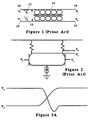
- In circuits having two input ports, the input signal can be divided into the sum of a common mode signal and a differential mode signal. A common mode choke is a circuit that blocks passage of the common mode component of an input signal. A typical existing common mode choke is illustrated in Figure 1. It consists of a pair of
wires ring 13 of ferromagnetic material. Wire ends 14 and 15 serve as a pair of input ports andends input ports ring 13 produces a self inductance L1 inwire 11, a self inductance L2 inwire 12 and a mutual inductance M between these two wires. For a current I1 inwire 11 and I2 inwire 12, the voltages and currents satisfy the relationships:

output ports 

wires ring 13, thereby converting this common mode choke into a differential mode choke. - When
input port 15 of the common mode choke is grounded, the output voltages V3 and V4 onoutput ports output port 17 is grounded, the output voltage V3 is equal to V1 - V2. This version therefore functions as a combiner. - Unfortunately, the choke of Figure 1 does not function effectively at high frequencies. In general, ferrite materials have permeabilities which fall off rapidly at frequencies above several megahertz. At frequencies on the order of 1 GHz or more, the small wavelength (on the order of or less than 4 inches) of the signals becomes comparable in the size to the discrete components of the common mode choke of Figure 1, thereby enabling resonant effects to be important. For such small wavelengths, variations in spacing between windings and other components of that choke can produce resonant effects that result in large variations in operating characteristics, thereby making these devices unsuitable for use at such high frequencies.
- In the JP-A-63/179803 a high frequency power combiner is described which comprises a ground conductor, a first microstrip conductor and a second microstrip conductor, wherein the distance of the microstrip is made narrow for the coupling to supress harmonic waves of a high frequency signal. According to this document high-power signals are combined if those signals are 180° out of phase, whereas signals that are in phase with each other are coupled through a guide path and absorbed by a resistor.
- In the article C. Norman Winningstadt, Nanosecond Pulse Transformers, IRE Trans. Nuclear Science, vol. NS-6, pp. 26-31, March 1959, a transformer is presented that utilizes distributed rather than lumped elements. As discussed in the article Richard E. Matick, Transmission Line Pulse Transformers -- Theory and Applications, Proceedings of the IEEE., Vol. 56, No. 1, January 1968, pp. 47-62, the effects of unwanted "stray inductance and capacitance, if uniformly distributed, can be absorbed into the characteristic impedance of the transmission line, thus avoiding resonant points and providing a broadband device". This articles analyzes the transmission of pulses in short (i.e., comparable in length to a pulse) and long transmission lines above a ground plane and applies this teaching to baluns and transmission line pulse transformers.
- The invention is defined in
claim 1. Advantageous embodiments are specified inclaims 2 to 12. - In accordance with the illustrated preferred embodiment, a choke is presented that is particularly suitable for use at frequencies above 1 GHz. This choke can be connected to function either as a common mode choke or as a differential mode choke. It transmits the low frequency components of the signal substantially undisturbed. This is particularly useful for digital signals in which a low frequency component is needed when a large number of 1's are grouped together in transmission of digital data.
- An important application of this choke is to improve the risetime and overshoot specifications of data pulses produced by a differential output circuit. Most differential output stage designs have excessive overshoot on the falling edge and poor risetime on the rising edge. The common mode choke embodiment can be used to improve the overshoot specification by distributing part of the overshoot of the falling transition to the rising transition. This substantially halves the falling transition overshoot because it is shared by both of these transitions. Similarly, the very fast falling edge is coupled to the slower rising edge, thereby improving the slow risetime at the expense of the fast falltime.
- There are two classes of embodiments of this choke. In a first class, a significant fraction of the unwanted mode signal is reflected back toward the signal source. This choke consists of a transmission line that exhibits a significantly different impedance for a differential mode signal than for a common mode signal. Beads, cores or poly-iron forms can be used to enhance the difference in impedance between the differential and common modes. One or more breaks in one of the transmission line's conductors can be included to substantially increase the impedance of the common mode component. Preferably, such breaks occur in the ground path of the choke so that it can transmit the low frequency components needed for digital data transmission.
- The impedance of one of these modes is selected to match the impedance of input and output transmission lines to which the choke is connected. The mode for which the impedance is equal in both the choke and the transmission lines is transmitted and the mode for which these impedances do not match exhibits partial signal reflection. The fraction of signal reflected is equal to (Z - Z0)/(Z + Z0), where Z is the impedance of the reflected mode and Z0 is the characteristic impedance of the transmission lines. For transmission lines of 50 ohm characteristic impedance Z0, some embodiments exhibit up to a 6:1 ratio of the impedances for the two modes. Embodiments of this choke exist for use with coaxial, microstrip and coplanar transmission lines.
- Unfortunately, such reflected signals can interfere with the operation of devices connected to the input and the output of the choke. For example, when the choke is used at an input port of a test instrument, signals reflected from the input port can interfere with the operation of the device under test and reflections from the output port can interfere with the operation of circuitry within the test instrument. It would therefore be advantageous to absorb the unwanted mode instead of reflecting it A second class of chokes is presented in which the unwanted mode is substantially absorbed instead of reflected.
- Figure 1 illustrates a prior art, low frequency common mode choke.
- Figure 2 illustrates a typical prior art differential mode output device.
- Figure 3A illustrates the overshoot characteristic of the faster of the two transitions of a differential mode pair of signals.
- Figure 3B illustrates the common mode component of the signal of Figure 3A.
- Figure 3C illustrates the differential mode component of the signal of Figure 3A.
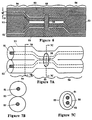
- Figure 4 illustrates a differential output device having improved symmetry between the two signals of this output, having improved transition time for the slower of the two components of this output signal and having reduced overshoot.
- Figure 5 illustrates a microstrip transmission line embodiment of a common mode choke suitable for use at frequencies that include above 1 GHz components.
- Figure 6 illustrates a coplanar transmission line embodiment of a common mode choke suitable for use at frequencies that include above 1 GHz components.
- Figures 7A - 7C illustrate a coaxial transmission line embodiment of a common mode choke suitable for use at frequencies that include above 1 GHz components.
- Figure 8A illustrates, for a differential mode signal, the flow of current in the ground conductor of a coplanar transmission line embodiment of a split-ground type of common mode choke.
- Figure 8B illustrates, for a common mode signal, the flow of current in the ground conductor of a coplanar transmission line embodiment of a split-ground type of common mode choke.
- Figure 9 illustrates a microstrip transmission line embodiment of a split-ground type of common mode choke.
- Figure 10 illustrates a coaxial transmission line embodiment of a split-ground type of common mode choke.
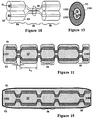
- Figure 11 illustrates a reflection type common mode choke having a plurality of reflection regions to enhance the fraction of an input common mode signal that is reflected.
- Figure 12 is a microstrip transmission line embodiment of an absorption type of common mode choke.
- Figure 13 is a cross-section of a coaxial transmission line embodiment of an absorption type of common mode choke.
- Figure 14 is a coplanar transmission line embodiment of an absorption type of common mode choke.
- Figure 15 illustrates a reflection type common mode choke having a plurality of reflection regions to enhance the fraction of an input common mode signal that is reflected.
- Figure 16 illustrates an alternate coplanar transmission line embodiment of an absorption type of common mode choke.
- In response to transition in a pair of differential mode input signals V1 and V2, the differential transistor pair in the device of Figure 2 exhibits a fast falling transition with overshoot in an output signal V3 and a slower rising transition with no overshoot in an output signal V4 (see Figure 3A). This becomes more noticeable as the amount of current in the differential pair is decreased. The low frequency components of the output pair V3 and V4 are substantially differential mode, but the transitions contain both common mode and differential mode components. That is, V3 and V4 can be represented as Vc + Vd and Vc - Vd, respectively, where Vc and Vd are the common mode component shown in Figure 3B and differential mode components, respectively, shown in Figure 3C.
- The common mode voltage Vc predominantly consists of a high frequency component that is approximately sinusoidal over the interval of a transition and that is zero elsewhere. When V3 and V4 are passed through a high frequency common mode choke that substantially eliminates this high frequency common mode component, the resulting output signals are substantially equal to the differential mode signals Vd and -Vd shown in Figure 3C. These output signals are much more symmetrical, exhibit a reduced rise time on the rising edge and a reduced overshoot on the falling edge. The maximum transition time and overshoot are reduced compared to the pair of signals of Figure 3A. Therefore, the specifications of a differential circuit like that of Figure 2 are improved by passing the output signals V3 and V4 through a high frequency common mode choke. Such a circuit is illustrated in Figure 4, where the output of a
differential output device 41 is coupled through a high frequency common mode choke 42 to provide output signals O1 and O2 in which the high frequency common mode component of the signals V3 and V4 have been substantially eliminated. The resulting signals have lower peak overshoot, faster risetime and greater symmetry. - When an input signal V1 is applied to a
first input port 43 and asecond input port 44 of the common mode choke is grounded, the output voltages V3 and V4 onoutput ports first output port 45 is grounded and input signals V1 and V2 are applied to inputports - A high frequency common mode choke that is useful for digital transmission at greater than 1 GHz clock rates is illustrated in Figure 5. This choke consists of a microstrip conductor transmission line having a pair of
microstrip conductors conductive ground plane 53 by one or more intermediate nonconducting layers 54.Microstrip conductors region 55 than they are in input andoutput regions 56. Inregions 56, the microstrip conductors are separated from one another by a distance D substantially larger than they are spaced fromground plane 53 so that each exhibits a characteristic impedance Z0 determined by the spacing S ofconductors microstrip conductors regions 56. - In
region 55,microstrip conductors microstrip conductors 
microstrip conductors region 54, these currents produce fields that add destructively in most regions thereby producing a smaller total field energy than the field produced by the parallel currents of a common mode signal. - These results are particularly easy to see for the case of two magnetically coupled inductors (i.e., the case n = 2). For this case, equation (5) for the magnetic field energy EH becomes:

- Ideally, this common mode choke transmits substantially all of the differential mode component while reflecting as much of the common mode component as possible. Because there is substantially no interaction within
regions 56 of the signals S1 and S2, the common mode and differential mode components of these two signals will experience the same characteristic impedance Z0. Because spatial variation of the characteristic impedance ofmicrostrip conductors microstrip conductors regions microstrip conductors microstrip conductors - Because the capacitance per unit length between
microstrip conductors region 55 is larger for a common mode signal than for a differential mode signal, within this region the characteristic impedance Z0c for a common mode signal will be larger than for the differential mode signal. This results in the reflection of a fraction (Z0c - Z0)/(Z0c + Z0) of the common mode component without any significant reflection of the differential mode signal. - Because it is advantageous to reflect as much of the common mode signal as possible, the ratio (Z0c - Z0)/(Z0c + Z0) should be as large as possible. This can be improved by the inclusion of ferromagnetic elements within
region 55 to increase the inductive coupling of the common mode component For example, a ferrite ring that encirclesmicrostrip conductors region 55 without changing Z0d within this region or significantly affecting Z0c and Z0d withinregions 56. Z0d is unaffected because the net current throughring 58 is zero for the differential mode current, thereby producing no net change in the circulation of B field withinring 58. However, the net current throughring 58 is nonzero for the common mode component so that the inductance increases for this mode, thereby further increasing Z0c withinregion 55. - Figures 6 and 7A-7C show equivalent embodiments of the common mode choke in coplanar and coaxial transmission line technologies, respectively. The same reference numerals are used in all three embodiments for comparable elements to show the equivalence of all three embodiments. In Figure 6, the
ground conductor 53 is a conductive sheet that is coplanar withsignal conductors conductors conductor 53 is the outer conductor of these two coaxial transmission lines. As illustrated in Figure 7B inregions 56,conductor 53 consists of a pair of cylindrical conductors that are attached at a point of contact. As illustrated in Figure 7C, inregion 55, these two tangent cylindrical shells open at their point of contact to produce a single chamber that encloses bothcenter conductors region 55 compared to the spacing D withinregions 56. As in the embodiment of Figure 5A, aferromagnetic ring 58 can be included that encirclesconductors region 55 to increase further the characteristic impedance Z0c of the common mode component withinregion 55. - Unfortunately, in all three of the above embodiments, it is difficult to get the impedance Z0c substantially above Z0 in
region 55. For such a situation, the fraction of the common mode signal that is reflected is smalL In order to improve the performance when a single discontinuity in the characteristic impedance of the transmission line is small, multiple discontinuities can be used at determined spacing. These multiple discontinuities form an interference filter for the common mode signal. The amount of filtration and frequency band over which the filter operates can be controlled by the spacing and size of the discontinuities. This structure is illustrated in Figure 15 and is also discussed further below in regard to Figure 11. - The following two classes of embodiments can be used to increase the amount of reflected signal from a given discontinuity. In a split-ground class of embodiments, illustrated in Figures 8A and 8B for a coplanar conductor transmission line embodiment, one or
more breaks 81 are introduced intoground conductor 53. As illustrated in Figure 8A, for a differential mode signal, there are complete current paths for the currents inmicrostrip conductors ground conductor sections 53. That is, in the ground conductors, at bothnodes ground plane conductor 53. - At
nodes ground conductor 53. This forces the common mode mirror currents to be carried by ground paths remote frommicrostrip conductors regions 56 on the order of the 300 ohm characteristic impedance for a single wire that is remote from all other conductors. The widths W and separation D of conductors 51 - 53 are varied spatially such that the differential mode impedance Z0d is substantially constant (preferably at 50 ohms). The relative lengths ofregions regions 55 can be arbitrarily short and the lengths of regions can be selected to control interference between the reflected signals from the various discontinuities in the common mode impedance Z0c. Figures 9 and 10 illustrate analogous split-ground embodiments for microstrip and coaxial transmission line embodiments. - The amount of reflected signal can be increased by the inclusion of a multiplicity of
regions 55. This design is illustrated in Figure 11 for a microstrip transmission line, but is clearly applicable to the other types of transmission line embodiments. Because the length of the common mode choke at the high frequencies of interest can be comparable to or longer than the wavelength for such frequencies, interference effects can be significant. In the embodiment of Figure 11,input port 1102 and output port 1103 will generally have a 50 ohm characteristic impedance. The lengths L1 and L2 can be selected to maximize the amount of signal rejection at a selected frequency f0, such as at the frequency of the fundamental sinusoidal component of the sine-like signal between points A and B in Figure 3B. Other embodiments are also possible that have peak common mode rejection at a set of n design frequencies f1, ... , f2. This can be achieved by varying the lengths, conductor widths and conductor spacings of the sections of the choke. Such analysis is well known from standard interference theory. - There are applications in which the signals reflected from the input and output ports of the choke will interfere with the operation of devices coupled to those ports. If the input and output loads coupled to the input and output port of any of the above embodiments is not exactly 50 ohms, then multiple reflections can result. Because one of these loads is often part of a device under test, the value of this load is not controlled by the manufacturer of the above embodiments so that such load will often not be 50 ohms. In such applications, it is advantageous to absorb the common mode signal instead of reflecting it.
- Figure 12 illustrates a microstrip transmission line embodiment of a choke in which the common mode component of an input signal is absorbed. This embodiment differs from the embodiment of Figure 5 by the addition of a
rectangular hole 1201 in the ground plane. Within this hole are one or moreconductive islands 1202, each of which is centered laterally undermicrostrips region 55 and insulated from these microstrips by the substrate. Each ofconductive islands 1202 is connected to groundplane 53 by a pair ofresistors 1203.Resistors 1203 can be arbitrarily adjusted to tailor loss characteristics. For a differential mode signal, each island remains at ground potential so that no power is dissipated through these resistors. However, for a common mode signal, the potential of each island will vary away from ground potential, thereby producing a dissipative flow of current from the islands to the ground plane. When there are a plurality of islands, the gap between adjacent islands should be small enough that it does not introduce a significant discontinuity into the characteristic impedances Z0c and Z0d inregion 55. Each island should be much shorter than a half wave of the highest frequency of operation to avoid undesirable resonances. - A transmission line embodiment of this common mode absorptive-type choke is substantially like that in Figure 7A except that, in
region 55, the cross-section is as shown in Figure 13 instead of as in Figure 7C. Figure 13 illustrates that, withinregion 55, this choke includes anonconductive spacer 1201 that is encircled by aconductive cylinder 1202 and aresistive spacer 1203. As in the embodiment of Figure 12, when a common mode signal passes alongcenter conductors ring 1202 will vary away from ground, thereby producing a dissipative current throughresistor 1203 toouter conductor 53. - Figure 14 illustrates an absorptive-type common mode choke for use with coplanar transmission lines. A pair of
resistive strips 1203 are connected to each ofconductors 53, 53' and 53'' so that a common mode signal produces currents within these resistive strips that damp the common mode signal. Insulating layers 1402 prevent these resistive strips from making electrical contact withconductive lines - Figure 16 illustrates an alternate embodiment of an absorptive-type common mode choke for use with coplanar transmission lines. Analogous to the choke of Figure 12,
resistive elements 1203 are included to dissipate the common mode component. An insulatinglayer 1401 preventsresistive elements 1203 from making electrical contact withconductors conductors Conductors 53 provide the functionality ofislands 1202 in Figure 12. - It should be noted that, although in all of the embodiments, the spacing S between
conductors output regions 56 than inintermediate region 55, the opposite could be the case in the embodiments of Figures 5, 6, and 7A - 7C. In such a case, the ferromagnetic element would still be located in the region where the spacing S is smaller. In this case, such region would beregion 56. These alternate embodiments would still be designed such that the characteristic impedance Z0d within the input andoutput regions 56 matches the characteristic impedance Z0d of transmission lines to which this choke is to be coupled. - These common mode chokes can also be connected to operate as differential mode chokes. For example, in the common mode choke of Figure 5, a pair of
ports ports ports ports
Claims (12)
- A choke comprising:a ground conductor (53);a first signal conductor (51) adjacent the ground conductor and defining therewith a transmission line having a first input port and a first output port; anda second signal conductor (52) adjacent the ground conductor and defining therewith a transmission line having a second input port and a second output port,the first and second signal conductors defining signal paths that have a characteristic common mode impedance and a characteristic differential mode impedance,the second signal conductor being spaced apart from the first signal conductor in a first region (55) by a distance that causes coupling of the two signal paths and characterised in that said distance causes the common mode and differential mode impedances to be unequal to each other in the first region, further characterised in that the choke functions either as a common or as a differential mode choke i.e. one of the modes in the output signals is alternated relative to the other mode.
- A choke as in claim 1 wherein the second signal conductor (52) is spaced apart from the first signal conductor (51) in a second region (56) by a distance that causes the common mode and differential mode impedances to be substantially equal to each other in the second region.
- A choke as in claim 2 wherein the second signal conductor (52) is spaced apart from the first signal conductor (51) in a third region (56) by a distance that causes the common mode and differential mode impedances to be substantially equal to each other in the third region.
- A choke as in claim 2 or claim 3 wherein the differential mode impedance in the first region (55) is substantially equal to the differential mode impedance in the second region (56).
- A choke as in any preceding claim and further comprising an annular ferromagnetic material (58) around the signal conductors (51, 52) in the first region (55).
- A choke as in any preceding claim wherein the signal conductors (51, 52) comprise microstrip transmission lines and the ground conductor (53) comprises a ground plane.
- A choke as in any of claims 1 to 5 wherein the ground conductor (53) surrounds the signal conductors (51, 52) coaxially.
- A choke as in any preceding claim wherein the ground conductor (53) includes a nonconducting region (81) that prevents any common mode signal from flowing in the ground conductor.
- A choke as in any preceding claim and further comprising a plurality of regions (55, 56) in alternate ones (55) of which the second signal conductor (52) is spaced apart from the first conductor (51) by a distance that causes the common mode and differential mode impedances to be unequal to each other and in alternate ones (56) of which the second signal conductor is spaced apart from the first signal conductor by a distance that causes the common mode and differential mode impedances to be substantially equal to each other.
- A choke as in any preceding claim and further comprising means (1201-1203) adjacent the signal conductors (51, 52) for absorbing a common mode signal.
- A choke as in claim 10 wherein the means for absorbing a signal comprises:a conductive island (1202) located in an opening (1201) defined in the ground conductor (53', 53") adjacent the signal conductors (51, 52), the conductive island having an electric potential that is unaltered by a differential mode signal between the signal conductors and that is altered by a common mode signal between the signal conductors; anda resistive element (1203) connecting the island and the ground conductor.
- Use of a choke as claimed in any preceding claim in a differential output device wherein the differential mode impedance of the Choke is selected to substantially match the impedance of a transmission line connected to an input port of the differential output device.
Applications Claiming Priority (2)
| Application Number | Priority Date | Filing Date | Title |
|---|---|---|---|
| US522287 | 1990-05-11 | ||
| US07/522,287 US5138287A (en) | 1990-05-11 | 1990-05-11 | High frequency common mode choke |
Publications (3)
| Publication Number | Publication Date |
|---|---|
| EP0456212A2 EP0456212A2 (en) | 1991-11-13 |
| EP0456212A3 EP0456212A3 (en) | 1992-10-07 |
| EP0456212B1 true EP0456212B1 (en) | 1996-10-30 |
Family
ID=24080261
Family Applications (1)
| Application Number | Title | Priority Date | Filing Date |
|---|---|---|---|
| EP91107485A Expired - Lifetime EP0456212B1 (en) | 1990-05-11 | 1991-05-08 | High frequency common mode choke oder high frequency differential mode choke |
Country Status (4)
| Country | Link |
|---|---|
| US (1) | US5138287A (en) |
| EP (1) | EP0456212B1 (en) |
| JP (1) | JPH04230102A (en) |
| DE (1) | DE69122903T2 (en) |
Families Citing this family (26)
| Publication number | Priority date | Publication date | Assignee | Title |
|---|---|---|---|---|
| US5243308A (en) * | 1992-04-03 | 1993-09-07 | Digital Equipment Corporation | Combined differential-mode and common-mode noise filter |
| JPH07263923A (en) * | 1994-03-23 | 1995-10-13 | Murata Mfg Co Ltd | 90× distributor |
| US6016086A (en) * | 1998-04-03 | 2000-01-18 | Nortel Networks Corporation | Noise cancellation modification to non-contact bus |
| US6677831B1 (en) * | 2001-01-31 | 2004-01-13 | 3Pardata, Inc. | Differential impedance control on printed circuit |
| US6765450B2 (en) | 2002-06-28 | 2004-07-20 | Texas Instruments Incorporated | Common mode rejection in differential pairs using slotted ground planes |
| JP2004129053A (en) * | 2002-10-04 | 2004-04-22 | Mitsubishi Electric Corp | Dc blocking circuit and communication equipment |
| US6956444B2 (en) * | 2003-02-14 | 2005-10-18 | Intel Corporation | Method and apparatus for rejecting common mode signals on a printed circuit board and method for making same |
| US7013437B2 (en) * | 2003-06-25 | 2006-03-14 | Broadcom Corporation | High data rate differential signal line design for uniform characteristic impedance for high performance integrated circuit packages |
| US7430291B2 (en) * | 2003-09-03 | 2008-09-30 | Thunder Creative Technologies, Inc. | Common mode transmission line termination |
| DE10342611A1 (en) * | 2003-09-12 | 2005-04-14 | Hüttinger Elektronik Gmbh + Co. Kg | 90 ° hybrid for splitting or merging high-frequency power |
| EP1699107B1 (en) | 2005-03-05 | 2017-05-31 | TRUMPF Hüttinger GmbH + Co. KG | 3 dB coupler |
| ATE344973T1 (en) | 2005-03-10 | 2006-11-15 | Huettinger Elektronik Gmbh | VACUUM PLASMA GENERATOR |
| JP2006332302A (en) * | 2005-05-26 | 2006-12-07 | Murata Mfg Co Ltd | Common mode choke coil mounted substrate and common mode choke coil mounting method |
| US8384493B2 (en) * | 2006-07-06 | 2013-02-26 | The Ohio State University Research Foundation | Emulation of anisotropic media in transmission line |
| ES2321792B1 (en) * | 2007-10-03 | 2010-03-04 | Diseño De Sistemas En Silicio S.A. | MULTIINJECTION VOLTAGE DEVICE ON MULTIPLE DRIVERS. |
| DE102011113656A1 (en) * | 2011-09-19 | 2013-03-21 | Erni Electronics Gmbh | Multi-layer electrical circuit board |
| EP2597481A1 (en) * | 2011-11-22 | 2013-05-29 | Koninklijke Philips Electronics N.V. | RF-safe interventional or non-interventional instrument for use in an MRI apparatus |
| CN102694226A (en) * | 2012-05-31 | 2012-09-26 | 安徽海特微波通信有限公司 | Weak-coupling directional coupler |
| US20150173256A1 (en) * | 2013-12-17 | 2015-06-18 | Lenovo Enterprise Solutions (Singapore) Pte. Ltd. | Emi suppression technique using a transmission line grating |
| JP6107672B2 (en) * | 2014-01-06 | 2017-04-05 | 日立金属株式会社 | Cable with connector |
| US9484609B2 (en) | 2014-03-04 | 2016-11-01 | Raytheon Company | Microwave coupling structure for suppressing common mode signals while passing differential mode signals between a pair of coplanar waveguide (CPW) transmission lines |
| US9647310B2 (en) * | 2014-03-04 | 2017-05-09 | Raytheon Company | Coplanar waveguide transmission line structure configured into non-linear paths to define inductors which inhibit unwanted signals and pass desired signals |
| US10153238B2 (en) * | 2014-08-20 | 2018-12-11 | Samsung Display Co., Ltd. | Electrical channel including pattern voids |
| CN106550531A (en) * | 2015-09-17 | 2017-03-29 | 鸿富锦精密工业(武汉)有限公司 | Circuit board |
| CN110277619B (en) * | 2019-06-18 | 2024-01-19 | 深圳振华富电子有限公司 | Balun transformer |
| CN115980451B (en) * | 2022-12-05 | 2023-06-23 | 哈尔滨理工大学 | Extraction method of alternating-current equivalent resistance of large-section cable conductor |
Family Cites Families (11)
| Publication number | Priority date | Publication date | Assignee | Title |
|---|---|---|---|---|
| US3659228A (en) * | 1970-07-30 | 1972-04-25 | Rca Corp | Strip-type directional coupler having elongated aperture in ground plane opposite coupling region |
| US3778759A (en) * | 1971-12-27 | 1973-12-11 | Texas Instruments Inc | Static filter for long line data systems |
| US3827001A (en) * | 1973-06-25 | 1974-07-30 | Us Navy | Wide band series-connected equal amplitude power divider |
| US3979699A (en) * | 1974-12-23 | 1976-09-07 | International Business Machines Corporation | Directional coupler cascading for signal enhancement |
| US4121180A (en) * | 1976-12-27 | 1978-10-17 | Technical Research And Manufacturing, Inc. | Broadband directional coupler |
| US4222016A (en) * | 1977-10-05 | 1980-09-09 | Endress U. Hauser Gmbh U. Co. | High frequency transformer |
| US4591812A (en) * | 1982-11-22 | 1986-05-27 | Communications Satellite Corporation | Coplanar waveguide quadrature hybrid having symmetrical coupling conductors for eliminating spurious modes |
| JPS6041815A (en) * | 1983-08-17 | 1985-03-05 | Matsushita Electric Ind Co Ltd | Pulse circuit |
| US4800344A (en) * | 1985-03-21 | 1989-01-24 | And Yet, Inc. | Balun |
| JPH0229003A (en) * | 1988-07-18 | 1990-01-31 | Nippon Telegr & Teleph Corp <Ntt> | High frequency power combiner and distributor |
| US4980654A (en) * | 1990-04-06 | 1990-12-25 | Tektronix, Inc. | Transmission line transformer |
-
1990
- 1990-05-11 US US07/522,287 patent/US5138287A/en not_active Expired - Lifetime
-
1991
- 1991-05-08 DE DE69122903T patent/DE69122903T2/en not_active Expired - Fee Related
- 1991-05-08 EP EP91107485A patent/EP0456212B1/en not_active Expired - Lifetime
- 1991-05-10 JP JP3135615A patent/JPH04230102A/en active Pending
Also Published As
| Publication number | Publication date |
|---|---|
| EP0456212A3 (en) | 1992-10-07 |
| DE69122903D1 (en) | 1996-12-05 |
| EP0456212A2 (en) | 1991-11-13 |
| US5138287A (en) | 1992-08-11 |
| JPH04230102A (en) | 1992-08-19 |
| DE69122903T2 (en) | 1997-05-28 |
Similar Documents
| Publication | Publication Date | Title |
|---|---|---|
| EP0456212B1 (en) | High frequency common mode choke oder high frequency differential mode choke | |
| US3999150A (en) | Miniaturized strip-line directional coupler package having spirally wound coupling lines | |
| Magnusson et al. | Transmission lines and wave propagation | |
| US4012703A (en) | Transmission line pulse transformers | |
| US2751558A (en) | Radio frequency filter | |
| JPS5943103B2 (en) | Josefson device array | |
| US3037175A (en) | Broadband transformers | |
| US9300028B2 (en) | Frequency selective limiter | |
| US5808518A (en) | Printed guanella 1:4 balun | |
| US5153171A (en) | Superconducting variable phase shifter using squid's to effect phase shift | |
| US3735267A (en) | Balanced mixer | |
| US3016495A (en) | Magnetostatic microwave devices | |
| CN113659300A (en) | Broadband four-power divider | |
| US3521198A (en) | Electronically controlled delay line | |
| US6756874B2 (en) | Series transmission line transformer | |
| US4525689A (en) | N×m stripline switch | |
| USH432H (en) | Slot line tunable bandpass filter | |
| US3480884A (en) | Electromagnetic wave energy coupling apparatus comprising an anisotropic dielectric slab | |
| US5281932A (en) | Multilayer magnetically coupled suspended stripline for impedance matching | |
| US3529233A (en) | Lattice type phase shifting network | |
| US6833754B2 (en) | Radio frequency filter | |
| Dunn et al. | New design techniques for miniature VHF circulators | |
| US3092782A (en) | Solid state traveling wave parametric amplifier | |
| US3539953A (en) | Magnetically tunable comb line bandpass filter | |
| US5923227A (en) | Non-linear dispersive transmission line |
Legal Events
| Date | Code | Title | Description |
|---|---|---|---|
| PUAI | Public reference made under article 153(3) epc to a published international application that has entered the european phase |
Free format text: ORIGINAL CODE: 0009012 |
|
| AK | Designated contracting states |
Kind code of ref document: A2 Designated state(s): DE GB |
|
| PUAL | Search report despatched |
Free format text: ORIGINAL CODE: 0009013 |
|
| AK | Designated contracting states |
Kind code of ref document: A3 Designated state(s): DE GB |
|
| 17P | Request for examination filed |
Effective date: 19930217 |
|
| 17Q | First examination report despatched |
Effective date: 19941222 |
|
| GRAG | Despatch of communication of intention to grant |
Free format text: ORIGINAL CODE: EPIDOS AGRA |
|
| GRAH | Despatch of communication of intention to grant a patent |
Free format text: ORIGINAL CODE: EPIDOS IGRA |
|
| GRAH | Despatch of communication of intention to grant a patent |
Free format text: ORIGINAL CODE: EPIDOS IGRA |
|
| GRAA | (expected) grant |
Free format text: ORIGINAL CODE: 0009210 |
|
| AK | Designated contracting states |
Kind code of ref document: B1 Designated state(s): DE GB |
|
| REF | Corresponds to: |
Ref document number: 69122903 Country of ref document: DE Date of ref document: 19961205 |
|
| PLBE | No opposition filed within time limit |
Free format text: ORIGINAL CODE: 0009261 |
|
| STAA | Information on the status of an ep patent application or granted ep patent |
Free format text: STATUS: NO OPPOSITION FILED WITHIN TIME LIMIT |
|
| 26N | No opposition filed | ||
| REG | Reference to a national code |
Ref country code: GB Ref legal event code: IF02 |
|
| PGFP | Annual fee paid to national office [announced via postgrant information from national office to epo] |
Ref country code: GB Payment date: 20040505 Year of fee payment: 14 |
|
| PGFP | Annual fee paid to national office [announced via postgrant information from national office to epo] |
Ref country code: DE Payment date: 20040630 Year of fee payment: 14 |
|
| PG25 | Lapsed in a contracting state [announced via postgrant information from national office to epo] |
Ref country code: GB Free format text: LAPSE BECAUSE OF NON-PAYMENT OF DUE FEES Effective date: 20050508 |
|
| PG25 | Lapsed in a contracting state [announced via postgrant information from national office to epo] |
Ref country code: DE Free format text: LAPSE BECAUSE OF NON-PAYMENT OF DUE FEES Effective date: 20051201 |
|
| GBPC | Gb: european patent ceased through non-payment of renewal fee |
Effective date: 20050508 |