EP0455493A2 - Tapered notch antenna - Google Patents
Tapered notch antenna Download PDFInfo
- Publication number
- EP0455493A2 EP0455493A2 EP91303990A EP91303990A EP0455493A2 EP 0455493 A2 EP0455493 A2 EP 0455493A2 EP 91303990 A EP91303990 A EP 91303990A EP 91303990 A EP91303990 A EP 91303990A EP 0455493 A2 EP0455493 A2 EP 0455493A2
- Authority
- EP
- European Patent Office
- Prior art keywords
- notch
- antenna
- tapered
- region
- feed
- Prior art date
- Legal status (The legal status is an assumption and is not a legal conclusion. Google has not performed a legal analysis and makes no representation as to the accuracy of the status listed.)
- Withdrawn
Links
Images

Classifications
-
- H—ELECTRICITY
- H01—ELECTRIC ELEMENTS
- H01Q—ANTENNAS, i.e. RADIO AERIALS
- H01Q13/00—Waveguide horns or mouths; Slot antennas; Leaky-waveguide antennas; Equivalent structures causing radiation along the transmission path of a guided wave
- H01Q13/08—Radiating ends of two-conductor microwave transmission lines, e.g. of coaxial lines, of microstrip lines
- H01Q13/085—Slot-line radiating ends
Definitions
- This application relates to notch/slotline antennas.
- the present invention pertains to linearly polarized notch (i. e., slotline) antennas that are tapered outward toward the open end.
- notch i. e., slotline
- an open-ended slot or notch radiator is a relatively broadband element especially when flared as a broadband transition to free space. It has important advantages which are desirable, such as being light in weight, cheaply manufactured with printed circuit board techniques that are capable of accurate replication from unit to unit.
- Tapered notch antennas excited by a microstrip feedline are known in the art.
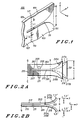
- Such a prior art antenna is shown in Fig. 1.
- a planar surface 101 such as a circuit board with a front side 103 and a back side 105.
- the front side 103 has a metallized surface 107 with a tapered notched area 111 etched away to expose a dielectric substrate 109. This area extends to the edge finalized as dimension A.
- the back side 105 comprises the dielectric substrate 109 with a metallized strip 113 affixed thereon.
- the metallized surface 107 forms a ground plane for the microstrip feed line 113.
- the signal to be transmitted is applied to the strip 113 and coupled to the tapered notch 111 by means of the cross-over junction 115.
- the length L1 of the open circuit stub 117 of the strip 113, and the length L2 of the short circuited stub of the notch 111 are adjusted for optimum coupling at the junction 115.
- a notch antenna begins to radiate when the width of the notch as manifested by the taper becomes excessively wide. It is known that if the guide wavelength in the notch exceeds about 0.4 free space wavelength, then radiation results.
- the radiation may be controlled by the taper as a travelling wave outward toward the flared open end A.
- the dielectric helps confine the fields to within the region of the notch.
- the radiation pattern in the E-plane has maximum directivity in the direction of P determined, in part, by the electrical dimension of A.
- the H-plane radiation pattern has a very broad cardioid shape with a deep null in the direction of the shorted end of the notch and the maximum at the taper end in the direction of P.
- a stripline feed is used to implement a simple double conductive plane divergent tapered notch to yield twin phase centers useful for the increase of H-plane directivity.
- a feed line structure is utilized that is a coplanar line, meaning that all conductors of the transmission line and the notch are in the same plane.
- this embodiment requires access to only one side of the printed circuit board for fabrication. This structure lends itself to simpler fabrication and to array techniques for increasing the H-plane directivity.
- the directivity of the H-plane pattern directivity is increased by splitting the tapered region of the second embodiment into two or more conducting surfaces.
- the surfaces each contain the original tapered configuration and diverge outward away from one another in a controlled fashion, thereby forming an array in the H-plane of multiple phase centers of radiation. Due to the controlled divergence, the array has at the taper end of each diverging surface a controlled amplitude and phase, which combined yields an H-plane pattern shape and directivity beyond that of the single plane (single phase center) tapered notch element.
- a single split, two surface, equal-taper element will have similarities to a twin dipole array of equivalent H-plane spacing.
- the invention provides an antenna comprising: a planar surface with metal coating disposed thereon, the metal coating removed in a first essentially linear region to form a stripline feed, the metal coating removed in a second region to form a notch having a closed narrow end and a relatively wider end that is open; said stripline feed region intersecting said notch at a coplanar junction located near said narrow end of said stripline feed, the notch forming two metallic fingers that extend away from said coplanar junction and toward the open wider end; wherein each of said two metallic fingers is split into two leaves, the leaves parted and separated relative to each other; and, wherein said leaves diverge outward from one another toward said open wider end.
- the invention provides an antenna comprising: an essentially planar dielectric surface having an edge with a metal coating disposed thereon, the metal coating removed in a first essentially linear region to form a coplanar waveguide feed, the metal coating removed in a second region to form a notch having a closed narrow end and a tapered wider end that is open at the edge of the dielectric surface, the coplanar waveguide feed intersecting the notch at a coplanar junction located near the closed narrow end of the notch.
- the invention provides an antenna comprising: a feed line and a notch radiator, said notch radiator having a closed narrow end, the other end having a wider tapered region that is open, said feed line and said notch radiator being coplanar, with the feed line and the notch radiator conductors in the same plane and disposed on a dielectric surface, said feed line coupled to said notch radiator by means of a coplanar junction located near the closed narrow end of the notch.
- the invention provides an antenna comprising: two thin dielectric substrates, the first substrate having an outer side and an inner side, the outer side having a metallic surface disposed thereon, the inner side having a metallized strip affixed thereon whose function is that of a stripline, the second substrate having an outer side and an inner side, the outer side having a metallic surface disposed thereon, the inner side unmetallized, the metallized surfaces both having substantially identical portions of the metallic coating removed by etching to form a tapered notch on each surface, each notch having a narrow closed end and a relatively wider tapered end that is open, the inner surfaces of both substrates bonded together in the region near the narrow closed end of the notch, the inner surfaces of both substrates separated from each other in the region near the wider tapered end of the notch, the inner surfaces diverging outward one from another towards the open end of the notch.
- the invention provides a printed circuit board including an antenna, the antenna comprising: an essentially planar metallic surface, the metal coating removed in a first essentially linear region to form a coplanar waveguide feed, the metal coating removed in a second region to form a notch having a closed narrow end and a tapered wider end that is open at the edge of the dielectric surface, the coplanar waveguide feed intersecting the notch at a coplanar junction located near the closed narrow end of the notch.
- the invention provides a printed circuit board including an antenna, the printed circuit board including a surface, the antenna comprising: a feed line comprising a first area of the printed circuit board surface having conductive metal deposited thereon and a notch radiator comprising a second area of the printed circuit board surface having conductive metal deposited thereon, said notch radiator having a closed narrow end, the other end having a wider tapered region that is open, the feed line being generally elongated and having a relatively narrow width; the notch radiator and the feed line each running in a generally orthogonal direction to each other; said feed line coupled to said notch radiator by means of a coplanar junction located near the closed narrow end of the notch.
- the invention provides an antenna comprising: two thin dielectric substrates, the first substrate having an outer side and an inner side, the outer side unmetallized, the inner side having a metallic surface disposed thereon, the inner side metallic coating of said first substrate removed to form a tapered notch with coplanar transmission line feed, said notch radiator having a narrow closed end and a relatively wider tapered end that is open and said coplanar transmission line feed located in the region of said narrow end, the second substrate having an outer side and an inner side, the outer side unmetallized and the inner side having a metallic surface disposed thereon, the metallic coating of said second substrate removed in substantially identical portions as that of the first substrate but in mirror image such that when the inner surfaces are placed together an alignment of the metallic coating is achieved, the inner surfaces of both substrates bonded together in the region near the narrow closed end of the notch, the inner surfaces of both substrates separated from each other in the region near the wider tapered end of the notch.
- Fig. 1 shows a microstrip feed antenna, as in the prior art.
- Fig. 2A-2B show a first embodiment of a tapered notch antenna, according to the invention.
- Fig. 3 shows a second embodiment of a tapered notch antenna, according to the invention.
- Fig. 4A-4B show a third embodiment of a tapered notch antenna, according to the invention.
- Fig. 2A there is shown a side view of a first embodiment of a tapered notch antenna, according to the invention.
- an antenna that is formed by using a conventional stripline printed circuit board technique consisting of two thin dielectric substrates 219 and 221.
- the side 201 of substrate 219 has a metallic coating 215 disposed thereon.
- the other (inner) side of substrate 219 has a metallized strip 211 affixed thereon whose function is that of a conductive stripline track.
- a metallic coating 217 is disposed thereon.
- the other (inner) side of substrate 221 is unmetallized.
- the metallized surfaces 215 and 217 of substrates 219 and 221 respectively have identical portions of the metallic coating removed by etching to form a tapered notch depicted by 213 on the outer surfaces of both substrates, thus exposing the dielectric substrates 219 and 221.
- the outer metallized surfaces 215 and 217 form the ground planes for the stripline feed whose conductive track is metallized strip 211 on the inner surface of substrate 219.
- the spacing B gives an amay factor to the H-plane directivity and is adjustable, thus enabling the width of the cardioid shape to be reduced.
- Maximum directivity of the array is in the direction of P, and the E and H field components are as indicated in Fig. 2B.
- a second embodiment of a tapered notch antenna there is shown a planar dielectric surface 305 with a metallic coating 301 disposed thereon.
- the metallic coating has a portion removed by etching forming a tapered notch portion 307, notch portion 311 and a coplanar waveguide portion 309.
- a signal to be transmitted is applied to the coplanar waveguide between the center metallic strip 317 and the metallic coating 301.
- the coplanar waveguide field excitation is TEM in nature.
- the coplanar waveguide forms a cross junction 319. Shorted stub 313 of the coplanar waveguide extends beyond the notch and forms a reactance at the junction 319.
- the shorted stub 315 of the notch also forms a reactance at the junction 319, and can be adjusted to provide optimum field coupling one to the other, coplanar waveguide to notch.
- the taper 307 provides an impedance transition from the slotline to the board edge aperture A where the travelling wave couples to space and radiation results outward normal to the edge in the direction of propagation P.
- the plane containing the notch is thus the E-plane, and the E and H field vectors are as labeled in Fig. 3.
- the radiation pattern in the E-plane has a maximum directivity in the direction of P determined, in part, by the electrical dimension of A.
- the H-plane radiation pattern has a broad cardioid shape with the null in the direction of the shorted end of the notch and the maximum at the taper end in the direction of P. Reciprocity holds for the embodiment.
- Fig. 4A there is shown a side view of a third embodiment of a tapered notch antenna, according to the invention.
- the antenna element is formed of a thin metal plane 411 with thin dielectric substrates 417 and 419 on each side.
- the dielectric substrate boundaries are omitted for clarity in Fig. 4A.
- the metal plate 411 is split into two identical planes 413 and 415 each with its dielectric substrate 417 or 419 at the line X-X.
- the notch area 409 diverges into two separate identical notches and tapered planes 413 and 415 with attendant dielectric substrates 417 and 419.
- the tapered plane 415 depicted as being farthest away from the viewer comprises an upper portion 415A with a tip designated Z and a lower portion 415B with a tip designated Z′.
- Fig. 4B there is shown a top view of the second embodiment, indicating the boundaries of the dielectric substrates 417 and 419.
- the metal plane 411 splits at the line X to become two curved planes 413 and 415, separated by a distance B at their tips.
- the feed 407 is a coplanar wave guide with cross junction to the notch 409 matched by reactive stubs 405 and 403.
- the split of the notch 409 into two tapered planes 413 and 415 results in discrete apertures Y-Y′ and Z-Z′ similar to two dipoles, one oriented along the line Y-Y′ and the other along the line Z-Z′.
- these apertures Y-Y′ and Z-Z′ represent a two-element array of inphase elements spaced apart by a distance B. This spacing gives H-plane pattern directivity control and may be adjusted as desired.
Abstract
Description
- This application relates to notch/slotline antennas.
- The present invention pertains to linearly polarized notch (i. e., slotline) antennas that are tapered outward toward the open end. As is known, an open-ended slot or notch radiator is a relatively broadband element especially when flared as a broadband transition to free space. It has important advantages which are desirable, such as being light in weight, cheaply manufactured with printed circuit board techniques that are capable of accurate replication from unit to unit.
- Tapered notch antennas excited by a microstrip feedline are known in the art. Such a prior art antenna is shown in Fig. 1. There is shown a
planar surface 101 such as a circuit board with afront side 103 and aback side 105. Thefront side 103 has ametallized surface 107 with a taperednotched area 111 etched away to expose adielectric substrate 109. This area extends to the edge finalized as dimension A. Theback side 105 comprises thedielectric substrate 109 with ametallized strip 113 affixed thereon. Themetallized surface 107 forms a ground plane for themicrostrip feed line 113. - As is known, the signal to be transmitted is applied to the
strip 113 and coupled to thetapered notch 111 by means of the cross-over junction 115. The length L₁ of theopen circuit stub 117 of thestrip 113, and the length L₂ of the short circuited stub of thenotch 111 are adjusted for optimum coupling at the junction 115. A notch antenna begins to radiate when the width of the notch as manifested by the taper becomes excessively wide. It is known that if the guide wavelength in the notch exceeds about 0.4 free space wavelength, then radiation results. The radiation may be controlled by the taper as a travelling wave outward toward the flared open end A. The dielectric helps confine the fields to within the region of the notch. At that point, nearly matched impedance conditions exist and launch of the field occurs with the E- and H-field components and the maximum radiation direction P as indicated. The wave polarization is parallel with the plane of the notch and the attendant taper. A phase center exists essentially at the center of the end of the flare A, and reciprocity holds for the system. - The radiation pattern in the E-plane has maximum directivity in the direction of P determined, in part, by the electrical dimension of A. The H-plane radiation pattern has a very broad cardioid shape with a deep null in the direction of the shorted end of the notch and the maximum at the taper end in the direction of P.
- One problem with the prior art arrangement, as in Fig. 1, is that it has low directivity in the H-plane. It is desirable, therefore, to provide an improved tapered notch antenna.
-
- It is an object of the invention to provide an improved tapered notch antenna.
- Therefore, an improved tapered notch antenna is provided. In a first embodiment, a stripline feed is used to implement a simple double conductive plane divergent tapered notch to yield twin phase centers useful for the increase of H-plane directivity.
- In a second embodiment, a feed line structure is utilized that is a coplanar line, meaning that all conductors of the transmission line and the notch are in the same plane. As a result, this embodiment requires access to only one side of the printed circuit board for fabrication. This structure lends itself to simpler fabrication and to array techniques for increasing the H-plane directivity.
- In a third embodiment, the directivity of the H-plane pattern directivity is increased by splitting the tapered region of the second embodiment into two or more conducting surfaces. The surfaces each contain the original tapered configuration and diverge outward away from one another in a controlled fashion, thereby forming an array in the H-plane of multiple phase centers of radiation. Due to the controlled divergence, the array has at the taper end of each diverging surface a controlled amplitude and phase, which combined yields an H-plane pattern shape and directivity beyond that of the single plane (single phase center) tapered notch element. In its simplest form, a single split, two surface, equal-taper element will have similarities to a twin dipole array of equivalent H-plane spacing.
- In a first aspect, the invention provides an antenna comprising:
a planar surface with metal coating disposed thereon,
the metal coating removed in a first essentially linear region to form a stripline feed,
the metal coating removed in a second region to form a notch having a closed narrow end and a relatively wider end that is open;
said stripline feed region intersecting said notch at a coplanar junction located near said narrow end of said stripline feed,
the notch forming two metallic fingers that extend away from said coplanar junction and toward the open wider end;
wherein each of said two metallic fingers is split into two leaves, the leaves parted and separated relative to each other; and,
wherein said leaves diverge outward from one another toward said open wider end. - In a second aspect, the invention provides an antenna comprising:
an essentially planar dielectric surface having an edge with a metal coating disposed thereon,
the metal coating removed in a first essentially linear region to form a coplanar waveguide feed,
the metal coating removed in a second region to form a notch having a closed narrow end and a tapered wider end that is open at the edge of the dielectric surface,
the coplanar waveguide feed intersecting the notch at a coplanar junction located near the closed narrow end of the notch. - In a third aspect, the invention provides an antenna comprising:
a feed line and a notch radiator,
said notch radiator having a closed narrow end, the other end having a wider tapered region that is open,
said feed line and said notch radiator being coplanar, with the feed line and the notch radiator conductors in the same plane and disposed on a dielectric surface,
said feed line coupled to said notch radiator by means of a coplanar junction located near the closed narrow end of the notch. - In a fourth aspect, the invention provides an antenna comprising:
two thin dielectric substrates,
the first substrate having an outer side and an inner side, the outer side having a metallic surface disposed thereon, the inner side having a metallized strip affixed thereon whose function is that of a stripline,
the second substrate having an outer side and an inner side, the outer side having a metallic surface disposed thereon, the inner side unmetallized,
the metallized surfaces both having substantially identical portions of the metallic coating removed by etching to form a tapered notch on each surface, each notch having a narrow closed end and a relatively wider tapered end that is open,
the inner surfaces of both substrates bonded together in the region near the narrow closed end of the notch,
the inner surfaces of both substrates separated from each other in the region near the wider tapered end of the notch,
the inner surfaces diverging outward one from another towards the open end of the notch. - In a fifth aspect, the invention provides a printed circuit board including an antenna, the antenna comprising:
an essentially planar metallic surface,
the metal coating removed in a first essentially linear region to form a coplanar waveguide feed,
the metal coating removed in a second region to form a notch having a closed narrow end and a tapered wider end that is open at the edge of the dielectric surface,
the coplanar waveguide feed intersecting the notch at a coplanar junction located near the closed narrow end of the notch. - In a sixth aspect, the invention provides a printed circuit board including an antenna, the printed circuit board including a surface, the antenna comprising:
a feed line comprising a first area of the printed circuit board surface having conductive metal deposited thereon and a notch radiator comprising a second area of the printed circuit board surface having conductive metal deposited thereon,
said notch radiator having a closed narrow end, the other end having a wider tapered region that is open,
the feed line being generally elongated and having a relatively narrow width;
the notch radiator and the feed line each running in a generally orthogonal direction to each other;
said feed line coupled to said notch radiator by means of a coplanar junction located near the closed narrow end of the notch. - In a seventh aspect, the invention provides an antenna comprising:
two thin dielectric substrates,
the first substrate having an outer side and an inner side, the outer side unmetallized, the inner side having a metallic surface disposed thereon,
the inner side metallic coating of said first substrate removed to form a tapered notch with coplanar transmission line feed,
said notch radiator having a narrow closed end and a relatively wider tapered end that is open and said coplanar transmission line feed located in the region of said narrow end,
the second substrate having an outer side and an inner side, the outer side unmetallized and the inner side having a metallic surface disposed thereon,
the metallic coating of said second substrate removed in substantially identical portions as that of the first substrate but in mirror image such that when the inner surfaces are placed together an alignment of the metallic coating is achieved,
the inner surfaces of both substrates bonded together in the region near the narrow closed end of the notch,
the inner surfaces of both substrates separated from each other in the region near the wider tapered end of the notch. - Fig. 1 shows a microstrip feed antenna, as in the prior art.
- Fig. 2A-2B show a first embodiment of a tapered notch antenna, according to the invention.
- Fig. 3 shows a second embodiment of a tapered notch antenna, according to the invention.
- Fig. 4A-4B show a third embodiment of a tapered notch antenna, according to the invention.
- Referring now to Fig. 2A there is shown a side view of a first embodiment of a tapered notch antenna, according to the invention. There is shown an antenna that is formed by using a conventional stripline printed circuit board technique consisting of two thin
dielectric substrates side 201 ofsubstrate 219 has ametallic coating 215 disposed thereon. The other (inner) side ofsubstrate 219 has a metallizedstrip 211 affixed thereon whose function is that of a conductive stripline track. Onside 203 of the second substrate 221 ametallic coating 217 is disposed thereon. The other (inner) side ofsubstrate 221 is unmetallized. The metallized surfaces 215 and 217 ofsubstrates dielectric substrates substrates surfaces strip 211 on the inner surface ofsubstrate 219. - When a signal to be transmitted is applied to strip 211 it is coupled to the tapered notch of both metallized
surfaces Reactive stubs - The spacing B gives an amay factor to the H-plane directivity and is adjustable, thus enabling the width of the cardioid shape to be reduced. Maximum directivity of the array is in the direction of P, and the E and H field components are as indicated in Fig. 2B.
- Turning now to Fig. 3, there is shown a second embodiment of a tapered notch antenna, according to the invention. There is shown a planar
dielectric surface 305 with a metallic coating 301 disposed thereon. The metallic coating has a portion removed by etching forming a tapered notch portion 307,notch portion 311 and acoplanar waveguide portion 309. A signal to be transmitted is applied to the coplanar waveguide between the centermetallic strip 317 and the metallic coating 301. The coplanar waveguide field excitation is TEM in nature. The coplanar waveguide forms across junction 319.Shorted stub 313 of the coplanar waveguide extends beyond the notch and forms a reactance at thejunction 319. The shortedstub 315 of the notch also forms a reactance at thejunction 319, and can be adjusted to provide optimum field coupling one to the other, coplanar waveguide to notch. Hence, it is clear that once this adjustment is made and the field is excited in thenotch 311, it propagates as a travelling wave outward along the notch slotline and taper 307 toward theboard edge 303. The taper 307 provides an impedance transition from the slotline to the board edge aperture A where the travelling wave couples to space and radiation results outward normal to the edge in the direction of propagation P. The plane containing the notch is thus the E-plane, and the E and H field vectors are as labeled in Fig. 3. - The radiation pattern in the E-plane has a maximum directivity in the direction of P determined, in part, by the electrical dimension of A. The H-plane radiation pattern has a broad cardioid shape with the null in the direction of the shorted end of the notch and the maximum at the taper end in the direction of P. Reciprocity holds for the embodiment.
- Referring now to Fig. 4A there is shown a side view of a third embodiment of a tapered notch antenna, according to the invention. Here the antenna element is formed of a
thin metal plane 411 with thindielectric substrates metal plate 411 is split into twoidentical planes dielectric substrate notch area 409 diverges into two separate identical notches andtapered planes dielectric substrates plane 413A with a tip designated Y and alower portion 413B with a tip designated Y′. Similarly in Fig. 4A, the taperedplane 415 depicted as being farthest away from the viewer comprises anupper portion 415A with a tip designated Z and alower portion 415B with a tip designated Z′. - In Fig. 4B there is shown a top view of the second embodiment, indicating the boundaries of the
dielectric substrates metal plane 411 splits at the line X to become twocurved planes - In the third embodiment of Figs. 4A and 4B, the
feed 407 is a coplanar wave guide with cross junction to thenotch 409 matched byreactive stubs notch 409 into twotapered planes metal plane 311 into a multiplicity of separate planes at line X with their taper sections diverging outward one from another, each at a different rate such that a multiplicity of element end apertures is attained and so positioned as to form an array of discrete phase centers. Further, those skilled in the art will realize that both amplitude and phase of each phase center may be varied one to another by many conventional means, for example, by adjusting the taper path length, taper rate, impedance level, or by the use of separate and varied dielectric substrate materials. - While various embodiments of the tapered notch antenna, according to the invention, are disclosed hereinabove, the scope of the invention is defined by the following claims.
Claims (11)
- An antenna comprising:
a planar surface with metal coating disposed thereon,
the metal coating removed in a first essentially linear region to form a stripline feed,
the metal coating removed in a second region to form a notch having a closed narrow end and a relatively wider end that is open;
said stripline feed region intersecting said notch at a coplanar junction located near said narrow end of said stripline feed,
the notch forming two metallic fingers that extend away from said coplanar junction and toward the open wider end;
wherein each of said two metallic fingers is split into two leaves, the leaves parted and separated relative to each other; and,
wherein said leaves diverge outward from one another toward said open wider end. - The antenna of claim 1 wherein said dielectric surface forms one side of a printed circuit board.
- An antenna comprising:
an essentially planar dielectric surface having an edge with a metal coating disposed thereon,
the metal coating removed in a first essentially linear region to form a coplanar waveguide feed,
the metal coating removed in a second region to form a notch having a closed narrow end and a tapered wider end that is open at the edge of the dielectric surface,
the coplanar waveguide feed intersecting the notch at a coplanar junction located near the closed narrow end of the notch. - The antenna of claim 3 further arranged so that said tapered end of the notch is divided into two separate metallic surfaces, the metallic surfaces diverging away from one another toward the open end of the notch.
- An antenna comprising:
a feed line and a notch radiator,
said notch radiator having a closed narrow end, the other end having a wider tapered region that is open,
said feed line and said notch radiator being coplanar, with the feed line and the notch radiator conductors in the same plane and disposed on a dielectric surface,
said feed line coupled to said notch radiator by means of a coplanar junction located near the closed narrow end of the notch. - The antenna of claim 5, having said tapered region of said notch radiator separated into two conducting surfaces, the separated surfaces diverging outward away from one another towards the open end of the notch.
- The antenna of claim 6 wherein said dielectric surface forms one side of a printed circuit board.
- An antenna comprising:
two thin dielectric substrates,
the first substrate having an outer side and an inner side, the outer side having a metallic surface disposed thereon, the inner side having a metallized strip affixed thereon whose function is that of a stripline,
the second substrate having an outer side and an inner side, the outer side having a metallic surface disposed thereon, the inner side unmetallized,
the metallized surfaces both having substantially identical portions of the metallic coating removed by etching to form a tapered notch on each surface, each notch having a narrow closed end and a relatively wider tapered end that is open,
the inner surfaces of both substrates bonded together in the region near the narrow closed end of the notch,
the inner surfaces of both substrates separated from each other in the region near the wider tapered end of the notch,
the inner surfaces diverging outward one from another towards the open end of the notch. - A printed circuit board including an antenna, the antenna comprising:
an essentially planar metallic surface,
the metal coating removed in a first essentially linear region to form a coplanar waveguide feed,
the metal coating removed in a second region to form a notch having a closed narrow end and a tapered wider end that is open at the edge of the dielectric surface,
the coplanar waveguide feed intersecting the notch at a coplanar junction located near the closed narrow end of the notch. - A printed circuit board including an antenna, the printed circuit board including a surface, the antenna comprising:
a feed line comprising a first area of the printed circuit board surface having conductive metal deposited thereon and a notch radiator comprising a second area of the printed circuit board surface having conductive metal deposited thereon,
said notch radiator having a closed narrow end, the other end having a wider tapered region that is open,
the feed line being generally elongated and having a relatively narrow width ;
the notch radiator and the feed line each running in a generally orthogonal direction to each other;
said feed line coupled to said notch radiator by means of a coplanar junction located near the closed narrow end of the notch. - An antenna comprising:
two thin dielectric substrates,
the first substrate having an outer side and an inner side, the outer side unmetallized, the inner side having a metallic surface disposed thereon,
the inner side metallic coating of said first substrate removed to form a tapered notch with coplanar transmission line feed,
said notch radiator having a narrow closed end and a relatively wider tapered end that is open and said coplanar transmission line feed located in the region of said narrow end,
the second substrate having an outer side and an inner side, the outer side unmetallized and the inner side having a metallic surface disposed thereon,
the metallic coating of said second substrate removed in substantially identical portions as that of the first substrate but in mirror image such that when the inner surfaces are placed together an alignment of the metallic coating is achieved,
the inner surfaces of both substrates bonded together in the region near the narrow closed end of the notch,
the inner surfaces of both substrates separated from each other in the region near the wider tapered end of the notch.
Applications Claiming Priority (2)
| Application Number | Priority Date | Filing Date | Title |
|---|---|---|---|
| US518047 | 1990-05-04 | ||
| US07/518,047 US5081466A (en) | 1990-05-04 | 1990-05-04 | Tapered notch antenna |
Publications (2)
| Publication Number | Publication Date |
|---|---|
| EP0455493A2 true EP0455493A2 (en) | 1991-11-06 |
| EP0455493A3 EP0455493A3 (en) | 1992-04-08 |
Family
ID=24062317
Family Applications (1)
| Application Number | Title | Priority Date | Filing Date |
|---|---|---|---|
| EP19910303990 Withdrawn EP0455493A3 (en) | 1990-05-04 | 1991-05-02 | Tapered notch antenna |
Country Status (2)
| Country | Link |
|---|---|
| US (1) | US5081466A (en) |
| EP (1) | EP0455493A3 (en) |
Cited By (7)
| Publication number | Priority date | Publication date | Assignee | Title |
|---|---|---|---|---|
| EP0997974A1 (en) * | 1998-10-30 | 2000-05-03 | Lk-Products Oy | Planar antenna with two resonating frequencies |
| WO2003052867A1 (en) * | 2001-12-18 | 2003-06-26 | Nokia Corporation | Monopole slot antenna |
| US6597319B2 (en) | 2000-08-31 | 2003-07-22 | Nokia Mobile Phones Limited | Antenna device for a communication terminal |
| WO2005064748A1 (en) * | 2003-12-30 | 2005-07-14 | Telefonaktiebolaget Lm Ericsson (Publ) | Antenna device and array antenna |
| FR2976146A1 (en) * | 2011-12-22 | 2012-12-07 | Thomson Licensing | Test card for testing printed circuit board utilized in e.g. wireless system, has supply line connected to conductive area of substrate for creating electromagnetic coupling type line/slot at antenna of printed circuit board |
| WO2015169394A1 (en) * | 2014-05-09 | 2015-11-12 | Nokia Solutions And Networks Oy | Improved antenna arrangement |
| EP2856557B1 (en) * | 2012-05-30 | 2021-01-13 | Raytheon Company | Active electronically scanned array antenna |
Families Citing this family (76)
| Publication number | Priority date | Publication date | Assignee | Title |
|---|---|---|---|---|
| US5519408A (en) * | 1991-01-22 | 1996-05-21 | Us Air Force | Tapered notch antenna using coplanar waveguide |
| US5185611A (en) * | 1991-07-18 | 1993-02-09 | Motorola, Inc. | Compact antenna array for diversity applications |
| US5325105A (en) * | 1992-03-09 | 1994-06-28 | Grumman Aerospace Corporation | Ultra-broadband TEM double flared exponential horn antenna |
| US5268701A (en) * | 1992-03-23 | 1993-12-07 | Raytheon Company | Radio frequency antenna |
| US5365244A (en) * | 1993-01-29 | 1994-11-15 | Westinghouse Electric Corporation | Wideband notch radiator |
| IL107582A (en) * | 1993-11-12 | 1998-02-08 | Ramot Ramatsity Authority For | Slotted waveguide array antennas |
| US5541611A (en) * | 1994-03-16 | 1996-07-30 | Peng; Sheng Y. | VHF/UHF television antenna |
| CN1066288C (en) * | 1994-06-17 | 2001-05-23 | 彭圣英 | EHF/SHF TV antenna |
| US5600286A (en) * | 1994-09-29 | 1997-02-04 | Hughes Electronics | End-on transmission line-to-waveguide transition |
| US5659326A (en) * | 1994-12-22 | 1997-08-19 | Hughes Electronics | Thick flared notch radiator array |
| US5748152A (en) * | 1994-12-27 | 1998-05-05 | Mcdonnell Douglas Corporation | Broad band parallel plate antenna |
| US6008770A (en) * | 1996-06-24 | 1999-12-28 | Ricoh Company, Ltd. | Planar antenna and antenna array |
| US6239761B1 (en) | 1996-08-29 | 2001-05-29 | Trw Inc. | Extended dielectric material tapered slot antenna |
| US6031504A (en) * | 1998-06-10 | 2000-02-29 | Mcewan; Thomas E. | Broadband antenna pair with low mutual coupling |
| US6246377B1 (en) * | 1998-11-02 | 2001-06-12 | Fantasma Networks, Inc. | Antenna comprising two separate wideband notch regions on one coplanar substrate |
| US6191750B1 (en) * | 1999-03-03 | 2001-02-20 | Composite Optics, Inc. | Traveling wave slot antenna and method of making same |
| US6292153B1 (en) * | 1999-08-27 | 2001-09-18 | Fantasma Network, Inc. | Antenna comprising two wideband notch regions on one coplanar substrate |
| US20040090983A1 (en) * | 1999-09-10 | 2004-05-13 | Gehring Stephan W. | Apparatus and method for managing variable-sized data slots within a time division multiple access frame |
| US7023833B1 (en) * | 1999-09-10 | 2006-04-04 | Pulse-Link, Inc. | Baseband wireless network for isochronous communication |
| US7088795B1 (en) * | 1999-11-03 | 2006-08-08 | Pulse-Link, Inc. | Ultra wide band base band receiver |
| US6426722B1 (en) | 2000-03-08 | 2002-07-30 | Hrl Laboratories, Llc | Polarization converting radio frequency reflecting surface |
| US6812903B1 (en) | 2000-03-14 | 2004-11-02 | Hrl Laboratories, Llc | Radio frequency aperture |
| US6518931B1 (en) * | 2000-03-15 | 2003-02-11 | Hrl Laboratories, Llc | Vivaldi cloverleaf antenna |
| US6538621B1 (en) | 2000-03-29 | 2003-03-25 | Hrl Laboratories, Llc | Tunable impedance surface |
| US6483480B1 (en) | 2000-03-29 | 2002-11-19 | Hrl Laboratories, Llc | Tunable impedance surface |
| US6496155B1 (en) | 2000-03-29 | 2002-12-17 | Hrl Laboratories, Llc. | End-fire antenna or array on surface with tunable impedance |
| US6552696B1 (en) | 2000-03-29 | 2003-04-22 | Hrl Laboratories, Llc | Electronically tunable reflector |
| US6424300B1 (en) | 2000-10-27 | 2002-07-23 | Telefonaktiebolaget L.M. Ericsson | Notch antennas and wireless communicators incorporating same |
| US6483481B1 (en) | 2000-11-14 | 2002-11-19 | Hrl Laboratories, Llc | Textured surface having high electromagnetic impedance in multiple frequency bands |
| US6900771B1 (en) * | 2000-12-15 | 2005-05-31 | Broadcom Corporation | Wide-band tapered-slot antenna for RF testing |
| US6396449B1 (en) | 2001-03-15 | 2002-05-28 | The Boeing Company | Layered electronically scanned antenna and method therefor |
| US6670921B2 (en) | 2001-07-13 | 2003-12-30 | Hrl Laboratories, Llc | Low-cost HDMI-D packaging technique for integrating an efficient reconfigurable antenna array with RF MEMS switches and a high impedance surface |
| US6739028B2 (en) | 2001-07-13 | 2004-05-25 | Hrl Laboratories, Llc | Molded high impedance surface and a method of making same |
| US6545647B1 (en) | 2001-07-13 | 2003-04-08 | Hrl Laboratories, Llc | Antenna system for communicating simultaneously with a satellite and a terrestrial system |
| US6414645B1 (en) * | 2001-08-08 | 2002-07-02 | The Boeing Company | Circularly polarized notch antenna |
| US6963312B2 (en) | 2001-09-04 | 2005-11-08 | Raytheon Company | Slot for decade band tapered slot antenna, and method of making and configuring same |
| US6867742B1 (en) | 2001-09-04 | 2005-03-15 | Raytheon Company | Balun and groundplanes for decade band tapered slot antenna, and method of making same |
| US6501431B1 (en) | 2001-09-04 | 2002-12-31 | Raytheon Company | Method and apparatus for increasing bandwidth of a stripline to slotline transition |
| US6850203B1 (en) | 2001-09-04 | 2005-02-01 | Raytheon Company | Decade band tapered slot antenna, and method of making same |
| US7075493B2 (en) * | 2002-05-01 | 2006-07-11 | The Regents Of The University Of Michigan | Slot antenna |
| US7298228B2 (en) * | 2002-05-15 | 2007-11-20 | Hrl Laboratories, Llc | Single-pole multi-throw switch having low parasitic reactance, and an antenna incorporating the same |
| US7276990B2 (en) * | 2002-05-15 | 2007-10-02 | Hrl Laboratories, Llc | Single-pole multi-throw switch having low parasitic reactance, and an antenna incorporating the same |
| US6778144B2 (en) | 2002-07-02 | 2004-08-17 | Raytheon Company | Antenna |
| FR2845828B1 (en) * | 2002-10-11 | 2008-08-22 | Thomson Licensing Sa | METHOD FOR PRODUCING A PHOTONIC PROHIBITED BAND STRUCTURE (BIP) ON A MICROWAVE DEVICE AND SLIT-TYPE ANTENNAS USING SUCH A STRUCTURE |
| US6876334B2 (en) * | 2003-02-28 | 2005-04-05 | Hong Kong Applied Science And Technology Research Institute Co., Ltd. | Wideband shorted tapered strip antenna |
| US7456803B1 (en) | 2003-05-12 | 2008-11-25 | Hrl Laboratories, Llc | Large aperture rectenna based on planar lens structures |
| US7253699B2 (en) * | 2003-05-12 | 2007-08-07 | Hrl Laboratories, Llc | RF MEMS switch with integrated impedance matching structure |
| US7154451B1 (en) | 2004-09-17 | 2006-12-26 | Hrl Laboratories, Llc | Large aperture rectenna based on planar lens structures |
| US7068234B2 (en) * | 2003-05-12 | 2006-06-27 | Hrl Laboratories, Llc | Meta-element antenna and array |
| US7245269B2 (en) * | 2003-05-12 | 2007-07-17 | Hrl Laboratories, Llc | Adaptive beam forming antenna system using a tunable impedance surface |
| US7071888B2 (en) * | 2003-05-12 | 2006-07-04 | Hrl Laboratories, Llc | Steerable leaky wave antenna capable of both forward and backward radiation |
| US7164387B2 (en) * | 2003-05-12 | 2007-01-16 | Hrl Laboratories, Llc | Compact tunable antenna |
| FR2857165A1 (en) * | 2003-07-02 | 2005-01-07 | Thomson Licensing Sa | BI-BAND ANTENNA WITH DOUBLE ACCESS |
| US6882322B1 (en) * | 2003-10-14 | 2005-04-19 | Bae Systems Information And Electronic Systems Integration Inc. | Gapless concatenated Vivaldi notch/meander line loaded antennas |
| US20070211403A1 (en) * | 2003-12-05 | 2007-09-13 | Hrl Laboratories, Llc | Molded high impedance surface |
| JP4408405B2 (en) * | 2004-09-21 | 2010-02-03 | 富士通株式会社 | Planar antenna and radio equipment |
| US7109938B2 (en) * | 2004-10-29 | 2006-09-19 | Motorola, Inc. | Tapered slot feed for an automotive radar antenna |
| US7333059B2 (en) * | 2005-07-27 | 2008-02-19 | Agc Automotive Americas R&D, Inc. | Compact circularly-polarized patch antenna |
| US7307589B1 (en) | 2005-12-29 | 2007-12-11 | Hrl Laboratories, Llc | Large-scale adaptive surface sensor arrays |
| US7400302B2 (en) * | 2006-01-30 | 2008-07-15 | Centurion Wireless Technologies, Inc. | Internal antenna for handheld mobile phones and wireless devices |
| US7592962B1 (en) * | 2006-11-27 | 2009-09-22 | The United States Of America As Represented By The Secretary Of The Navy | EPC tapered slot antenna method |
| US7652631B2 (en) * | 2007-04-16 | 2010-01-26 | Raytheon Company | Ultra-wideband antenna array with additional low-frequency resonance |
| US8212739B2 (en) | 2007-05-15 | 2012-07-03 | Hrl Laboratories, Llc | Multiband tunable impedance surface |
| US8350774B2 (en) * | 2007-09-14 | 2013-01-08 | The United States Of America, As Represented By The Secretary Of The Navy | Double balun dipole |
| WO2009055895A1 (en) * | 2007-11-02 | 2009-05-07 | Corporation De L'ecole Polytechnique De Montreal | Compact dielectric slab-mode antenna |
| US7868829B1 (en) | 2008-03-21 | 2011-01-11 | Hrl Laboratories, Llc | Reflectarray |
| US8259027B2 (en) * | 2009-09-25 | 2012-09-04 | Raytheon Company | Differential feed notch radiator with integrated balun |
| US9466887B2 (en) | 2010-11-03 | 2016-10-11 | Hrl Laboratories, Llc | Low cost, 2D, electronically-steerable, artificial-impedance-surface antenna |
| US8994609B2 (en) | 2011-09-23 | 2015-03-31 | Hrl Laboratories, Llc | Conformal surface wave feed |
| US8436785B1 (en) | 2010-11-03 | 2013-05-07 | Hrl Laboratories, Llc | Electrically tunable surface impedance structure with suppressed backward wave |
| US8982011B1 (en) | 2011-09-23 | 2015-03-17 | Hrl Laboratories, Llc | Conformal antennas for mitigation of structural blockage |
| TWM446984U (en) * | 2012-08-01 | 2013-02-11 | Sj Antenna Design | Multi-band antenna |
| WO2014160720A1 (en) * | 2013-03-25 | 2014-10-02 | Farfield Co. | Broadband notch antennas |
| KR20150142189A (en) | 2014-06-11 | 2015-12-22 | 한국전자통신연구원 | Ultra-wideband tapered slot antenna |
| US10498040B2 (en) * | 2018-02-17 | 2019-12-03 | Fractal Antenna Systems, Inc. | Vivaldi horn antennas incorporating FPS |
| US11114766B1 (en) * | 2020-03-05 | 2021-09-07 | Ixi Technology Holdings, Inc. | Tapered slot antenna |
Citations (6)
| Publication number | Priority date | Publication date | Assignee | Title |
|---|---|---|---|---|
| GB964458A (en) * | 1961-08-23 | 1964-07-22 | Telefunken Patent | Improvements in or relating to directional acrials |
| US3710258A (en) * | 1971-02-22 | 1973-01-09 | Sperry Rand Corp | Impulse radiator system |
| FR2490025A1 (en) * | 1980-09-08 | 1982-03-12 | Thomson Csf | Monomode or multimode radar horn - contains radiating elements deposited on thin dielectric substrate located perpendicular to direction of polarisation |
| DE3215323A1 (en) * | 1982-01-23 | 1983-07-28 | Licentia Patent-Verwaltungs-Gmbh, 6000 Frankfurt | Antenna in the form of a slotted line |
| US4782346A (en) * | 1986-03-11 | 1988-11-01 | General Electric Company | Finline antennas |
| EP0301216A2 (en) * | 1987-07-29 | 1989-02-01 | Ball Corporation | Broadband notch antenna |
Family Cites Families (2)
| Publication number | Priority date | Publication date | Assignee | Title |
|---|---|---|---|---|
| GB2194681B (en) * | 1986-08-29 | 1990-04-18 | Decca Ltd | Slotted waveguide antenna and array |
| US4853704A (en) * | 1988-05-23 | 1989-08-01 | Ball Corporation | Notch antenna with microstrip feed |
-
1990
- 1990-05-04 US US07/518,047 patent/US5081466A/en not_active Expired - Fee Related
-
1991
- 1991-05-02 EP EP19910303990 patent/EP0455493A3/en not_active Withdrawn
Patent Citations (6)
| Publication number | Priority date | Publication date | Assignee | Title |
|---|---|---|---|---|
| GB964458A (en) * | 1961-08-23 | 1964-07-22 | Telefunken Patent | Improvements in or relating to directional acrials |
| US3710258A (en) * | 1971-02-22 | 1973-01-09 | Sperry Rand Corp | Impulse radiator system |
| FR2490025A1 (en) * | 1980-09-08 | 1982-03-12 | Thomson Csf | Monomode or multimode radar horn - contains radiating elements deposited on thin dielectric substrate located perpendicular to direction of polarisation |
| DE3215323A1 (en) * | 1982-01-23 | 1983-07-28 | Licentia Patent-Verwaltungs-Gmbh, 6000 Frankfurt | Antenna in the form of a slotted line |
| US4782346A (en) * | 1986-03-11 | 1988-11-01 | General Electric Company | Finline antennas |
| EP0301216A2 (en) * | 1987-07-29 | 1989-02-01 | Ball Corporation | Broadband notch antenna |
Cited By (12)
| Publication number | Priority date | Publication date | Assignee | Title |
|---|---|---|---|---|
| EP0997974A1 (en) * | 1998-10-30 | 2000-05-03 | Lk-Products Oy | Planar antenna with two resonating frequencies |
| US6366243B1 (en) | 1998-10-30 | 2002-04-02 | Filtronic Lk Oy | Planar antenna with two resonating frequencies |
| US6597319B2 (en) | 2000-08-31 | 2003-07-22 | Nokia Mobile Phones Limited | Antenna device for a communication terminal |
| WO2003052867A1 (en) * | 2001-12-18 | 2003-06-26 | Nokia Corporation | Monopole slot antenna |
| US7327324B2 (en) | 2001-12-18 | 2008-02-05 | Nokia Corporation | Monopole slot antenna |
| WO2005064748A1 (en) * | 2003-12-30 | 2005-07-14 | Telefonaktiebolaget Lm Ericsson (Publ) | Antenna device and array antenna |
| US7403169B2 (en) | 2003-12-30 | 2008-07-22 | Telefonaktiebolaget Lm Ericsson (Publ) | Antenna device and array antenna |
| FR2976146A1 (en) * | 2011-12-22 | 2012-12-07 | Thomson Licensing | Test card for testing printed circuit board utilized in e.g. wireless system, has supply line connected to conductive area of substrate for creating electromagnetic coupling type line/slot at antenna of printed circuit board |
| WO2013092356A1 (en) * | 2011-12-22 | 2013-06-27 | Thomson Licensing | Test card for printed circuit card in the field of wireless systems |
| CN104115328A (en) * | 2011-12-22 | 2014-10-22 | 汤姆逊许可公司 | Test card for printed circuit card in the field of wireless systems |
| EP2856557B1 (en) * | 2012-05-30 | 2021-01-13 | Raytheon Company | Active electronically scanned array antenna |
| WO2015169394A1 (en) * | 2014-05-09 | 2015-11-12 | Nokia Solutions And Networks Oy | Improved antenna arrangement |
Also Published As
| Publication number | Publication date |
|---|---|
| EP0455493A3 (en) | 1992-04-08 |
| US5081466A (en) | 1992-01-14 |
Similar Documents
| Publication | Publication Date | Title |
|---|---|---|
| US5081466A (en) | Tapered notch antenna | |
| US4054874A (en) | Microstrip-dipole antenna elements and arrays thereof | |
| US5008681A (en) | Microstrip antenna with parasitic elements | |
| US4843403A (en) | Broadband notch antenna | |
| US4069483A (en) | Coupled fed magnetic microstrip dipole antenna | |
| US4130822A (en) | Slot antenna | |
| US4931808A (en) | Embedded surface wave antenna | |
| US4853704A (en) | Notch antenna with microstrip feed | |
| US4125837A (en) | Dual notch fed electric microstrip dipole antennas | |
| US5070340A (en) | Broadband microstrip-fed antenna | |
| US4329689A (en) | Microstrip antenna structure having stacked microstrip elements | |
| US5359338A (en) | Linear conformal antenna array for scanning near end-fire in one direction | |
| US5581266A (en) | Printed-circuit crossed-slot antenna | |
| US5675345A (en) | Compact antenna with folded substrate | |
| US4899164A (en) | Slot coupled microstrip constrained lens | |
| EP0747994A2 (en) | Dual polarization common aperture array formed by a waveguide-fed, planar slot array and a linear short backfire array | |
| EP0531800A1 (en) | Asymmetrically flared notch radiator | |
| US5389937A (en) | Wedge feed system for wideband operation of microstrip antennas | |
| EP0257881A2 (en) | Slotted waveguide antenna and array | |
| US6091366A (en) | Microstrip type antenna device | |
| GB2169453A (en) | Radio frequency antenna system | |
| US4792809A (en) | Microstrip tee-fed slot antenna | |
| US6191750B1 (en) | Traveling wave slot antenna and method of making same | |
| US4071846A (en) | Wired microstrip linear array of dipoles | |
| US3978487A (en) | Coupled fed electric microstrip dipole antenna |
Legal Events
| Date | Code | Title | Description |
|---|---|---|---|
| PUAI | Public reference made under article 153(3) epc to a published international application that has entered the european phase |
Free format text: ORIGINAL CODE: 0009012 |
|
| AK | Designated contracting states |
Kind code of ref document: A2 Designated state(s): DE ES FR GB |
|
| PUAL | Search report despatched |
Free format text: ORIGINAL CODE: 0009013 |
|
| AK | Designated contracting states |
Kind code of ref document: A3 Designated state(s): DE ES FR GB |
|
| 17P | Request for examination filed |
Effective date: 19920922 |
|
| 17Q | First examination report despatched |
Effective date: 19940909 |
|
| STAA | Information on the status of an ep patent application or granted ep patent |
Free format text: STATUS: THE APPLICATION IS DEEMED TO BE WITHDRAWN |
|
| 18D | Application deemed to be withdrawn |
Effective date: 19950321 |
|
| P01 | Opt-out of the competence of the unified patent court (upc) registered |
Effective date: 20230520 |