EP0453959B1 - Semiconductor memory cell - Google Patents
Semiconductor memory cell Download PDFInfo
- Publication number
- EP0453959B1 EP0453959B1 EP91106207A EP91106207A EP0453959B1 EP 0453959 B1 EP0453959 B1 EP 0453959B1 EP 91106207 A EP91106207 A EP 91106207A EP 91106207 A EP91106207 A EP 91106207A EP 0453959 B1 EP0453959 B1 EP 0453959B1
- Authority
- EP
- European Patent Office
- Prior art keywords
- mos transistors
- node
- semiconductor memory
- memory device
- capacitors
- Prior art date
- Legal status (The legal status is an assumption and is not a legal conclusion. Google has not performed a legal analysis and makes no representation as to the accuracy of the status listed.)
- Expired - Lifetime
Links
Images

Classifications
-
- H—ELECTRICITY
- H01—ELECTRIC ELEMENTS
- H01L—SEMICONDUCTOR DEVICES NOT COVERED BY CLASS H10
- H01L27/00—Devices consisting of a plurality of semiconductor or other solid-state components formed in or on a common substrate
-
- G—PHYSICS
- G11—INFORMATION STORAGE
- G11C—STATIC STORES
- G11C11/00—Digital stores characterised by the use of particular electric or magnetic storage elements; Storage elements therefor
- G11C11/21—Digital stores characterised by the use of particular electric or magnetic storage elements; Storage elements therefor using electric elements
- G11C11/34—Digital stores characterised by the use of particular electric or magnetic storage elements; Storage elements therefor using electric elements using semiconductor devices
- G11C11/40—Digital stores characterised by the use of particular electric or magnetic storage elements; Storage elements therefor using electric elements using semiconductor devices using transistors
- G11C11/401—Digital stores characterised by the use of particular electric or magnetic storage elements; Storage elements therefor using electric elements using semiconductor devices using transistors forming cells needing refreshing or charge regeneration, i.e. dynamic cells
- G11C11/403—Digital stores characterised by the use of particular electric or magnetic storage elements; Storage elements therefor using electric elements using semiconductor devices using transistors forming cells needing refreshing or charge regeneration, i.e. dynamic cells with charge regeneration common to a multiplicity of memory cells, i.e. external refresh
- G11C11/404—Digital stores characterised by the use of particular electric or magnetic storage elements; Storage elements therefor using electric elements using semiconductor devices using transistors forming cells needing refreshing or charge regeneration, i.e. dynamic cells with charge regeneration common to a multiplicity of memory cells, i.e. external refresh with one charge-transfer gate, e.g. MOS transistor, per cell
-
- H—ELECTRICITY
- H10—SEMICONDUCTOR DEVICES; ELECTRIC SOLID-STATE DEVICES NOT OTHERWISE PROVIDED FOR
- H10B—ELECTRONIC MEMORY DEVICES
- H10B12/00—Dynamic random access memory [DRAM] devices
Definitions
- the present invention relates to a semiconductor memory device, particularly, to a memory device used in, for example, a dynamic random access memory (DRAM).
- DRAM dynamic random access memory
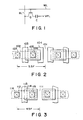
- Fig. 1 shows a memory cell widely used nowadays in a DRAM.
- the memory cell comprises a MOS (insulated gate) type transistor Q acting as a transfer gate, which is connected to a word line WL and a bit line BL, and a capacitor C for information storage having a capacitor plate potential VPL connected to one end thereof.
- MOS insulated gate
- the cells developed in an attempt to enhance the integration density of the DRAM cell of such a one transistor-one capacitor type include (a) a trench cell which utilizes a capacitor formed inside a trench formed on a substrate surface, and (b) a stacked cell constructed such that a capacitor comprising polysilicon films and an insulating film interposed between the polysilicon films is stacked on a transfer gate. Further, proposed is a cross point type cell constructed such that a single MOS transistor acting as a transfer gate and a single capacitor for information storage are arranged in a vertical direction, as disclosed in 1986 ISSCC Digest of Tech. Papers, pp. 268-269," A 4Mb DRAM with Cross-point Trech Transistor Cell "by A. SHAH et al.
- An object of the present invention is to provide a semiconductor memory device which permits overcoming the above-noted difficulties inherent in the conventional DRAM cell.
- the pattern area per bit of the cell of the present invention is markedly smaller than that of the conventional one transistor-one capacitor type DRAM cell, leading to a high integration density and a marked reduction in the unit cost per bit of the memory cell.
- the present invention provides a semiconductor memory device as set out ir claim 1.
- the MOS transistors forming the cascade gate are sequentially turned on or off in a predetermined order so as to sequentially read information stored in the capacitors onto the read/write node. Further, the information can be sequentially written into the capacitors.
- the MOS transistors forming the cascade gate are sequentially turned on or off in a predetermined order so as to sequentially read information stored in the capacitors onto the first node. Further, the information in the second node can be sequentially written into the capacitors. In addition, it is possible to read sequentially the information from the capacitors onto the first node and to sequentially write to the information read onto the first node into the capacitors by sequentially turning the MOS transistors forming the cascade gate on or off in a predetermined order except the MOS transistor at one of the both ends of the cascade gate, said MOS transistor being kept turned off. Likewise, it is possible to sequentially read the information from the capacitors onto the second node and to sequentially write the information read onto the second node into the capacitors.
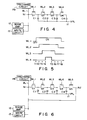
- Fig. 4 shows a semiconductor memory cell according to a first embodiment of the present invention.
- the memory cell comprises a first cascade gate consisting of a plurality of, e.g., four, cascade-connected first MOS transistors Q1 to Q4.
- One end of the first cascade gate i.e., one end of the MOS transistor Q1 in the drawing, is connected to a read/write node N1.
- capacitors C1 to C4 for information storage are connected to the first MOS transistors Q1 to Q4, respectively, at the ends remote from the node N1, so as to form a DRAM cell.
- a memory cell array formed of a plurality of the DRAM cells described above is used in a DRAM.
- the gates of the first MOS transistors Q1 to Q4 are connected to word lines WL1 to WL4 of the memory cell array, respectively, with the node N1 connected to a bit line BL of the memory cell array.
- the other ends of the capacitors C1 to C4 are commonly connected to a capacitor wiring 11 of the memory cell array.
- the plate electrodes of the capacitors C1 to C4 are commonly connected to each other, and a predetermined capacitor plate potential VPL is given to the plate electrode commonly with another DRAM cell.
- a bit line precharging circuit PR is connected to the bit line BL.
- a sense amplifier 12 senses and amplifies the potential of the bit line BL.
- a write circuit 13 serves to set the potential of the bit line BL in accordance with the data to be written.
- Fig. 5 shows timing wave forms exemplifying how the cascade gate type DRAM cell shown in Fig. 4 performs the read operation and write operation.
- the word lines WL1 to WL4 are turned on or off at the timings shown in Fig. 5 so as to sequentially turn the first MOS transistors Q1 to Q4 on in this order and the transistors Q4 to Q1 off in this order.
- the transistor Q1 is turned on, with the result that the information stored in the capacitor C1 is read through the transistor Q1 onto the bit line BL and, then, sensed by the sense amplifier 12. Then, if the word line WL2 is turned on at the time t2 after the bit line BL is precharged again for a predetermined period of time, the transistor Q2 is turned on, with the result that the information stored in the capacitor C2 is read through the transistors Q2 and Q1 onto the bit line BL.
- the transistor Q3 is turned on, with the result that the information stored in the capacitor C3 is read through the transistors Q3, Q2 and Q1 onto the bit line BL. If the word line WL4 is turned on in the next stage at the time t4 after the bit line BL is precharged again for a predetermined period of time, the transistor Q4 is turned on, with the result that the information stored in the capacitor C4 is read through the transistors Q4 and Q3 onto the bit line BL.
- the transistor Q4 is turned off so as to write the information of the bit line BL, i.e., the write data set by the write circuit 13, into the capacitor C4.
- the sense amplifier 12 can serve as the write circuit 13. If the word line WL3 is turned off in the next stage at the time t6, the transistor Q3 is turned off so as to write the information of the bit line BL into the capacitor C3. If the word line WL2 is turned off in the next stage at the time t7, the transistor Q2 is turned off so as to write the information of the bit line BL into the capacitor C2. Further, if the word line WL1 is turned off in the next stage at the time t8, the transistor Q1 is turned off so as to write the information of the bit line BL into the capacitor C1.
- the node N1 is connected to the bit line BL. However, it is possible to connect the node N1 directly to the input terminal of the sense amplifier 12.
- Fig. 6 shows a semiconductor memory cell according to a second embodiment of the present invention.
- the cascade gate type DRAM cell of the second embodiment comprises a cascade gate including a plurality of cascade-connected first MOS transistors Q1 to Q5 and connected between a first node N1 and a second node N2, and a plurality of capacitors C1 to C4 connected at one end to the connection nodes between adjacent MOS transistors, respectively.
- a memory cell array is formed of a plurality of the DRAM cells constructed as shown in Fig. 6, and is used in a DRAM.
- the gates of the MOS transistors Q1 to Q5 are connected to word lines WL1 to WL5 of the memory cell array, respectively.
- the first node N1 and the second node N2 are commonly connected to the bit line BL of the memory cell array.
- the other ends of the capacitors C1 to C4 are commonly connected to the capacitor wiring 11 of the memory cell array.
- a capacitor plate potential VPL is imparted to the capacitor wiring 11.
- the arrangement shown in Fig. 6 further comprises a bit precharging circuit PR, a sense amplifier 12 and a write circuit 13.
- Fig. 7 shows timing wave forms exemplifying how the memory cell shown in Fig. 6 performs the read operation and write operation.
- the word lines WL1 to WL5 are turned on or off at the timings shown in Fig. 7 so as to sequentially turn the first MOS transistors Q1 to Q5 on in this order and turn the transistors Q1 to Q5 off in this order. If the transistors Q1 to Q5 are sequentially turned on in this order, the information stored in the capacitors is sequentially read onto the node N1 starting with the information stored in the capacitor C1 close to the node N1 and ending with the information stored in the capacitor C4 remote from the node N1, as described previously with reference to Fig. 5.
- the word line WL1 is turned off so as to turn the transistor Q1 off, and the word line WL5 is turned on so as to turn the transistor Q5 on.
- This operation may be reversed. If the word line WL2 is turned off in the next stage at the time t5, the transistor Q2 is turned off so as to write the information of the node N2 in the capacitor C1. If the word line WL3 is turned off in the next stage at the time t6, the transistor Q3 is turned off so as to write the information of the node N2 in the capacitor C2. Further, if the word line WL4 is turned off in the next stage at the time t7, the transistor Q4 is turned off so as to write the information of the node N2 in the capacitor C3. Finally, if the word line WL5 is turned off in the next stage at the time t8, the transistor Q5 is turned off so as to write the information of the node N2 in the capacitor C4.
- first node N1 and the second node N2 are commonly connected to the same bit line BL. However, it is also possible for these first and second nodes N1 and N2 to be separately connected to different bit lines or different sense amplifiers.
- the word lines WL1 to WL5 are sequentially driven in the order opposite to that shown in Fig. 7, i.e., in the order of WL5 to WL1, so as to sequentially turn the transistors Q5 to Q1 on in this order and to sequentially turn the transistors Q5 to Q1 off in this order.
- the information stored in the capacitors is sequentially read onto the second node N2 starting with the information stored in the capacitor C4 close to the second node N2 and ending with the information stored in the capacitor C1 remote from the second node N2.
- the information of the first node. N1 is sequentially written into the capacitors starting with the capacitor C4 close to the second node N2 and ending with the capacitor C1 remote from the second node N2.
- the information can be selectively interchanged between the first node N1 and the second node N2 of the DRAM cell constructed as shown in Fig. 6, if one of the transistors Q1 and Q5 positioned at the ends of the cascade gate is kept turned off such that the remaining transistors Q2 to Q5 or Q1 to Q4 are turned on or off as described previously in conjunction with the DRAM cell shown in Fig. 4.
- the random access characteristic or the access time of the DRAM are somewhat restricted by the serial access characteristic, i.e., sequential reading and sequential writing, of the DRAM cell.
- the known DRAM performs a 4-bit serial access operation such as a nibble mode.
- a serial access characteristic is fully acceptable in the present invention.
- the random access characteristic can be completely maintained as a DRAM of x4 bit structure, if a serial-to-parallel conversion is applied to the 4-bit read/write data of the DRAM cell.
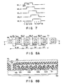
- Fig. 8A is a plan view showing the semiconductor memory cell shown in Fig. 4, which is formed as a stacked cell structure.
- the memory cell is used in a DRAM array, e.g., a DRAM cell array of an open bit line system, in which a memory node is formed at each of the intersections between the word lines and the bit line.
- Fig. 8B is a cross sectional view along the line B-B shown in Fig. 8A.
- the DRAM cell comprises a semiconductor substrate 50, a field isolation region 51, a cell active region 52 in which the active regions, i.e., source, drain and channel regions, of four transistors Q1 to Q4 are linearly arranged on the surface of the semiconductor substrate 50, gates (word lines) WL1 to WL4 of the transistors Q1 to Q4, storage nodes 531 to 534 of four capacitors C1 to C4 for information storage, contacts 541 to 544 between the storage nodes 531 to 534 and the source regions of the transistors Q1 to Q4, respectively, a contact 55 (bit line contact) between the drain region of the transistor Q1 and the bit line BL, a gate insulation film 56, an interlayer insulation film 57, an insulation film 58 for each of the capacitors C1 to C4, a plate electrode 59 for the four capacitors C1 to C4, and an interlayer insulation film 60.
- the bit line contact 55 is commonly used for another memory cell (not shown). In other words, a single bit line contact is commonly used for two memory cells (i.e., one contact per 8 bits or 1/2 contact per 4 bits).
- Fig. 2 shows the plan view of the stacked cell in the conventional DRAM cell array of the folded bit line system.
- Fig. 3 is a plan view showing the stacked cell in the conventional DRAM cell array of the open bit line system. The stacked cell shown in Fig.
- the stacked cell further comprises a plate electrode (not shown) of the capacitor for information storage.
- the stacked cell further comprises a plate electrode (not shown) of the capacitor for information storage.
- the long sides of the conventional cells in Figs. 2 and 3 are 5.5F and 4.5F, respectively.
- the long side of the pattern portion covering the transistor Q1 and the capacitor C1 is 4.5F in the DRAM cell of the present invention shown in Fig. 8A, which is substantially equal to that of the conventional cell.
- the long side of the pattern portion covering a pair of the transistor Q2 and the capacitor C2, a pair of the transistor Q3 and the capacitor C3, or a pair of the transistor Q4 and the capacitor C4 is 3F in the DRAM cell shown in Fig.
- the long side of the entire cell is 13.5F in the DRAM cell shown in Fig. 8. It follows that, in the case of a memory system of one bit per capacitor, the long side per bit of the cell is 3.375F in the present invention, which is 75% of the long side in the conventional cell shown in Fig. 3 and only 61% of the long side in the conventional cell shown in Fig. 2. Clearly, the present invention permits markedly diminishing the area per bit of the cell, leading to an improved integration density.
- each of the capacitors C1 to C4 included in the DRAM cell of the present invention shown in Fig. 8A is smaller than that of the capacitor C included in the conventional cell shown in Figs. 2 and 3.
- a capacitor capacitance Cs is diminished in the present invention, leading to an increase in a ratio Cb/Cs of a bit line capacitance Cb to the cell capacitor capacitance Cs.
- two DRAM cells are connected to the node N1 in the present invention, though only one DRAM cell is shown in the drawing. In other words, one bit line contact is used for 8 bits (1/2 bit contact line per 4 bits), with the result that the bit line capacitance Cb is also markedly diminished in the present invention.
- the capacitor capacitance Cs it is possible to increase the capacitor capacitance Cs, though a process change is required to some extent in this case, as described in, for example, "1988 IEDM Technical Digest, pp. 592-595 '3-DIMENSIONAL STACKED CAPACITOR CELL FOR 16M AND 64M DRAMS' by T. EMA et al" or "Stacked Capacitor Cells for High-density Dynamic RAMs" by H. WATANABE et al on pp. 600-603 of the literature noted above.
- the array is constructed to include one bit at every intersection between the bit line and the word lines.
- the DRAM cell of the present invention shown in Figs. 8A and 8B is of a stacked cell structure.
- the present invention also permits providing a DRAM cell of a cross point cell structure by employing the technique described in, for example, "1989 IEDM Technical Digest, pp. 23-26, 'A Surrounding Gate Transistor (SGT) Cell for 64/256Mbit DRAMs' by K. SUNOUCHI et al.
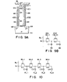
- Fig. 9A is a cross sectional view exemplifying a DRAM cell of the present invention utilizing a cross point cell structure.
- Fig. 9B is an equivalent circuit diagram of the cell shown in Fig. 9A.
- a pair of a vertical transistor and a vertical capacitor is stacked upon another pair in the vertical direction. It should be noted that the bit portion covering the number of pairs of the stacked vertical transistors and vertical capacitors can be integrated into a cell size equal to the one bit portion in the prior art.
- the DRAM cell comprises a p-type semiconductor substrate 61 having a convex portion partially formed on the surface, an n + -type drain region 62 of a transistor Q1 formed on the upper surface of the convex portion of the substrate 61, gate (word line) 631 (WL1) of the transistor Q1, gate (word line) 632 (WL2) of the transistor Q2 formed in the side surfaces of the convex portion of the substrate with gate insulation films interposed between these gates and the substrate, n + -type conductive layers 64, i.e., the source region of the transistor Q1, storage node of a capacitor C1, drain region of a transistor Q2, partially formed on the side surface of the convex portion of the substrate 61, an n + -type source region 65 of the transistor Q2 formed in the lower end portions of the side surfaces of the convex portion of the substrate, a plate electrode 66 of a capacitor C1 or C2 partially formed on the side surface of the convex portion of the substrate with a gate insulation
- each of the DRAM cells shown in Fig. 4 and 6 the other ends of the capacitors C1 to C4 are commonly connected to the capacitor plate potential VPL. However, it is also possible to connect each of the other ends of the capacitors C1 to C4 to a power source potential V CC given from the outside or to the ground potential V SS .
- Fig. 10 is an equivalent circuit diagram of the DRAM cell prepared by applying the technique described in this literature to, for example, the DRAM cell shown in Fig. 4. In this case, capacitor wirings PL1 to PL4 are connected to the other ends of the capacitors C1 to C4, respectively, as shown in Fig. 10.
- Fig. 11 is an equivalent circuit diagram of the DRAM cell prepared by applying the technique described in this literature to the DRAM cell shown in Fig. 4.
- Fig. 12 is an equivalent circuit diagram of the DRAM cell prepared by applying the technique described in this literature to the DRAM cell shown in Fig. 6.
- the DRAM cell shown in Fig. 11 comprises cascade-connected second MOS transistors Q1' to Q4' acting as transfer gates.
- the sources of these transistors Q1' to Q4' are connected to the other ends of the capacitors C1 to C4, respectively, and the gates of these second transistors Q1' to Q4' are connected to the gates of the first transistors Q1 to Q4, respectively.
- the drains of the first and second transistors Q1 and Q1' are connected to complementary bit lines BL and BL ⁇ , respectively. Incidentally, it is possible to connect the drains of these transistors Q1 and Q1' directly to a pair of differential input terminals of the sense amplifier.
- the DRAM cell shown in Fig. 12 comprises cascade-connected second MOS transistors Q1' to Q5' acting as transfer gates.
- the connection nodes between adjacent second transistors are connected to the other ends of the capacitors C1 to C4, respectively.
- the gates of the second transistors Q1' to Q5' are connected to the gates of the first trasistors Q1 to Q5, respectively.
- the first and second transistors Q1 and Q1' are connected at one end to complementary bit lines BL1 and BL1 ⁇ , respectively.
- the first and second transistors Q5 and Q5' are connected at the other end to complementary bit lines BL2, BL2 ⁇ , respectively.
- the DRAM cell is constructed such that one bit signal of "1" or "0" (one digital data) is stored in a single capacitor.
- the DRAM cell it is possible to construct the DRAM cell such that data consisting of a plurality of bits is stored in a single capacitor.
- the semiconductor memory cell of the present invention permits markedly diminishing the cell area per bit using the conventional process technology, leading to a marked reduction in the unit cost per bit. It follows that the present invention makes it possible to avoid the problem inherent in the prior art, i.e., the problem that the manufacturing process is made highly complex and the manufacturing time is increased with increase in the integration density. Further, if a new process technique is developed, the integration density can be further enhanced drastically by the present invention. Naturally, the present invention is highly advantageous in the case of manufacturing a DRAM of a large capacity at a low cost for use as a substitute for memory media such as a magnetic disk.
Description
- The present invention relates to a semiconductor memory device, particularly, to a memory device used in, for example, a dynamic random access memory (DRAM).
- Fig. 1 shows a memory cell widely used nowadays in a DRAM. As shown in the drawing, the memory cell comprises a MOS (insulated gate) type transistor Q acting as a transfer gate, which is connected to a word line WL and a bit line BL, and a capacitor C for information storage having a capacitor plate potential VPL connected to one end thereof.
- The cells developed in an attempt to enhance the integration density of the DRAM cell of such a one transistor-one capacitor type include (a) a trench cell which utilizes a capacitor formed inside a trench formed on a substrate surface, and (b) a stacked cell constructed such that a capacitor comprising polysilicon films and an insulating film interposed between the polysilicon films is stacked on a transfer gate. Further, proposed is a cross point type cell constructed such that a single MOS transistor acting as a transfer gate and a single capacitor for information storage are arranged in a vertical direction, as disclosed in 1986 ISSCC Digest of Tech. Papers, pp. 268-269," A 4Mb DRAM with Cross-point Trech Transistor Cell "by A. SHAH et al.
- However, the conventional memory cells outlined above necessitate a highly complex manufacturing process and a long manufacturing time. It is considered very difficult to overcome these difficulties as a result of researches on the trench cell, etc. noted above.
- Features corresponding to those of the preamble of
claim 1 are known from DE-B-1 922 761. - An object of the present invention is to provide a semiconductor memory device which permits overcoming the above-noted difficulties inherent in the conventional DRAM cell. The pattern area per bit of the cell of the present invention is markedly smaller than that of the conventional one transistor-one capacitor type DRAM cell, leading to a high integration density and a marked reduction in the unit cost per bit of the memory cell.
- To achieve the object noted above, the present invention provides a semiconductor memory device as set out ir
claim 1. - In the semiconductor memory cell of the present invention, the MOS transistors forming the cascade gate are sequentially turned on or off in a predetermined order so as to sequentially read information stored in the capacitors onto the read/write node. Further, the information can be sequentially written into the capacitors.
- In the memory device of the construction as set out in
claim 13, the MOS transistors forming the cascade gate are sequentially turned on or off in a predetermined order so as to sequentially read information stored in the capacitors onto the first node. Further, the information in the second node can be sequentially written into the capacitors. In addition, it is possible to read sequentially the information from the capacitors onto the first node and to sequentially write to the information read onto the first node into the capacitors by sequentially turning the MOS transistors forming the cascade gate on or off in a predetermined order except the MOS transistor at one of the both ends of the cascade gate, said MOS transistor being kept turned off. Likewise, it is possible to sequentially read the information from the capacitors onto the second node and to sequentially write the information read onto the second node into the capacitors. - This invention can be more fully understood from the following detailed description when taken in conjunction with the accompanying drawings, in which:
- Fig. 1 is an equivalent circuit diagram showing the construction of a conventional DRAM cell of one transistor-one capacitor type;
- Fig. 2 is a plan view showing the construction of a stacked cell of one transistor-one capacitor type included in a DRAM cell array of a conventional folded bit line system;
- Fig. 3 is a plan view showing the construction of a stacked cell of one transistor-one capacitor type included in a DRAM cell array of a conventional open bit line system;
- Fig. 4 is an equivalent circuit diagram showing a semiconductor memory cell according to one embodiment of the present invention;
- Fig. 5 shows wave forms denoting as an example the timing of the read operation and write operation of the memory cell shown in Fig. 4;
- Fig. 6 is an equivalent circuit diagram showing a semiconductor memory cell according to another embodiment of the present invention;
- Fig. 7 shows wave forms denoting as an example the timing of the read operation and write operation of the memory cell shown in Fig. 6;
- Fig. 8A is a plan view showing that a stacked cell structure is employed in the semiconductor memory cell shown in Fig. 4;
- Fig. 8B is a cross sectional view along the line B-B shown in Fig. 8A;
- Fig. 9A is a cross sectional view showing an example of the semiconductor memory cell of the present invention employing a cross point cell structure;
- Fig. 9B is an equivalent circuit diagram showing the semiconductor memory cell shown in Fig. 9A;
- Fig. 10 is an equivalent circuit diagram showing a modification of the memory cell shown in Fig. 4;
- Fig. 11 is an equivalent circuit diagram showing another modification of the memory cell shown in Fig. 4; and
- Fig. 12 is an equivalent circuit diagram showing a modification of the memory cell shown in Fig. 6.
- The accompanying drawings show some embodiments of the present invention. Throughout the drawings, like reference numerals denote the like members of the semiconductor memory cell.
- Specifically, Fig. 4 shows a semiconductor memory cell according to a first embodiment of the present invention. As seen from the drawing, the memory cell comprises a first cascade gate consisting of a plurality of, e.g., four, cascade-connected first MOS transistors Q1 to Q4. One end of the first cascade gate, i.e., one end of the MOS transistor Q1 in the drawing, is connected to a read/write node N1. Further, capacitors C1 to C4 for information storage are connected to the first MOS transistors Q1 to Q4, respectively, at the ends remote from the node N1, so as to form a DRAM cell.
- A memory cell array formed of a plurality of the DRAM cells described above is used in a DRAM. In this case, the gates of the first MOS transistors Q1 to Q4 are connected to word lines WL1 to WL4 of the memory cell array, respectively, with the node N1 connected to a bit line BL of the memory cell array. Further, the other ends of the capacitors C1 to C4 are commonly connected to a
capacitor wiring 11 of the memory cell array. In this embodiment, the plate electrodes of the capacitors C1 to C4 are commonly connected to each other, and a predetermined capacitor plate potential VPL is given to the plate electrode commonly with another DRAM cell. As seen from the drawing, a bit line precharging circuit PR is connected to the bit line BL. A sense amplifier 12 senses and amplifies the potential of the bit line BL. Further, awrite circuit 13 serves to set the potential of the bit line BL in accordance with the data to be written. - Fig. 5 shows timing wave forms exemplifying how the cascade gate type DRAM cell shown in Fig. 4 performs the read operation and write operation. In this embodiment, the word lines WL1 to WL4 are turned on or off at the timings shown in Fig. 5 so as to sequentially turn the first MOS transistors Q1 to Q4 on in this order and the transistors Q4 to Q1 off in this order. To be more specific, if the word line WL1 is turned on at the time t1 after precharging of the bit line BL to a predetermined potential by the bit line precharging circuit PR, the transistor Q1 is turned on, with the result that the information stored in the capacitor C1 is read through the transistor Q1 onto the bit line BL and, then, sensed by the
sense amplifier 12. Then, if the word line WL2 is turned on at the time t2 after the bit line BL is precharged again for a predetermined period of time, the transistor Q2 is turned on, with the result that the information stored in the capacitor C2 is read through the transistors Q2 and Q1 onto the bit line BL. If the word line WL3 is turned on in the next stage at the time t3 after the bit line BL is precharged again for a predetermined period of time, the transistor Q3 is turned on, with the result that the information stored in the capacitor C3 is read through the transistors Q3, Q2 and Q1 onto the bit line BL. If the word line WL4 is turned on in the next stage at the time t4 after the bit line BL is precharged again for a predetermined period of time, the transistor Q4 is turned on, with the result that the information stored in the capacitor C4 is read through the transistors Q4 and Q3 onto the bit line BL. Further, if the word line WL4 is turned off at the time t5, the transistor Q4 is turned off so as to write the information of the bit line BL, i.e., the write data set by thewrite circuit 13, into the capacitor C4. Thesense amplifier 12 can serve as thewrite circuit 13. If the word line WL3 is turned off in the next stage at the time t6, the transistor Q3 is turned off so as to write the information of the bit line BL into the capacitor C3. If the word line WL2 is turned off in the next stage at the time t7, the transistor Q2 is turned off so as to write the information of the bit line BL into the capacitor C2. Further, if the word line WL1 is turned off in the next stage at the time t8, the transistor Q1 is turned off so as to write the information of the bit line BL into the capacitor C1. - It is possible to rearrange the order of reading data, to correct an error, etc. during the series of the reading operation and the series of the writing operation described above, i.e., between the times t4 and t5 shown in Fig. 5.
- In the cascade gate type DRAM cell as shown in Fig. 4, it is possible to sequentially read onto the node N1 the information stored in the capacitors in the order starting with the information stored in the capacitor C1 positioned close to the node N1 and ending with the information stored in the capacitor C4 remote from the node N1 by sequentially turning the transistors Q1 to Q4 in a predetermined order. It is also possible to sequentially write the information of the node N1 into the capacitors starting with the capacitor C4 remote from the node N1 and ending with the capacitor C1 close to the node N1.
- In the embodiment shown in Fig. 4, the node N1 is connected to the bit line BL. However, it is possible to connect the node N1 directly to the input terminal of the
sense amplifier 12. - Fig. 6 shows a semiconductor memory cell according to a second embodiment of the present invention. As seen from the drawing, the cascade gate type DRAM cell of the second embodiment comprises a cascade gate including a plurality of cascade-connected first MOS transistors Q1 to Q5 and connected between a first node N1 and a second node N2, and a plurality of capacitors C1 to C4 connected at one end to the connection nodes between adjacent MOS transistors, respectively. In this embodiment, it is necessary to use at least three MOS transistors forming the cascade gate, though five MOS transistors are shown in the drawing.
- A memory cell array is formed of a plurality of the DRAM cells constructed as shown in Fig. 6, and is used in a DRAM. The gates of the MOS transistors Q1 to Q5 are connected to word lines WL1 to WL5 of the memory cell array, respectively. The first node N1 and the second node N2 are commonly connected to the bit line BL of the memory cell array. The other ends of the capacitors C1 to C4 are commonly connected to the
capacitor wiring 11 of the memory cell array. In this embodiment, a capacitor plate potential VPL is imparted to thecapacitor wiring 11. The arrangement shown in Fig. 6 further comprises a bit precharging circuit PR, asense amplifier 12 and awrite circuit 13. - Fig. 7 shows timing wave forms exemplifying how the memory cell shown in Fig. 6 performs the read operation and write operation. In this embodiment, the word lines WL1 to WL5 are turned on or off at the timings shown in Fig. 7 so as to sequentially turn the first MOS transistors Q1 to Q5 on in this order and turn the transistors Q1 to Q5 off in this order. If the transistors Q1 to Q5 are sequentially turned on in this order, the information stored in the capacitors is sequentially read onto the node N1 starting with the information stored in the capacitor C1 close to the node N1 and ending with the information stored in the capacitor C4 remote from the node N1, as described previously with reference to Fig. 5. Then, the word line WL1 is turned off so as to turn the transistor Q1 off, and the word line WL5 is turned on so as to turn the transistor Q5 on. This operation may be reversed. If the word line WL2 is turned off in the next stage at the time t5, the transistor Q2 is turned off so as to write the information of the node N2 in the capacitor C1. If the word line WL3 is turned off in the next stage at the time t6, the transistor Q3 is turned off so as to write the information of the node N2 in the capacitor C2. Further, if the word line WL4 is turned off in the next stage at the time t7, the transistor Q4 is turned off so as to write the information of the node N2 in the capacitor C3. Finally, if the word line WL5 is turned off in the next stage at the time t8, the transistor Q5 is turned off so as to write the information of the node N2 in the capacitor C4.
- It is possible to rearrange the order of reading data, to correct an error, etc. during the series of the reading operation and the series of the writing operation described above, i.e., between the times t4 and t5 shown in Fig. 7.
- In the cascade gate type DRAM cell as shown in Fig. 6, it is possible to sequentially read onto the first node N1 the information stored in the capacitors in the order starting with the information stored in the capacitor C1 positioned close to the node N1 and ending with the information stored in the capacitor C4 remote from the node N1 by sequentially turning the transistors Q1 to Q5 in a predetermined order. It is also possible to sequentially write the information of the node N2 into the capacitors in the order starting with the capacitor C1 close to the node N1 and ending with the capacitor C4 remote from to the node N1.
- In the embodiment shown in Fig. 6, the first node N1 and the second node N2 are commonly connected to the same bit line BL. However, it is also possible for these first and second nodes N1 and N2 to be separately connected to different bit lines or different sense amplifiers.
- Suppose the word lines WL1 to WL5 are sequentially driven in the order opposite to that shown in Fig. 7, i.e., in the order of WL5 to WL1, so as to sequentially turn the transistors Q5 to Q1 on in this order and to sequentially turn the transistors Q5 to Q1 off in this order. In this case, the information stored in the capacitors is sequentially read onto the second node N2 starting with the information stored in the capacitor C4 close to the second node N2 and ending with the information stored in the capacitor C1 remote from the second node N2. Also, the information of the first node. N1 is sequentially written into the capacitors starting with the capacitor C4 close to the second node N2 and ending with the capacitor C1 remote from the second node N2.
- It should also be noted that the information can be selectively interchanged between the first node N1 and the second node N2 of the DRAM cell constructed as shown in Fig. 6, if one of the transistors Q1 and Q5 positioned at the ends of the cascade gate is kept turned off such that the remaining transistors Q2 to Q5 or Q1 to Q4 are turned on or off as described previously in conjunction with the DRAM cell shown in Fig. 4.
- If an array of the cascade gate type DRAM cells of the present invention describe above is used for forming a DRAM, the random access characteristic or the access time of the DRAM are somewhat restricted by the serial access characteristic, i.e., sequential reading and sequential writing, of the DRAM cell. However, the known DRAM performs a 4-bit serial access operation such as a nibble mode. Of course, such a serial access characteristic is fully acceptable in the present invention. Also, in the case of forming a DRAM, the random access characteristic can be completely maintained as a DRAM of x4 bit structure, if a serial-to-parallel conversion is applied to the 4-bit read/write data of the DRAM cell. In addition, it is possible to achieve a DRAM of x8 bit structure or x16 bit structure by the serial-to-parallel conversion, in the case where the memory cell array is divided into a plurality of sub-arrays and some sub-arrays alone, e.g., 2 to 4 sub-arrays, are simultaneously activated for the purpose of power saving. Further, the field of DRAM application, in which it suffices to employ the serial access such as the block transfer between the DRAM and a cash memory as well as the processing and holding of data for picture image, is rapidly widened in recent years. Under the circumstances, the restriction of the random access characteristic noted above does not obstruct at all the improvement in the integration density achieved by the present invention.
- The cascade gate type DRAM cell of the present invention is constructed as shown in, for example, Fig. 8. Specifically, Fig. 8A is a plan view showing the semiconductor memory cell shown in Fig. 4, which is formed as a stacked cell structure. The memory cell is used in a DRAM array, e.g., a DRAM cell array of an open bit line system, in which a memory node is formed at each of the intersections between the word lines and the bit line. Fig. 8B is a cross sectional view along the line B-B shown in Fig. 8A.
- As shown in the drawings, the DRAM cell comprises a
semiconductor substrate 50, afield isolation region 51, a cellactive region 52 in which the active regions, i.e., source, drain and channel regions, of four transistors Q1 to Q4 are linearly arranged on the surface of thesemiconductor substrate 50, gates (word lines) WL1 to WL4 of the transistors Q1 to Q4,storage nodes 531 to 534 of four capacitors C1 to C4 for information storage,contacts 541 to 544 between thestorage nodes 531 to 534 and the source regions of the transistors Q1 to Q4, respectively, a contact 55 (bit line contact) between the drain region of the transistor Q1 and the bit line BL, agate insulation film 56, aninterlayer insulation film 57, aninsulation film 58 for each of the capacitors C1 to C4, aplate electrode 59 for the four capacitors C1 to C4, and aninterlayer insulation film 60. - The
bit line contact 55 is commonly used for another memory cell (not shown). In other words, a single bit line contact is commonly used for two memory cells (i.e., one contact per 8 bits or 1/2 contact per 4 bits). - For comparison of the pattern area between the cascade gate type DRAM cell of the present invention shown in Figs. 8A, 8B and the conventional one transistor-one capacitor type DRAM cell, Fig. 2 shows the plan view of the stacked cell in the conventional DRAM cell array of the folded bit line system. Fig. 3 is a plan view showing the stacked cell in the conventional DRAM cell array of the open bit line system. The stacked cell shown in Fig. 2 comprises a
field isolation region 101, anactive region 102 of a transistor for transfer gate, a gate (word line) 103 of the transistor, aword line 104 for another transistor (not shown), astorage node 105 of the capacitor for information storage, acontact 106 between thestorage node 106 and the source region of the transistor, and acontact 107 between the drain region of the transistor and a bit line (not shown). The stacked cell further comprises a plate electrode (not shown) of the capacitor for information storage. On the other hand, the stacked cell shown in Fig. 3 comprises a field isolation region 111, anactive region 112 of a transistor for transfer gate, a gate (word line) 113 of the transistor, astorage node 114 of a capacitor for information storage, acontact 115 between thestorage node 114 and the source region of the transistor, and a contact 116 (bit line contact) between the drain region of the transistor and a bit line (not shown). The stacked cell further comprises a plate electrode (not shown) of the capacitor for information storage. - Where the allowance for aligning a mask pattern is set at 0.5F ("F" denoting the minimum size in the manufacturing process of the cell) in the DRAM cell shown in each of Figs. 2 and 3, the long sides of the conventional cells in Figs. 2 and 3 are 5.5F and 4.5F, respectively. On the other hand, the long side of the pattern portion covering the transistor Q1 and the capacitor C1 is 4.5F in the DRAM cell of the present invention shown in Fig. 8A, which is substantially equal to that of the conventional cell. However, the long side of the pattern portion covering a pair of the transistor Q2 and the capacitor C2, a pair of the transistor Q3 and the capacitor C3, or a pair of the transistor Q4 and the capacitor C4 is 3F in the DRAM cell shown in Fig. 8A. In other words, the long side of the entire cell is 13.5F in the DRAM cell shown in Fig. 8. It follows that, in the case of a memory system of one bit per capacitor, the long side per bit of the cell is 3.375F in the present invention, which is 75% of the long side in the conventional cell shown in Fig. 3 and only 61% of the long side in the conventional cell shown in Fig. 2. Clearly, the present invention permits markedly diminishing the area per bit of the cell, leading to an improved integration density.
- It should also be noted that the area of each of the capacitors C1 to C4 included in the DRAM cell of the present invention shown in Fig. 8A is smaller than that of the capacitor C included in the conventional cell shown in Figs. 2 and 3. This may suggest that a capacitor capacitance Cs is diminished in the present invention, leading to an increase in a ratio Cb/Cs of a bit line capacitance Cb to the cell capacitor capacitance Cs. However, two DRAM cells are connected to the node N1 in the present invention, though only one DRAM cell is shown in the drawing. In other words, one bit line contact is used for 8 bits (1/2 bit contact line per 4 bits), with the result that the bit line capacitance Cb is also markedly diminished in the present invention. It follows that the value of Cb/Cs ratio is smaller in the present invention than in the prior art, leading to a larger change in the bit line potential in the data reading step. What should also be noted is that the marked reduction in the bit line capacitance Cb permits saving of power consumption.
- Incidentally, it is possible to increase the capacitor capacitance Cs, though a process change is required to some extent in this case, as described in, for example, "1988 IEDM Technical Digest, pp. 592-595 '3-DIMENSIONAL STACKED CAPACITOR CELL FOR 16M AND 64M DRAMS' by T. EMA et al" or "Stacked Capacitor Cells for High-density Dynamic RAMs" by H. WATANABE et al on pp. 600-603 of the literature noted above. In this case, the array is constructed to include one bit at every intersection between the bit line and the word lines.
- The DRAM cell of the present invention shown in Figs. 8A and 8B is of a stacked cell structure. However, the present invention also permits providing a DRAM cell of a cross point cell structure by employing the technique described in, for example, "1989 IEDM Technical Digest, pp. 23-26, 'A Surrounding Gate Transistor (SGT) Cell for 64/256Mbit DRAMs' by K. SUNOUCHI et al.
- Fig. 9A is a cross sectional view exemplifying a DRAM cell of the present invention utilizing a cross point cell structure. On the other hand, Fig. 9B is an equivalent circuit diagram of the cell shown in Fig. 9A. In this embodiment, a pair of a vertical transistor and a vertical capacitor is stacked upon another pair in the vertical direction. It should be noted that the bit portion covering the number of pairs of the stacked vertical transistors and vertical capacitors can be integrated into a cell size equal to the one bit portion in the prior art. As seen from the drawings, the DRAM cell comprises a p-type semiconductor substrate 61 having a convex portion partially formed on the surface, an n+-type drain region 62 of a transistor Q1 formed on the upper surface of the convex portion of the substrate 61, gate (word line) 631 (WL1) of the transistor Q1, gate (word line) 632 (WL2) of the transistor Q2 formed in the side surfaces of the convex portion of the substrate with gate insulation films interposed between these gates and the substrate, n+-type conductive layers 64, i.e., the source region of the transistor Q1, storage node of a capacitor C1, drain region of a transistor Q2, partially formed on the side surface of the convex portion of the substrate 61, an n+-type source region 65 of the transistor Q2 formed in the lower end portions of the side surfaces of the convex portion of the substrate, a plate electrode 66 of a capacitor C1 or C2 partially formed on the side surface of the convex portion of the substrate with a gate insulation film interposed between the plate 66 and the substrate, a bit line BL, a contact 67 (bit line contact) between the bit line BL and the drain region 62 of the transistor Q1, and a p+-type element isolation region 68.
- In each of the DRAM cells shown in Fig. 4 and 6, the other ends of the capacitors C1 to C4 are commonly connected to the capacitor plate potential VPL. However, it is also possible to connect each of the other ends of the capacitors C1 to C4 to a power source potential VCC given from the outside or to the ground potential VSS.
- It is also possible to achieve the DRAM cell of the present invention by utilizing the technique of allowing the capacitor plate to perform the clock operation, as described in "IEEE JOURNAL OF SOLID-STATE CIRCUITS, VOL. SC-17, NO. 5, p-872, Oct. 1982, 'A Storage-Node-Boosted RAM with Word-Line Delay Compensation' by K. FUJISHIMA et al". Fig. 10 is an equivalent circuit diagram of the DRAM cell prepared by applying the technique described in this literature to, for example, the DRAM cell shown in Fig. 4. In this case, capacitor wirings PL1 to PL4 are connected to the other ends of the capacitors C1 to C4, respectively, as shown in Fig. 10.
- It is also possible to achieve the DRAM cell of the present invention by utilizing the technique of connecting transfer gates to both ends of each of the capacitors, as described in "1989 Symposium of VLSI Circuits, Digest of Tech. Papers, pp. 101-102, 'A Novel Memory Cell Architecture for High-Density DRAMs', Fig. 1(b), by Y. OHTA et al." Fig. 11 is an equivalent circuit diagram of the DRAM cell prepared by applying the technique described in this literature to the DRAM cell shown in Fig. 4. On the other hand, Fig. 12 is an equivalent circuit diagram of the DRAM cell prepared by applying the technique described in this literature to the DRAM cell shown in Fig. 6.
- The DRAM cell shown in Fig. 11 comprises cascade-connected second MOS transistors Q1' to Q4' acting as transfer gates. The sources of these transistors Q1' to Q4' are connected to the other ends of the capacitors C1 to C4, respectively, and the gates of these second transistors Q1' to Q4' are connected to the gates of the first transistors Q1 to Q4, respectively. Further, the drains of the first and second transistors Q1 and Q1' are connected to complementary bit lines BL and

- The DRAM cell shown in Fig. 12 comprises cascade-connected second MOS transistors Q1' to Q5' acting as transfer gates. In this embodiment, the connection nodes between adjacent second transistors are connected to the other ends of the capacitors C1 to C4, respectively. Also, the gates of the second transistors Q1' to Q5' are connected to the gates of the first trasistors Q1 to Q5, respectively. The first and second transistors Q1 and Q1' are connected at one end to complementary bit lines BL1 and


- In each of the embodiments described above, the DRAM cell is constructed such that one bit signal of "1" or "0" (one digital data) is stored in a single capacitor. However, it is possible to construct the DRAM cell such that data consisting of a plurality of bits is stored in a single capacitor.
- As described above in detail, the semiconductor memory cell of the present invention permits markedly diminishing the cell area per bit using the conventional process technology, leading to a marked reduction in the unit cost per bit. It follows that the present invention makes it possible to avoid the problem inherent in the prior art, i.e., the problem that the manufacturing process is made highly complex and the manufacturing time is increased with increase in the integration density. Further, if a new process technique is developed, the integration density can be further enhanced drastically by the present invention. Naturally, the present invention is highly advantageous in the case of manufacturing a DRAM of a large capacity at a low cost for use as a substitute for memory media such as a magnetic disk.
- The present invention is not restricted by the embodiments described with reference to the accompanying drawings. In other words, various modifications are available within the technical scope of the present invention.
- Reference signs in the claims are intended for better understanding and shall not limit the scope.
Claims (21)
- A semiconductor memory device, comprising a first cascade gate including a plurality of cascade-connected first MOS transistors (Q1 to Q4) and having one end connected to a first node (N1), and a plurality of capacitors (C1 to C4) for information storage connected at one end to said first MOS transistors (Q1 to Q4), respectively, at the end of each transistor remote from said first node (N1), characterised in that:
the memory device comprises means for reading data from the plurality of cells in sequence starting with that one which is closest to the first node (N1) with only those first MOS transistors (Q1-Q4) made conductive which are arranged between the first node and the capacitor of the addressed cell. - The semiconductor memory devise of claim 1 characterised by
means for writing data into the plurality of cells in sequence starting with that one which is remote from the first node (N1) with only those first MOS transistors made conductive which are arranged between the first node and the capacitor of the addressed cell. - The semiconductor memory device according to claim 1 or claim 2, characterised in that the gates of the first MOS transistors (Q1 to Q4) are connected respectively to word lines (WL1 to WL4) of a memory cell array, and the first MOS transistors (Q1 to Q4) are turned on or off in a predetermined order.
- The semiconductor memory device according to claim 1 or claim 2, characterised in that the first node (N1) is connected to a bit line (BL) of the memory cell array.
- The semiconductor memory device according to claim 1 or claim 2, characterised in that the other ends of the capacitors (C1 to C4) are commonly connected to a wiring (11).
- The semiconductor memory device according to claim 1 or claim 2, characterised in that the plate electrodes of the capacitors (C1 to C4) are commonly formed, and a predetermined capacitor plate potential is given to said common plate electrode.
- The semiconductor memory device according to claim 1 or claim 2, characterised in that the other ends of the capacitors (C1 to C4) are connected to different wirings (PL1 to PL4), respectively.
- The semiconductor memory device according to claim 1 or claim 2, characterised in that the memory cell further comprises a second cascade gate including a plurality of cascade-connected second MOS transistors (Q1' to Q4'), the number of said second MOS transistors (Q1' to Q4'), being equal to that of first MOS transistors (Q1 to Q4), the other ends of the second MOS transistors (Q1' to Q4') being connected to the other ends of the capacitors (C1 to C4), respectively, and the gates of the second MOS transistors (Q1' to Q4') being connected to the gates of the first MOS transistors (Q1 to Q4), respectively.
- The semiconductor memory device according to claim 8, characterised in that the first node (N1) and one end of the second cascade gate are connected to complementary bit lines (BL,

- The semiconductor memory device according to claim 1 or 2, and comprising a stacked cell structure constructed such that the source, drain and channel regions of each of the first MOS transistors (Q1 to Q4) are linearly arranged on the semiconductor substrate surface, and storage nodes of the capacitors (C1 to C4) are in contact with the source regions or drain regions of the first MOS transistors (Q1 to Q4), respectively.
- A semiconductor memory device, characterised in that the semiconductor memory cell defined in claim 10 comprises four first MOS transistors (Q1 to Q4) and four capacitors (C1 to C4).
- A semiconductor memory device according to claim 1 or 2, and comprising a cross-point cell structure constructed such that the first MOS transistors (Q1 to Q4) and the capacitors (C1 to C4) are at least partially stacked one upon the other in the vertical direction.
- A semiconductor memory device as defined in any of claims 1, 2, 3, 5 to 7 or 12 wherein the first cascade gate includes at least three cascade-connected first MOS transistors (Q1 to Q5) interposed between the first node (N1) for reading and a second node (N2) for writing, and the plurality of capacitors (C1 to C4) for information storage connected at one end to the connection nodes between adjacent first MOS transistors forming said first cascade gate, respectively, and
the device comprises means for writing data into the plurality of cells in sequence starting with that one which is remote from the second node (N2), with only those first MOS transistors made conductive which are arranged between the second node and the capacitor of the addressed cell. - The semiconductor memory device according to claim 13, characterised in that the memory cell further comprises a second cascade gate including a plurality of cascade-connected second MOS transistors (Q1' to Q5'), the number of said second MOS transistors (Q1' to Q5') being equal to that of first MOS transistors (Q1 to Q5), the connection nodes between adjacent second MOS transistors (Q1' to Q5') being connected to the other ends of the capacitors (C1 to C4), respectively, and the gates of the second MOS transistors (Q1' to Q5') being connected to the gates of the first MOS transistors (Q1 to Q5), respectively.
- The semiconductor memory device according to claim 14, characterised in that the first node (N1) and one end of the second cascade gate are connected to complementary bit lines (BL1,


- The semiconductor memory device according to claim 13, and comprising a stacked cell structure constructed such that the source, drain and channel regions of each of the cascade-connected first MOS transistors (Q1 to Q5) are linearly arranged on the semiconductor substrate surface, and the storage nodes (531 to 534) of the capacitors (C1 to C4) are in contact with the source-drain regions of the cascade-connected first MOS transistors, respectively.
- The semiconductor memory device according to claim 16, characterised in that the cell structure comprises five first MOS transistors (Q1 to Q5) and four capacitors (C1 to C4).
- The semiconductor memory device according to claim 13, characterised in that the gates of the first MOS transistors (Q1 to Q5) are connected to different word lines (WL1 to WL5) of the memory cell array, respectively, and one of the first MOS transistors at the ends of the cascade gate is selectively kept off so as to permit the other first MOS transistors (Q2 to Q5, or Q1 to Q4) to be turned on or off in a predetermined order.
- The semiconductor memory device according to any of claims 13 or 16 to 18, characterised in that the first node (N1) and the second node (N2) are commonly connected to each other.
- The semiconductor memory device according to claim 14, characterised in that the first node (N1) and the second node (N2) are commonly connected to each other, and one end and the other end of the second cascade gate are commonly connected to each other.
- The semiconductor memory device according to claim 20, characterised in that the commonly connected point between the first node (N1) and the second node (N2) is connected to a bit line (BL1) of the memory cell array, and the commonly connected point between one end and the other end of the second cascade gate is connected to another bit line

Applications Claiming Priority (2)
| Application Number | Priority Date | Filing Date | Title |
|---|---|---|---|
| JP104576/90 | 1990-04-20 | ||
| JP2104576A JPH0834257B2 (en) | 1990-04-20 | 1990-04-20 | Semiconductor memory cell |
Publications (3)
| Publication Number | Publication Date |
|---|---|
| EP0453959A2 EP0453959A2 (en) | 1991-10-30 |
| EP0453959A3 EP0453959A3 (en) | 1992-10-28 |
| EP0453959B1 true EP0453959B1 (en) | 1996-09-04 |
Family
ID=14384265
Family Applications (1)
| Application Number | Title | Priority Date | Filing Date |
|---|---|---|---|
| EP91106207A Expired - Lifetime EP0453959B1 (en) | 1990-04-20 | 1991-04-18 | Semiconductor memory cell |
Country Status (5)
| Country | Link |
|---|---|
| US (1) | US5525820A (en) |
| EP (1) | EP0453959B1 (en) |
| JP (1) | JPH0834257B2 (en) |
| KR (1) | KR930008008B1 (en) |
| DE (1) | DE69121760T2 (en) |
Families Citing this family (35)
| Publication number | Priority date | Publication date | Assignee | Title |
|---|---|---|---|---|
| DE69225044T2 (en) * | 1991-11-18 | 1998-10-22 | Toshiba Kawasaki Kk | Dynamic semiconductor memory device |
| JP3464803B2 (en) * | 1991-11-27 | 2003-11-10 | 株式会社東芝 | Semiconductor memory cell |
| JP3322936B2 (en) * | 1992-03-19 | 2002-09-09 | 株式会社東芝 | Semiconductor storage device |
| KR950012731A (en) * | 1993-10-25 | 1995-05-16 | 사토 후미오 | Semiconductor memory device and manufacturing method |
| US5923829A (en) | 1994-08-25 | 1999-07-13 | Ricoh Company, Ltd. | Memory system, memory control system and image processing system |
| JP2783271B2 (en) * | 1995-01-30 | 1998-08-06 | 日本電気株式会社 | Semiconductor storage device |
| US5936874A (en) * | 1997-06-19 | 1999-08-10 | Micron Technology, Inc. | High density semiconductor memory and method of making |
| US6229161B1 (en) * | 1998-06-05 | 2001-05-08 | Stanford University | Semiconductor capacitively-coupled NDR device and its applications in high-density high-speed memories and in power switches |
| US6423596B1 (en) | 1998-09-29 | 2002-07-23 | Texas Instruments Incorporated | Method for two-sided fabrication of a memory array |
| US6330181B1 (en) * | 1998-09-29 | 2001-12-11 | Texas Instruments Incorporated | Method of forming a gate device with raised channel |
| US6690038B1 (en) | 1999-06-05 | 2004-02-10 | T-Ram, Inc. | Thyristor-based device over substrate surface |
| US6300179B1 (en) | 1999-09-24 | 2001-10-09 | Texas Instruments Incorporated | Gate device with access channel formed in discrete post and method |
| US6570206B1 (en) | 2000-03-29 | 2003-05-27 | Hitachi, Ltd. | Semiconductor device |
| US6380576B1 (en) | 2000-08-31 | 2002-04-30 | Micron Technology, Inc. | Selective polysilicon stud growth |
| US6727528B1 (en) | 2001-03-22 | 2004-04-27 | T-Ram, Inc. | Thyristor-based device including trench dielectric isolation for thyristor-body regions |
| US7456439B1 (en) | 2001-03-22 | 2008-11-25 | T-Ram Semiconductor, Inc. | Vertical thyristor-based memory with trench isolation and its method of fabrication |
| US6804162B1 (en) | 2001-04-05 | 2004-10-12 | T-Ram, Inc. | Read-modify-write memory using read-or-write banks |
| DE10134101B4 (en) * | 2001-07-13 | 2006-03-23 | Infineon Technologies Ag | Integrated semiconductor memory and manufacturing process |
| JP3905337B2 (en) * | 2001-07-31 | 2007-04-18 | 富士通株式会社 | Semiconductor integrated circuit |
| US6583452B1 (en) | 2001-12-17 | 2003-06-24 | T-Ram, Inc. | Thyristor-based device having extended capacitive coupling |
| US6832300B2 (en) | 2002-03-20 | 2004-12-14 | Hewlett-Packard Development Company, L.P. | Methods and apparatus for control of asynchronous cache |
| US6677633B2 (en) | 2002-09-24 | 2004-01-13 | Hitachi, Ltd. | Semiconductor device |
| US7294545B2 (en) | 2003-07-02 | 2007-11-13 | Micron Technology, Inc. | Selective polysilicon stud growth |
| US20060278912A1 (en) * | 2004-09-02 | 2006-12-14 | Luan Tran | Selective polysilicon stud growth |
| FR2904464A1 (en) * | 2006-07-27 | 2008-02-01 | St Microelectronics Sa | EEPROM LOAD RETENTION CIRCUIT FOR TIME MEASUREMENT |
| DE602007011453D1 (en) * | 2006-07-27 | 2011-02-03 | St Microelectronics Sa | LOAD RESET CIRCUIT FOR TIME MEASUREMENT |
| DE602007007219D1 (en) * | 2006-07-27 | 2010-07-29 | St Microelectronics Sa | SELEMENTS FOR TIME MEASUREMENT |
| FR2904463A1 (en) * | 2006-07-27 | 2008-02-01 | St Microelectronics Sa | PROGRAMMING A LOAD RETENTION CIRCUIT FOR TIME MEASUREMENT |
| US8467232B2 (en) * | 2010-08-06 | 2013-06-18 | Semiconductor Energy Laboratory Co., Ltd. | Semiconductor device |
| US8520426B2 (en) * | 2010-09-08 | 2013-08-27 | Semiconductor Energy Laboratory Co., Ltd. | Method for driving semiconductor device |
| US8854865B2 (en) * | 2010-11-24 | 2014-10-07 | Semiconductor Energy Laboratory Co., Ltd. | Semiconductor memory device |
| TWI415247B (en) * | 2010-12-15 | 2013-11-11 | Powerchip Technology Corp | Dynamic random access memory cell and array having vertical channel transistor |
| JP7195068B2 (en) | 2017-06-26 | 2022-12-23 | 株式会社半導体エネルギー研究所 | Semiconductor equipment, electronic equipment |
| JP7234110B2 (en) | 2017-07-06 | 2023-03-07 | 株式会社半導体エネルギー研究所 | memory cell and semiconductor device |
| JP7266728B2 (en) * | 2020-04-16 | 2023-04-28 | 株式会社半導体エネルギー研究所 | semiconductor equipment |
Family Cites Families (26)
| Publication number | Priority date | Publication date | Assignee | Title |
|---|---|---|---|---|
| NL6807435A (en) * | 1968-05-25 | 1969-11-27 | ||
| US3763480A (en) * | 1971-10-12 | 1973-10-02 | Rca Corp | Digital and analog data handling devices |
| DE2634089B2 (en) * | 1975-08-11 | 1978-01-05 | CIRCUIT ARRANGEMENT FOR DETECTING WEAK SIGNALS | |
| US4225945A (en) * | 1976-01-12 | 1980-09-30 | Texas Instruments Incorporated | Random access MOS memory cell using double level polysilicon |
| FR2420688A1 (en) * | 1978-03-22 | 1979-10-19 | Glaenzer Spicer Sa | IMPROVEMENTS TO TRIPOD HOMOCINETIC JOINTS WITH AXIAL RETENTION |
| JPS5848294A (en) * | 1981-09-16 | 1983-03-22 | Mitsubishi Electric Corp | Mos dynamic memory |
| US4669063A (en) * | 1982-12-30 | 1987-05-26 | Thomson Components-Mostek Corp. | Sense amplifier for a dynamic RAM |
| JPS60209996A (en) * | 1984-03-31 | 1985-10-22 | Toshiba Corp | Semiconductor memory |
| JPH0793009B2 (en) * | 1984-12-13 | 1995-10-09 | 株式会社東芝 | Semiconductor memory device |
| US4648073A (en) * | 1984-12-31 | 1987-03-03 | International Business Machines Corporation | Sequential shared access lines memory cells |
| JPS62197989A (en) * | 1986-02-26 | 1987-09-01 | Hitachi Ltd | Semiconductor memory device |
| JPS63149900A (en) * | 1986-12-15 | 1988-06-22 | Toshiba Corp | Semiconductor memory |
| US4980863A (en) * | 1987-03-31 | 1990-12-25 | Kabushiki Kaisha Toshiba | Semiconductor memory device having switching circuit for coupling together two pairs of bit lines |
| JPH01134796A (en) * | 1987-11-19 | 1989-05-26 | Mitsubishi Electric Corp | Nonvolatile semiconductor storage device |
| US4943944A (en) * | 1987-11-25 | 1990-07-24 | Kabushiki Kaisha Toshiba | Semiconductor memory using dynamic ram cells |
| JPH01204298A (en) * | 1988-02-08 | 1989-08-16 | Fujitsu Ltd | Semiconductor storing circuit |
| JP2682021B2 (en) * | 1988-06-29 | 1997-11-26 | 富士通株式会社 | Semiconductor memory device |
| US5091761A (en) * | 1988-08-22 | 1992-02-25 | Hitachi, Ltd. | Semiconductor device having an arrangement of IGFETs and capacitors stacked thereover |
| JP2633645B2 (en) * | 1988-09-13 | 1997-07-23 | 株式会社東芝 | Semiconductor memory device |
| US5172198A (en) * | 1989-02-22 | 1992-12-15 | Kabushiki Kaisha Toshiba | MOS type semiconductor device |
| ATE117457T1 (en) * | 1989-03-16 | 1995-02-15 | Siemens Ag | INTEGRATED DRAM TYPE SEMICONDUCTOR MEMORY AND METHOD FOR TESTING SAME. |
| JPH02301097A (en) * | 1989-05-15 | 1990-12-13 | Toshiba Corp | Dynamic random access memory |
| JPH0762955B2 (en) * | 1989-05-15 | 1995-07-05 | 株式会社東芝 | Dynamic random access memory |
| DE4015472C2 (en) * | 1989-05-16 | 1993-12-02 | Mitsubishi Electric Corp | Memory cell and method for making dynamic RAM |
| JPH0369092A (en) * | 1989-05-16 | 1991-03-25 | Mitsubishi Electric Corp | Memory cell circuit for dynamic ram |
| JPH0358377A (en) * | 1989-07-24 | 1991-03-13 | Mitsubishi Electric Corp | Memory cell circuit for dynamic ram |
-
1990
- 1990-04-20 JP JP2104576A patent/JPH0834257B2/en not_active Expired - Fee Related
-
1991
- 1991-04-13 KR KR1019910005948A patent/KR930008008B1/en not_active IP Right Cessation
- 1991-04-18 EP EP91106207A patent/EP0453959B1/en not_active Expired - Lifetime
- 1991-04-18 DE DE69121760T patent/DE69121760T2/en not_active Expired - Lifetime
-
1994
- 1994-08-02 US US08/284,274 patent/US5525820A/en not_active Expired - Lifetime
Also Published As
| Publication number | Publication date |
|---|---|
| DE69121760T2 (en) | 1997-02-06 |
| DE69121760D1 (en) | 1996-10-10 |
| EP0453959A2 (en) | 1991-10-30 |
| US5525820A (en) | 1996-06-11 |
| KR910019198A (en) | 1991-11-30 |
| JPH043463A (en) | 1992-01-08 |
| EP0453959A3 (en) | 1992-10-28 |
| KR930008008B1 (en) | 1993-08-25 |
| JPH0834257B2 (en) | 1996-03-29 |
Similar Documents
| Publication | Publication Date | Title |
|---|---|---|
| EP0453959B1 (en) | Semiconductor memory cell | |
| EP0499224B1 (en) | Semiconductor memory cell | |
| US5292678A (en) | Forming a bit line configuration for semiconductor memory | |
| US8218386B2 (en) | Embedded memory databus architecture | |
| EP0055572A2 (en) | A semiconductor memory device | |
| JPS5826830B2 (en) | integrated circuit memory array | |
| JP3364549B2 (en) | Semiconductor storage device | |
| US6961271B2 (en) | Memory device in which memory cells having complementary data are arranged | |
| US4888732A (en) | Dynamic random access memory having open bit line architecture | |
| US5500815A (en) | Semiconductor memory | |
| JP3397499B2 (en) | Semiconductor storage device | |
| JPS5894188A (en) | Amplifier | |
| JP3181311B2 (en) | Semiconductor storage device | |
| US6144055A (en) | Semiconductor memory device | |
| JP3237971B2 (en) | Semiconductor storage device | |
| US20020085428A1 (en) | Arrangement of bitline boosting capacitor in semiconductor memory device | |
| US4675848A (en) | Dynamic RAM memory | |
| JP3350241B2 (en) | Semiconductor storage device | |
| US6927438B2 (en) | Nonvolatile ferroelectric memory device and method for fabricating the same | |
| JP2845526B2 (en) | Dynamic semiconductor memory device | |
| JPH11145426A (en) | Dram and memory cell array thereof | |
| JPH06103755A (en) | Semiconductor storage device | |
| KR940009638B1 (en) | Array structure of dram cell | |
| JPH07254649A (en) | Dynamic semiconductor memory | |
| JPS61172297A (en) | Semiconductor memory device |
Legal Events
| Date | Code | Title | Description |
|---|---|---|---|
| PUAI | Public reference made under article 153(3) epc to a published international application that has entered the european phase |
Free format text: ORIGINAL CODE: 0009012 |
|
| 17P | Request for examination filed |
Effective date: 19910418 |
|
| AK | Designated contracting states |
Kind code of ref document: A2 Designated state(s): DE FR GB |
|
| PUAL | Search report despatched |
Free format text: ORIGINAL CODE: 0009013 |
|
| RHK1 | Main classification (correction) |
Ipc: G11C 11/24 |
|
| AK | Designated contracting states |
Kind code of ref document: A3 Designated state(s): DE FR GB |
|
| 17Q | First examination report despatched |
Effective date: 19950201 |
|
| GRAH | Despatch of communication of intention to grant a patent |
Free format text: ORIGINAL CODE: EPIDOS IGRA |
|
| GRAA | (expected) grant |
Free format text: ORIGINAL CODE: 0009210 |
|
| GRAH | Despatch of communication of intention to grant a patent |
Free format text: ORIGINAL CODE: EPIDOS IGRA |
|
| AK | Designated contracting states |
Kind code of ref document: B1 Designated state(s): DE FR GB |
|
| REF | Corresponds to: |
Ref document number: 69121760 Country of ref document: DE Date of ref document: 19961010 |
|
| ET | Fr: translation filed | ||
| PLBE | No opposition filed within time limit |
Free format text: ORIGINAL CODE: 0009261 |
|
| STAA | Information on the status of an ep patent application or granted ep patent |
Free format text: STATUS: NO OPPOSITION FILED WITHIN TIME LIMIT |
|
| 26N | No opposition filed | ||
| REG | Reference to a national code |
Ref country code: GB Ref legal event code: 746 Effective date: 19981010 |
|
| REG | Reference to a national code |
Ref country code: FR Ref legal event code: D6 |
|
| REG | Reference to a national code |
Ref country code: GB Ref legal event code: IF02 |
|
| PGFP | Annual fee paid to national office [announced via postgrant information from national office to epo] |
Ref country code: GB Payment date: 20100325 Year of fee payment: 20 |
|
| PGFP | Annual fee paid to national office [announced via postgrant information from national office to epo] |
Ref country code: FR Payment date: 20100521 Year of fee payment: 20 |
|
| PGFP | Annual fee paid to national office [announced via postgrant information from national office to epo] |
Ref country code: DE Payment date: 20100430 Year of fee payment: 20 |
|
| REG | Reference to a national code |
Ref country code: DE Ref legal event code: R071 Ref document number: 69121760 Country of ref document: DE |
|
| REG | Reference to a national code |
Ref country code: GB Ref legal event code: PE20 Expiry date: 20110417 |
|
| PG25 | Lapsed in a contracting state [announced via postgrant information from national office to epo] |
Ref country code: GB Free format text: LAPSE BECAUSE OF EXPIRATION OF PROTECTION Effective date: 20110417 |
|
| PG25 | Lapsed in a contracting state [announced via postgrant information from national office to epo] |
Ref country code: DE Free format text: LAPSE BECAUSE OF EXPIRATION OF PROTECTION Effective date: 20110418 |