EP0453744B1 - Nichtlineare Übertragungsleitungen mit ungleichen Elementen aus Kapazitätsdioden - Google Patents
Nichtlineare Übertragungsleitungen mit ungleichen Elementen aus Kapazitätsdioden Download PDFInfo
- Publication number
- EP0453744B1 EP0453744B1 EP91103593A EP91103593A EP0453744B1 EP 0453744 B1 EP0453744 B1 EP 0453744B1 EP 91103593 A EP91103593 A EP 91103593A EP 91103593 A EP91103593 A EP 91103593A EP 0453744 B1 EP0453744 B1 EP 0453744B1
- Authority
- EP
- European Patent Office
- Prior art keywords
- varactor
- transmission line
- cells
- cell
- nonlinear transmission
- Prior art date
- Legal status (The legal status is an assumption and is not a legal conclusion. Google has not performed a legal analysis and makes no representation as to the accuracy of the status listed.)
- Expired - Lifetime
Links
- 230000005540 biological transmission Effects 0.000 title claims description 149
- 230000008859 change Effects 0.000 claims description 13
- 230000001419 dependent effect Effects 0.000 claims description 12
- 230000015556 catabolic process Effects 0.000 claims description 11
- 238000012546 transfer Methods 0.000 claims description 11
- 230000000694 effects Effects 0.000 claims description 6
- 230000004888 barrier function Effects 0.000 claims description 5
- 230000001902 propagating effect Effects 0.000 claims description 5
- 238000013016 damping Methods 0.000 claims description 4
- 238000006731 degradation reaction Methods 0.000 claims description 3
- 238000013461 design Methods 0.000 claims description 2
- 238000004088 simulation Methods 0.000 description 16
- 230000006835 compression Effects 0.000 description 13
- 238000007906 compression Methods 0.000 description 13
- 238000010586 diagram Methods 0.000 description 10
- 238000000034 method Methods 0.000 description 10
- 230000007704 transition Effects 0.000 description 10
- 230000003247 decreasing effect Effects 0.000 description 8
- 238000004519 manufacturing process Methods 0.000 description 7
- 235000013599 spices Nutrition 0.000 description 7
- 230000008569 process Effects 0.000 description 6
- 230000003534 oscillatory effect Effects 0.000 description 5
- 238000010791 quenching Methods 0.000 description 5
- 238000013459 approach Methods 0.000 description 4
- 239000003990 capacitor Substances 0.000 description 4
- 230000007423 decrease Effects 0.000 description 4
- 230000000171 quenching effect Effects 0.000 description 4
- 238000005516 engineering process Methods 0.000 description 3
- 230000004044 response Effects 0.000 description 3
- 238000002474 experimental method Methods 0.000 description 2
- 238000012545 processing Methods 0.000 description 2
- 239000004065 semiconductor Substances 0.000 description 2
- 238000007493 shaping process Methods 0.000 description 2
- 241000241973 Cryptomyces maximus Species 0.000 description 1
- 230000003321 amplification Effects 0.000 description 1
- 238000004458 analytical method Methods 0.000 description 1
- 238000012512 characterization method Methods 0.000 description 1
- 230000008878 coupling Effects 0.000 description 1
- 238000010168 coupling process Methods 0.000 description 1
- 238000005859 coupling reaction Methods 0.000 description 1
- 239000006185 dispersion Substances 0.000 description 1
- 230000005284 excitation Effects 0.000 description 1
- 238000003780 insertion Methods 0.000 description 1
- 230000037431 insertion Effects 0.000 description 1
- 238000005259 measurement Methods 0.000 description 1
- 238000012986 modification Methods 0.000 description 1
- 230000004048 modification Effects 0.000 description 1
- 230000009022 nonlinear effect Effects 0.000 description 1
- 238000003199 nucleic acid amplification method Methods 0.000 description 1
- 230000005855 radiation Effects 0.000 description 1
- 230000002441 reversible effect Effects 0.000 description 1
- 238000012552 review Methods 0.000 description 1
- 238000005070 sampling Methods 0.000 description 1
- 230000001052 transient effect Effects 0.000 description 1
Images


Classifications
-
- H—ELECTRICITY
- H03—ELECTRONIC CIRCUITRY
- H03K—PULSE TECHNIQUE
- H03K17/00—Electronic switching or gating, i.e. not by contact-making and –breaking
- H03K17/51—Electronic switching or gating, i.e. not by contact-making and –breaking characterised by the components used
- H03K17/80—Electronic switching or gating, i.e. not by contact-making and –breaking characterised by the components used using non-linear magnetic devices; using non-linear dielectric devices
-
- H—ELECTRICITY
- H03—ELECTRONIC CIRCUITRY
- H03K—PULSE TECHNIQUE
- H03K5/00—Manipulating of pulses not covered by one of the other main groups of this subclass
- H03K5/01—Shaping pulses
- H03K5/12—Shaping pulses by steepening leading or trailing edges
Definitions
- This invention relates in general to pulse generators and, more particularly, to nonlinear transmission lines utilized in pulse compressors that are capable of generating large-amplitude, narrow-width pulses.
- Generation of picosecond pulses is necessary for many applications, including applications involving characterization of very high speed transient phenomena or very high bandwidth sampling, mixing, or speed/delay-time measurement.
- the generated pulses can be used as a trigger, an excitation signal, or a time base reference.
- Picosecond pulses are presently generated by several different techniques.
- One technique employs a "nonlinear transmission line.”
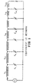
- a nonlinear transmission line is an LC ladder network, as shown in Fig. 1, in which the capacitance of capacitors C k is dependent on the voltage across them and/or the inductance of inductors L k is dependent on the current through them.
- actual implementations of nonlinear transmission lines have been constructed using varactor diodes as the voltage-variable capacitors and either discrete lumped-element inductors or lengths of transmission line as the inductors.
- T k L k ( I k ) C k ( V k )
- a varactor diode when utilized for its nonlinear properties, is ideally meant to be operated over a voltage range bounded by the punch-through voltage of the varactor diode (the maximum usable reverse-bias voltage) and the turn-on voltage of the varactor diode (the maximum usable forward-bias voltage).
- the punch-through voltage V deplete is the voltage at which there is no further change in varactor capacitance. It is assumed that the breakdown voltage is greater than or equal to V deplete .
- nonlinear transmission lines typically comprise a series of identical cells, each of which incorporates a single varactor diode having the same parametric values as the other varactor diodes in the other cells. Any portion of a pulse or step which exceeds V deplete of the varactor diode in a cell of a nonlinear transmission line will pass through that cell without being acted upon by the nonlinearity and therefore will be unchanged. This results in the inability to steepen or compress the entire step or pulse. Conversely, if the peak voltage of the propagating pulse or step is less than V deplete , then the full nonlinearity of the varactor diode is not utilized.
- Tan, et al. U.S. Pat. No. 4,855,696 discloses a unique nonperiodic cell structure for a nonlinear transmission line, which allows the propagation and compression of a single soliton.
- An interesting feature of the disclosed pulse compressor is the increase in amplitude of the soliton as it propagates from the input of the nonlinear transmission line to the output. This causes each varactor diode in the pulse compressor to experience a different voltage excursion.
- V max exceeds V deplete , the full-width-at-half-maximum (FWHM) of the output pulse is increased, the amount of uncompressed energy is increased, and the peak voltage amplitude is reduced when compared to the result if V max equals V deplete .
- V max exceeds V deplete
- the full nonlinearity of the varactor diodes is not utilized in all the other cells where the peak voltage of the propagating soliton is much less than V deplete . Accordingly, it would be desirable to provide a nonlinear transmission line which utilizes a greater range of the nonlinearity of the varactor diode in each cell and therefore produces increased pulse or step compression for a given length of nonlinear transmission line.
- low impedance sources and loads will invert the polarity of reflections.
- the inverted reflection has the proper polarity to forward bias and turn on varactor diodes in the nonlinear transmission line.
- high impedance sources and loads step up the voltage of reflections. This will generate voltages which can exceed the punch-through voltage of the varactor diodes in the nonlinear transmission line.
- the reflection both noninverted and inverted can actually pass all the way back through the nonlinear transmission line. Accordingly, it would be desirable to provide a nonlinear transmission line which optimizes power transfer by minimizing reflections due to source and load impedance mismatches.
- nonlinear transmission lines are used for edge sharpening (e.g., in samplers and step-generators) the generation of oscillatory tails is generally not welcome, since they can degrade circuit performance specifications related to flatness and stability. Accordingly, it would be desirable to provide a nonlinear transmission line in which ringing is suppressed without significantly affecting the overall risetime of the steepened edge.
- a nonlinear transmission line which utilizes varactors having noncommensurate parametric values in various cells. This results in the ability to accommodate pulses and steps which would otherwise turn on and/or greatly exceed the punch-through voltage of a series of identical single-varactor cells.
- the effective depletion voltage of selected cells increases, for example, by N .
- N 2,3, ... is the number of varactor diodes stacked in the cell
- a greater portion of the nonlinearity of the varactor diode(s) in each cell can be utilized. This results in greater pulse or step compression in a given length of nonlinear transmission line or a shorter device length for a given pulse or step compression requirement.
- oscillatory tails can be quenched without significantly affecting the overall risetime of the sharpened edge. This improves the flatness and stability of the circuit which utilizes the nonlinear transmission line.
- varactors having noncommensurate parametric values within some or all of the cells of a pulse compressor or any other nonlinear transmission line allows an additional degree of freedom for the customization and utilization in a wider variety of applications. This will become clearer in view of the following detailed description of various embodiments of the invention
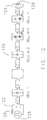
- a pulse compressor or other nonlinear transmission line is constructed utilizing specific combinations of varactor diode cells shown in Figs. 3A, 3B, 3C, and/or 3D.
- a single varactor diode cell comprises a single varactor diode V1 interconnected in a length of transmission line 3.
- a double-stacked varactor diode cell comprises two varactor diodes V1,V2 connected in series and interconnected in a length of transmission line 4.
- an N-stacked varactor diode cell comprises N varactor diodes V1, V2, ..., VN connected in series and interconnected in a length of transmission line 5.
- a "damped varactor cell” comprises a single varactor diode V1 connected in series with an extra resistance R ex interconnected in a length of transmission line 6.
- the transmission line 3, 4, 5, or 6 in a given varactor cell has a length d and an impedance Z u .
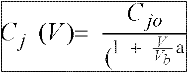
- the varactor diodes V1, V2, ..., VN are diodes which are operated in reverse bias so as to produce a voltage-dependent capacitance C j (V).
- the grading coefficient a depends on the rate at which the doping density of the varactor changes, and a > 1 for a hyperabrupt varactor.
- the capacitance per cell provided by the varactor diodes in a cell is chosen to be much larger than the capacitance of that cell introduced by the unloaded transmission line so that nonlinear capacitance of these varactors will introduce a significant nonlinearity in the capacitance per cell.
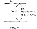
- Fig. 4 is shown an equivalent circuit of the varactor cells of Figs. 3A, 3B, 3C, and 3D.
- C j ( V ) is the voltage-dependent capacitance of the varactor diode(s) V1, V2, ..., VN, R s is the series resistance of the varactor diode(s), and L s is the inductance of the connections to the varactor diode(s).
- R ex is a separate additional resistance placed in series with a single varactor diode in the case of the varactor cell shown in Fig. 3D.
- the equivalent circuit elements determine the cutoff frequency and the propagation delay through the varactor cell.
- a varactor diode is ideally meant to be operated over a voltage range bounded by 0 ⁇
- V low is the low-voltage point and V high is the high-voltage point on the input waveform.
- V on is the turn-on voltage and V bd is the breakdown voltage of the varactor diode.
- the punch-through voltage V deplete is the voltage at which the varactor diode becomes fully depleted yielding no further change in capacitance.
- the varactor diode fabrication process technology and doping parameters of the varactor diode will set V b , C jo / C min , and a .
- the propagating pulse or step will be clipped by the varactor diodes.
- the nonlinear transmission line will begin to self-bias when conduction current flows through the varactor diodes. This will reduce the steepening ability of the nonlinear transmission line, as well as reduce the efficiency of power transfer through the nonlinear transmission line from source to load.
- Utilizing varactor diodes with larger barrier heights has only limited range, especially in the case of V on where at most V on can be increased by 50%.
- series-connecting varactor diodes has no such limitation, since both V on and V bd scale with N .
- V deplete can be decreased (refer to Eqn. (9)) by utilizing varactor diodes with larger a , utilizing varactor diodes with smaller ( C jo / C min ), and/or utilizing varactor diodes with smaller V b .
- V b has a direct effect on V on and V bd , the third alternative may not be desirable.
- Fig.5 shows a nonlinear transmission line which can propagate pulses and steps that would otherwise turn on and/or greatly exceed the punch-through voltage (or breakdown voltage) of a single varactor diode.
- a nonlinear transmission line 50 is configured such that all its m varactor cells utilize stacked varactor diodes.
- An input port 52 is connected to a pulse or step generator 54 through a source impedance 56.
- An output port 58 is connected to a load impedance 59.
- Fig. 5 shows that all varactor cells contain double-stacked varactors (Fig. 3B), which yields effective turn-on, punch-through, and breakdown voltages that are twice the turn-on, punch-through, and breakdown voltage of a single varactor.
- Fig. 3C N -stacked varactor diodes in all varactor cells yields effective turn-on, punch-through, and breakdown voltages that are N times greater than the turn-on, punch-through, and breakdown voltages of a single varactor.
- condition (8a) a particular problem occurs if only condition (8a) is exceeded but not condition (8b). That is, if
- 0.5 volt and
- 0.9 volt but
- 11 volt and
- ⁇ 11 volt it is necessary to use double-stacked varactors ( N 2) in all cells of the nonlinear transmission line to prevent turn-on.
- is now only half of the voltage necessary to fully deplete both varactors. As a result of the lower change in capacitance, a longer nonlinear transmission line will be required to achieve the required amount of steepening, which in turn results in greater insertion loss.
- the solution to this problem is to reduce V deplete by utilizing varactor diodes with larger a, utilizing varactor diodes with smaller ( C jo / C min ), and/or utilizing varactor diodes with smaller V b . If designed correctly, this more abrupt doping profile will yield the same change in capacitance across two varactor diodes as the change in capacitance across a single varactor diode using the original doping profile.
- the "3dB cutoff frequency" of the cell is that frequency ⁇ 3dB where the transfer function through the varactor cell
- has decreased by 1/ ⁇ 2 with respect to its value at ⁇ 0.
- the output transition time is related to the input transition time by Therefore, to achieve a substantial amount of steepening in as short a nonlinear transmission line as possible, the varactor diodes should dominate the transmission line characteristics, and the change in capacitance with voltage should be very large such that C j ( V 1 ) >> C j ( V 2 ) > C u .
- a nonlinear transmission line in accordance with one embodiment of the invention is shown in Fig. 6.
- a nonlinear transmission line 60 has an input port 62 and an output port 64.
- the input port 62 is connected to a pulse generator 66 through a source impedance 68.
- the output port 64 is connected to a load impedance 69.
- the nonlinear transmission line 60 is constructed of m varactor cells. Ideally, each varactor diode should be individually chosen such that the punch-through voltage V deplete of the varactor diode in each cell k is equal to the peak voltage of the soliton V peak,k in that cell.
- the compression per unit length increases as both a and C jo /C min increase (refer to Eqn.
- Varactor cells 1 through j are single-varactor cells (Fig. 3A).
- Varactor cells j +1 through k are double-stacked varactor cells (Fig. 3B).
- the peak amplitude of the soliton when it reaches varactor cell j shown in Fig. 6 is sufficient to fully deplete the single varactor diode in cell j .
- the peak amplitude of the soliton when it is in the preceding varactor cells is insufficient to fully deplete the varactor diodes in these cells.
- the peak amplitude of the soliton when it reaches varactor cell k shown in Fig. 6 is sufficient to fully deplete the double-stacked varactors in cell k .
- the peak amplitude of the soliton when it is in varactor cells j +1 through k -1 is insufficient to fully deplete the double-stacked varactor diodes in these cells.
- the peak amplitude of the soliton when it reaches varactor cell m shown in Fig. 6 is sufficient to fully deplete the triple-stacked varactors in cell m .
- the peak amplitude of the soliton when it is in varactor cells k +1 through m -1 is insufficient to fully deplete the triple-stacked varactor diodes in these cells.
- the addition of another varactor diode to a varactor cell to create a stack or increase a stack from N varactors to N +1 varactors is determined as follows. Specifically, the addition of another varactor diode occurs at the varactor diode cell where the amplitude of the propagating soliton is sufficient to fully deplete the varactor(s) in the cell if the additional varactor were not present.
- Fig. 7 shows a numerical (SPICE) simulation of the nonlinear transmission line 60 shown in Fig. 6.
- Fig. 7B shows the voltage at each varactor cell location in the nonlinear transmission line 60.
- a nonlinear transmission line in accordance with another embodiment of the invention configured to improve power transfer from source to load is shown in Fig. 8.
- a nonlinear transmission line 80 is constructed utilizing m varactor cells. Varactor cells 1 through j have a large-signal impedance Z 1, cells j +1 through k have a large-signal impedance Z 2, and cells k +1 through m have a large-signal impedance Z 3.
- An input port 82 is connected to a pulse or step generator 84 through a source impedance 86 having a value Z5 .
- An output port 88 is connected to a transmission line with impedance Z 4 > Z 5 which is in turn connected to a load impedance 89 having a value Z L .
- the double-stacked varactor diodes in cells k +1 through m are used to accommodate the step-up in voltage due to the high impedance at the output, allow the varactor diodes to be sized larger to prevent design rule violations and excessively high series resistance, reduce self-bias effects due to the inverted reflection from the low-impedance load, and absorb a greater portion of the inverted reflection from the low-impedance load, thereby reducing the level of re-reflected energy back to the load.
- the source is a 2 GHz pulse generator producing input pulses with 9 volt amplitudes and 10%-90% risetimes of 60 ps .
- the nonlinear transmission line is self-biasing (i.e., the output pulses transition between V 1 ⁇ -0.7 volt and V 2 ⁇ 9 volt ) due to the reflection from the short-circuit load.
- the large amount of ringing at the output is also be used to produce the large amount of ringing at the output.
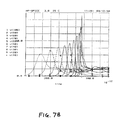
- Fig.9B shows a numerical simulation (SPICE) of the voltage at the output port 88 of a 36-cell nonlinear transmission line 80 of the form shown in Fig.8.
- the output shown in Fig. 9B shows approximately equal peak voltages as compared to the output shown in Fig. 9A. There is, however, significantly less ringing in the output shown in Fig. 9B.
- ⁇ 3dB can be decreased by decreasing ⁇ r and/or ⁇ c by utilizing a varactor diode with larger C eq and/or larger R s and/or connecting two or more varactor diodes in series.
- R stack s and/or C stack eq can be increased.
- By adding more than one varactor cell with reduced ⁇ 3dB greater damping of high-frequency ringing is accomplished.
- reducing ⁇ 3dB of a varactor cell(s) within a nonlinear transmission line comes at the expense of slowing the speed of any voltage transition that can pass through the entire device, as given by Eqn. (10).
- a "quenching shockline” comprises a nonlinear transmission line 100 having an input port 102 and an output port 104.
- the input port 102 is connected to a pulse or step generator 106 through a source impedance 108.
- the output port 104 is connected to a load impedance 109.
- the quenching shockline is constructed of m varactor cells. Cells 1 through m -2 are single-varactor cells (Fig. 3A) and the last two cells are double-stacked varactor cells (Fig. 3B).
- the stacked varactor diodes in the last two varactor cells are configured to yield a reduced change in voltage-variable capacitance C j ( V ) and larger R s (Fig. 4), resulting in a lower dynamic cutoff frequency ⁇ 3dB in these cells.
- the stacked varactor cells significantly attenuate the very high frequency harmonics generated in the previous cells, which cause the oscillatory tails (ringing).
- Fig. 11A shows a numerical (SPICE) simulation of the step response of a 40-cell nonlinear transmission line without stacked cells at its output.
- the source and load impedances are 50 ⁇ .
- the input step 110 as a 9.5 volt amplitude and a 10%-90% risetime of 55 ps .
- the output 112 is a steepened step with a 6.3 ps 10%-90% risetime but with significant ringing 114 of 1.6 volt peak-to-peak
- Fig. 11B shows a numerical (SPICE) simulation of the step response of the 40-cell nonlinear transmission line of Fig. 6 with the last two cells having double-stacked varactor diodes.
- the input step 116 shown in Fig. 11B has a 9.5 volt amplitude and a 10%-90% risetime of 55 ps .
- the output 118 is a steepened step with an 8.1 ps 10%-90% risetime which represents only a 3.7% decrease in the amount of steepening (48.7 ps for the case of Fig. 11A versus 46.9 ps for the case of Fig. 11B).
- the ringing 119 is significantly reduced to 0.1 volt peak-to-peak.
- the first approach is undesirable since capacitors are difficult to fabricate in monolithic integrated circuits.
- the middle approach increases the length of the nonlinear transmission line and is therefore undesirable.
- the last alternative requires an additional semiconductor processing step to fabricate R ex , but is achievable.
- Fig.12 is similar to Fig.10 except that the dynamic cutoff frequencies of varactor cells m -1 ad m are reduced, not by the utilization of stacked varactor diodes, but by the utilization of the extra resistance R ex in series with a single varactor (Fig.3D) in the last two varactor cells.
- Fig.13 shows a numerical (SPICE) simulation of the step response of the 40-cell nonlinear transmission line 120 shown in Fig.12 with the last two varactor cells using single varactors in series with the extra resistance R ex .
- the input step 130 shown in Fig.13 has a 9.5 volt amplitude and a 10%-90% risetime of 55 ps .
- the output 132 is a steepened step with an 8.1 ps 10%-90% risetime, but the ringing 134 is significantly reduced to 0.1 volt peak-to-peak. This is identical to the simulation shown in Fig.11B, since the cutoff frequencies for both cases are identical.
- a varactor cell with a single varactor but with an additional resistance R ex can be utilized, thereby quenching ringing.
- the disadvantage is that this requires an additional step during semiconductor processing as compared to the utilization of stacked varactor diodes.
- one or more cells of stacked varactors which have reduced cutoff frequencies can be utilized at the output end of a nonlinear transmission line to provide damping of the ringing generated by the preceding cells without significant degradation of the output edge speed.
- one or more cells of a single varactor in series with an extra resistance can be utilized at the output end of a nonlinear transmission line to provide damping of the ringing generated by the preceding cells without significant degradation of the output edge speed.
- any high-frequency ringing on the input signal can also be removed.
Landscapes
- Physics & Mathematics (AREA)
- Nonlinear Science (AREA)
- Semiconductor Integrated Circuits (AREA)
- Waveguides (AREA)
- Filters And Equalizers (AREA)
Claims (16)
- Eine nichtlineare Übertragungsleitung (60; 80; 100; 120) mit folgenden Merkmalen:einer unbelasteten Übertragungsleitung mit einem Eingang (62; 82; 102; 122) und einem Ausgang (64; 88; 104; 124);einer Einrichtung (66, 68; 84, 86; 106, 108; 126, 128) zum Injizieren am Übertragungsleitungseingang (62, 82; 102; 122) entweder eines Puls- oder eines Sprungsignals mit einem Profil, das im wesentlichen dem Profil eines stabilen Solitons am Eingang (62; 82; 102; 122) der Übertragungsleitung entspricht, derart, daß im wesentlichen nur ein einzelnes Soliton durch das Eingangssignal an dem Eingang (64; 88; 104; 124) der Übertragungsleitung erzeugt wird; undeiner Mehrzahl von Varaktorzellen, die die Übertragungsleitung an einer Mehrzahl von Positionen entlang der Übertragungsleitung belasten, wobei jede Varaktorzelle neben benachbarten Varaktorzellen angeordnet ist;wobei mindesten eine der Mehrzahl von Varaktorzellen, die eine Spannungs-veränderbare oder Spannungs-abhängige Kapazität aufweisen, sich von einer Spannungs-veränderbaren oder Spannungs-abhängigen Kapazität von mindestens einer anderen Varaktorzelle unterscheidet, derart, daß die Varaktorzellen der nichtlinearen Übertragungsleitung ungleich sind;dadurch gekennzeichnet, daßeine erste Varaktordiodeneinrichtung in der mindestens einen Varaktorzelle konfiguriert ist, derart, daß die Amplitude des sich ausbreitenden Solitons ausreichend ist, um die erste Varaktordiodeneinrichtung vollständig zu verarmen, daß dieselbe jedoch nicht ausreichend ist, um eine zweite Varaktordiodeneinrichtung in der mindestens einen anderen Varaktorzelle zu verarmen, wobei die zweite Varaktordiodeneinrichtung in der Übertragungsrichtung hinter der ersten Varaktordiodeneinrichtung positioniert ist, wobei mindestens eine der Varaktorzellen gestapelte Varaktordioden aufweist, um Varaktorzellen zu ergeben, welche die ungleichen Spannungsveränderlichen oder Spannungs-abhängigen Kapazitäten aufweisen.
- Eine nichtlineare Übertragungsleitung (60; 80; 100; 120) gemäß Anspruch 1, dadurch gekennzeichnet, daßdie erste Varaktordiodeneinrichtung mindestens eine Varaktordiode (V₁ ... VN) aufweist, und die zweite Varaktordiodeneinrichtung mindestens zwei gestapelte Varaktordioden aufweist.
- Eine nichtlineare Übertragungsleitung (60; 80; 100; 120) gemäß Anspruch 2, dadurch gekennzeichnet, daßdie Varaktordioden (V₁ ... VN) in Sperrichtung vorgespannte Varaktordioden sind.
- Eine nichtlineare Übertragungsleitung (60; 80; 100; 120) gemäß Anspruch 3, dadurch gekennzeichnet, daßdie Varaktordioden (V₁ ... VN) hyperabrupte Dioden sind.
- Eine nichtlineare Übertragungsleitung (60; 80; 100; 120) gemäß Anspruch 4, dadurch gekennzeichnet, daß die hyperabrupten Dioden folgende Kapazität aufweisen:
- Eine nichtlineare Übertragungsleitung (60; 80; 100; 120) gemäß Anspruch 1, dadurch gekennzeichnet, daßm Varaktorzellen existieren, wobei die Varaktorzellen 1 bis j Einzelvaraktorzellen sind, die Varaktorzellen j + 1 bis k doppelt-gestapelte Varaktorzellen sind, die Varaktorzellen k + 1 bis m dreifach-gestapelte Varaktorzellen sind, wobei die Spitzenamplitude des Solitons, wenn dasselbe die Varaktorzelle j erreicht, ausreichend ist, um die einzige Varaktordiode in Zelle j zu verarmen, wobei die Spitzenamplitude des Solitons, wenn sich dasselbe in den vorhergehenden Varaktorzellen befindet, jedoch nicht ausreichend ist, um die Varaktordioden in diesen Zellen vollständig zu verarmen, wobei die Spitzenamplitude des Solitons, wenn dasselbe die Varaktorzelle k erreicht, ausreichend ist, um die doppelt-gestapelten Varaktoren in der Zelle k vollständig zu verarmen, wobei die Spitzenamplitude des Solitons, wenn sich dasselbe in den Varaktorzellen j + 1 bis k - 1 befindet, jedoch nicht ausreichend ist, um die doppelt-gestapelten Varaktordioden in diesen Zellen vollständig zu verarmen, und wobei die Spitzenamplitude des Solitons, wenn dasselbe die Varaktorzelle m erreicht, ausreichend ist, um die dreifach-gestapelten Varaktoren in der Zelle m vollständig zu verarmen, wobei die Spitzenamplitude des Solitons, wenn sich dasselbe in den Varaktorzellen k + 1 bis m - 1 befindet, jedoch nicht ausreichend ist, um die dreifach-gestapelten Varaktordioden in diesen Zellen vollständig zu verarmen.
- Eine nichtlineare Übertragungsleitung (60; 80; 100; 120) gemäß Anspruch 6, dadurch gekennzeichnet, daßdie Varaktordioden (V₁ ... VN) in Sperrichtung vorgespannte Varaktordioden sind.
- Eine nichtlineare Übertragungsleitung (60; 80; 100; 120) gemäß Anspruch 7, dadurch gekennzeichnet, daßdie Varaktordioden (V₁ ... VN) hyperabrupte Dioden sind.
- Eine nichtlineare Übertragungsleitung (60; 80; 100; 120) gemäß Anspruch 8, dadurch gekennzeichnet, daßdie hyperabrupten Dioden für den Fall, bei dem alle N Varaktordioden identisch sind, folgende Kapazität aufweisen:

- Eine nichtlineare Übertragungsleitung (60; 80; 100; 120) gemäß Anspruch 1, dadurch gekennzeichnet, daßdie Kapazität pro Varaktorzelle, die durch die Varaktordiodeneinrichtung in einer Zelle geschaffen wird, derart gewählt wird, daß sie viel größer als die Kapazität der Zelle ist, die durch die unbelastete Übertragungsleitung eingeführt wird, derart, daß die nichtlineare Kapazität dieser Varaktordiodeneinrichtung eine wesentliche Nichtlinearität in die Kapazität pro Zelle einführen wird.
- Eine nichtlineare Übertragungsleitung (60; 80; 100; 120) gemäß Anspruch 5, dadurch gekennzeichnet, daßdie Varaktordioden die Übertragungsleitungscharakteristika dominieren und die Kapazitätsänderung mit der Spannung sehr groß ist, derart, daß

- Eine nichtlineare Übertragungsleitung (60; 80; 100; 120) gemäß Anspruch 2, dadurch gekennzeichnet, daßm Varaktorzellen existieren und die Varaktordiodeneinrichtung in den Zellen k + 1 bis m, welche der Varaktorzelle m vorhergehen, verwendet werden, um die Spannungs-Erhöhung aufgrund der hohen Impedanz am Ausgang (64; 88; 104; 124) aufzunehmen, wobei zugelassen ist, daß die Varaktordioden bezüglich ihrer Abmessungen größer sind, um Entwurfsregelverletzungen und übermäßig hohe Serienwiderstände zu vermeiden, um Selbst-Vorspannungseffekte aufgrund der invertierten Reflexion von einer Last mit niedriger Impedanz zu reduzieren, und um einen größeren Anteil der invertierten Reflexion von der Last mit niederer Impedanz zu absorbieren, wodurch der Pegel der zur Last zurückreflektierten Energie reduziert wird.
- Eine nichtlineare Übertragungsleitung (60; 80; 100; 120) gemäß Anspruch 12, dadurch gekennzeichnet, daßdie Ersatzimpedanz der Varaktorzelle der nichtlinearen Übertragungsleitung folgendermaßen gegeben ist,

- Eine nichtlineare Übertragungsleitung (60; 80; 100; 120) gemäß Anspruch 1, dadurch gekennzeichnet, daßdie Grenzfrequenz (ω3dB) von mindestens einer Varaktorzelle in der nichtlinearen Übertragungsleitung bezüglich der Grenzfrequenz (ω3dB) in den vorherigen Zellen niedriger ist, derart, daß ein übermäßiges Klingeln entfernt wird, ohne die Gesamtanstiegszeit der verschärften Flanke wesentlich zu beeinträchtigen, wobei die untere Grenzfrequenz die sehr hohen Frequenzharmonischen, die in den vorherigen Zellen erzeugt worden sind und das Klingeln bewirken, wesentlich gedämpft werden.
- Eine nichtlineare Übertragungsleitung (60; 80; 100; 120) gemäß Anspruch 14, dadurch gekennzeichnet, daßdie nichtlineare Übertragungsleitung aus m Varaktorzellen aufgebaut ist, wobei die Varaktorzellen 1 bis m - 2 Einzelvaraktorzellen sind und die Varaktorzellen m - 1 und m doppelt-gestapelte Varaktorzellen sind, wobei die gestapelten Varaktordioden in den Varaktorzellen m - 1 und m konfiguriert sind, um eine reduzierte Veränderung in der Spannungs-veränderbaren Kapazität Cj(V) und einen größeren Serienwiderstand Rs zu ergeben, was in einer niedrigeren dynamischen Grenzfrequenz (·3dB) in diesen Zellen resultiert, wodurch die sehr hohen Frequenzharmonischen, die in den vorigen Zellen erzeugt worden sind und das Klingeln bewirken, wesentlich gedämpft werden.
- Eine nichtlineare Übertragungsleitung (60; 80; 100; 120) gemäß Anspruch 14, dadurch gekennzeichnet, daßeine oder mehr Varaktorzellen, die eine Einzelvaraktordiode (V₁) seriell zu einem zusätzlichen Widerstand (REx) aufweisen, an dem Ausgangsende der nichtlinearen Übertragungsleitung verwendet werden, um ein Dämpfen des Klingelns, das durch die vorhergehenden Varaktorzellen erzeugt worden ist, zu schaffen, ohne die Ausgangsflankengeschwindigkeit wesentlich zu verschlechtern.
Applications Claiming Priority (2)
| Application Number | Priority Date | Filing Date | Title |
|---|---|---|---|
| US512297 | 1983-07-08 | ||
| US07/512,297 US5023574A (en) | 1990-04-17 | 1990-04-17 | Nonlinear transmission lines having noncommensurate varactor cells |
Publications (2)
| Publication Number | Publication Date |
|---|---|
| EP0453744A1 EP0453744A1 (de) | 1991-10-30 |
| EP0453744B1 true EP0453744B1 (de) | 1996-05-15 |
Family
ID=24038521
Family Applications (1)
| Application Number | Title | Priority Date | Filing Date |
|---|---|---|---|
| EP91103593A Expired - Lifetime EP0453744B1 (de) | 1990-04-17 | 1991-03-08 | Nichtlineare Übertragungsleitungen mit ungleichen Elementen aus Kapazitätsdioden |
Country Status (4)
| Country | Link |
|---|---|
| US (1) | US5023574A (de) |
| EP (1) | EP0453744B1 (de) |
| JP (1) | JP2947635B2 (de) |
| DE (1) | DE69119469T2 (de) |
Families Citing this family (31)
| Publication number | Priority date | Publication date | Assignee | Title |
|---|---|---|---|---|
| US5378939A (en) * | 1987-10-06 | 1995-01-03 | The Board Of Trustees Of The Leland Stanford Junior University | Gallium arsenide monolithically integrated sampling head using equivalent time sampling having a bandwidth greater than 100 Ghz |
| US5352994A (en) * | 1987-10-06 | 1994-10-04 | The Board Of Trustees Of The Leland Stanford Junior University | Gallium arsenide monolithically integrated nonlinear transmission line impedance transformer |
| US5256996A (en) * | 1987-10-06 | 1993-10-26 | The Board Of Trustees Of The Leland Stanford, Junior University | Integrated coplanar strip nonlinear transmission line |
| DE4121569A1 (de) * | 1991-06-29 | 1993-01-14 | Standard Elektrik Lorenz Ag | Entzerrer fuer optisch uebertragene nachrichtensignale |
| US5274271A (en) * | 1991-07-12 | 1993-12-28 | Regents Of The University Of California | Ultra-short pulse generator |
| US5422607A (en) * | 1994-02-09 | 1995-06-06 | The Regents Of The University Of California | Linear phase compressive filter |
| US5804921A (en) * | 1994-02-09 | 1998-09-08 | The Regents Of The University Of California | Soliton quenching NLTL impulse circuit with a pulse forming network at the output |
| US5495253A (en) * | 1994-11-17 | 1996-02-27 | The United States Of America As Represented By The Secretary Of The Army | Soliton rejection filter |
| US6421390B1 (en) * | 1995-12-26 | 2002-07-16 | The Regents Of The University Of California | High-speed pulse-shape generator, pulse multiplexer |
| FI103743B1 (fi) | 1997-08-27 | 1999-08-31 | Insinoeoeritoimisto Juhana Yli | Linearisointipiiri |
| US6690247B2 (en) | 1999-02-05 | 2004-02-10 | Northrop Grumman Corporation | Nonlinear transmission line waveform generator having an input voltage matched to the C/V characteristic of the transmission line |
| JP2002055125A (ja) | 2000-08-08 | 2002-02-20 | Agilent Technol Inc | 標本化回路 |
| US6826208B1 (en) * | 2000-12-06 | 2004-11-30 | At&T Corp. | Nonlinear transmission line integrated circuit |
| US7084716B2 (en) | 2001-04-10 | 2006-08-01 | Picosecond Pulse Labs | Ultrafast sampler with coaxial transition |
| US6900710B2 (en) | 2001-04-10 | 2005-05-31 | Picosecond Pulse Labs | Ultrafast sampler with non-parallel shockline |
| US7358834B1 (en) | 2002-08-29 | 2008-04-15 | Picosecond Pulse Labs | Transmission line voltage controlled nonlinear signal processors |
| GB0226394D0 (en) * | 2002-11-13 | 2007-03-28 | Bae Systems Plc | Radio frequency and microwave signals |
| WO2005093895A1 (ja) | 2004-03-29 | 2005-10-06 | Nec Corporation | データ伝送装置、データ伝送用線路及びデータ伝送方法 |
| US7193486B2 (en) * | 2005-01-19 | 2007-03-20 | Northrop Grumman Corporation | Tunable, maximum power output, frequency harmonic comb generator |
| US7348863B2 (en) * | 2005-07-06 | 2008-03-25 | Northrop Grumman Corporation | Simple time domain pulse generator |
| US7532083B2 (en) * | 2006-03-23 | 2009-05-12 | Intel Corporation | Active nonlinear transmission line |
| US7612629B2 (en) | 2006-05-26 | 2009-11-03 | Picosecond Pulse Labs | Biased nonlinear transmission line comb generators |
| US20080152351A1 (en) * | 2006-12-26 | 2008-06-26 | Hannah Eric C | Data communication using solitons |
| JP4809266B2 (ja) * | 2007-02-26 | 2011-11-09 | 富士通株式会社 | 非線形伝送線路を利用したインパルス発生器 |
| US7733194B2 (en) * | 2007-11-02 | 2010-06-08 | Northrop Grumman Space And Mission Systems Corporation | Nonlinear transmission line modulator |
| US8289067B2 (en) * | 2009-09-14 | 2012-10-16 | Luxtera Inc. | Method and system for bandwidth enhancement using hybrid inductors |
| US9281809B1 (en) | 2012-05-10 | 2016-03-08 | The United States Of America As Represented By The Secretary Of The Air Force | Nonlinear transmission line extraction systems |
| US8901714B2 (en) | 2013-03-14 | 2014-12-02 | Taiwan Semiconductor Manufacturing Co., Ltd. | Transmission line formed adjacent seal ring |
| US10320373B2 (en) | 2016-10-11 | 2019-06-11 | Eagle Harbor Technologies, Inc. | RF production using nonlinear semiconductor junction capacitance |
| US10666198B2 (en) * | 2017-05-09 | 2020-05-26 | Eagle Harbor Technologies, Inc | Efficient high power microwave generation using recirculating pulses |
| JP7359885B2 (ja) * | 2022-03-14 | 2023-10-11 | アンリツ株式会社 | 非線形伝送線路およびそれを用いたサンプリングオシロスコープ |
Family Cites Families (6)
| Publication number | Priority date | Publication date | Assignee | Title |
|---|---|---|---|---|
| US3173026A (en) * | 1961-02-20 | 1965-03-09 | Nagumo Jin-Ichi | Active pulse transmission line |
| US3882431A (en) * | 1973-08-10 | 1975-05-06 | Us Navy | Digital phase shifter |
| US3983416A (en) * | 1974-12-30 | 1976-09-28 | Sperry Rand Corporation | Short pulse sequential waveform generator |
| US4361768A (en) * | 1980-09-29 | 1982-11-30 | International Business Machines Corporation | Superconducting soliton devices |
| US4855696A (en) * | 1987-12-09 | 1989-08-08 | Hewlett-Packard | Pulse compressor |
| US4956568A (en) * | 1988-12-08 | 1990-09-11 | Hewlett-Packard Company | Monolithic sampler |
-
1990
- 1990-04-17 US US07/512,297 patent/US5023574A/en not_active Expired - Lifetime
-
1991
- 1991-03-08 DE DE69119469T patent/DE69119469T2/de not_active Expired - Fee Related
- 1991-03-08 EP EP91103593A patent/EP0453744B1/de not_active Expired - Lifetime
- 1991-04-17 JP JP3112510A patent/JP2947635B2/ja not_active Expired - Fee Related
Also Published As
| Publication number | Publication date |
|---|---|
| JP2947635B2 (ja) | 1999-09-13 |
| US5023574A (en) | 1991-06-11 |
| DE69119469D1 (de) | 1996-06-20 |
| DE69119469T2 (de) | 1996-10-02 |
| JPH04227311A (ja) | 1992-08-17 |
| EP0453744A1 (de) | 1991-10-30 |
Similar Documents
| Publication | Publication Date | Title |
|---|---|---|
| EP0453744B1 (de) | Nichtlineare Übertragungsleitungen mit ungleichen Elementen aus Kapazitätsdioden | |
| US4855696A (en) | Pulse compressor | |
| US5485118A (en) | Non-uniformly distributed power amplifier | |
| Baker | High voltage pulse generation using current mode second breakdown in a bipolar junction transistor | |
| Carman et al. | V-band and W-band broadband, monolithic distributed frequency multipliers | |
| Darling et al. | High-power pulsed RF extraction from nonlinear lumped element transmission lines | |
| Caloz et al. | Characteristics and potential applications of nonlinear left‐handed transmission lines | |
| US7671702B2 (en) | 2D transmission line-based apparatus and method | |
| KR100979155B1 (ko) | 비선형 전송 선로를 이용한 임펄스 발생기 | |
| Aguirre et al. | 50-GHz SiGe HBT distributed amplifiers employing constant-k and m-derived filter sections | |
| US7193486B2 (en) | Tunable, maximum power output, frequency harmonic comb generator | |
| US20220385276A1 (en) | Multi-pass nonlinear network for microwave generation | |
| Baker et al. | Generation of kilovolt-subnanosecond pulses using a nonlinear transmission line | |
| Raimundi et al. | RF generation at 200 MHz using a SiC Schottky diode lumped NLTL | |
| Kintis et al. | An MMIC pulse generator using dual nonlinear transmission lines | |
| Sack et al. | Blumlein-Generator with a GaN-HEMT in gate-boosted Operation as Closing Switch | |
| Darling et al. | High power pulse burst generation by soliton-type oscillation on nonlinear lumped element transmission lines | |
| US3612914A (en) | Avalanche diode circuits | |
| Toifl et al. | A 23GHz differential amplifier with monolithically integrated T-coils in 0.09/spl mu/m CMOS technology | |
| Madhushree et al. | RF pulse generation using nonlinear transmission lines | |
| US3686516A (en) | High voltage pulse generator | |
| Eltawil et al. | Low-voltage chaotic oscillator with an approximate cubic nonlinearity | |
| Heydari | Design issues in low-voltage high-speed current-mode logic buffers | |
| Neto et al. | Improving the voltage modulation depth and RF power generated on Nonlinear Transmission lines | |
| DE1591314C3 (de) | Vorrichtung zum Erzeugen und Verstärken elektrischer Hochfrequenzsignale |
Legal Events
| Date | Code | Title | Description |
|---|---|---|---|
| PUAI | Public reference made under article 153(3) epc to a published international application that has entered the european phase |
Free format text: ORIGINAL CODE: 0009012 |
|
| AK | Designated contracting states |
Kind code of ref document: A1 Designated state(s): DE FR GB |
|
| 17P | Request for examination filed |
Effective date: 19920428 |
|
| 17Q | First examination report despatched |
Effective date: 19940330 |
|
| GRAH | Despatch of communication of intention to grant a patent |
Free format text: ORIGINAL CODE: EPIDOS IGRA |
|
| GRAA | (expected) grant |
Free format text: ORIGINAL CODE: 0009210 |
|
| AK | Designated contracting states |
Kind code of ref document: B1 Designated state(s): DE FR GB |
|
| PG25 | Lapsed in a contracting state [announced via postgrant information from national office to epo] |
Ref country code: FR Effective date: 19960515 |
|
| REF | Corresponds to: |
Ref document number: 69119469 Country of ref document: DE Date of ref document: 19960620 |
|
| EN | Fr: translation not filed | ||
| PLBE | No opposition filed within time limit |
Free format text: ORIGINAL CODE: 0009261 |
|
| STAA | Information on the status of an ep patent application or granted ep patent |
Free format text: STATUS: NO OPPOSITION FILED WITHIN TIME LIMIT |
|
| 26N | No opposition filed | ||
| REG | Reference to a national code |
Ref country code: GB Ref legal event code: 732E |
|
| REG | Reference to a national code |
Ref country code: GB Ref legal event code: 732E |
|
| REG | Reference to a national code |
Ref country code: GB Ref legal event code: IF02 |
|
| PGFP | Annual fee paid to national office [announced via postgrant information from national office to epo] |
Ref country code: GB Payment date: 20060329 Year of fee payment: 16 |
|
| PGFP | Annual fee paid to national office [announced via postgrant information from national office to epo] |
Ref country code: DE Payment date: 20060502 Year of fee payment: 16 |
|
| GBPC | Gb: european patent ceased through non-payment of renewal fee |
Effective date: 20070308 |
|
| PG25 | Lapsed in a contracting state [announced via postgrant information from national office to epo] |
Ref country code: DE Free format text: LAPSE BECAUSE OF NON-PAYMENT OF DUE FEES Effective date: 20071002 |
|
| PG25 | Lapsed in a contracting state [announced via postgrant information from national office to epo] |
Ref country code: GB Free format text: LAPSE BECAUSE OF NON-PAYMENT OF DUE FEES Effective date: 20070308 |