EP0452817B1 - Semiconductor device with MOS-transistors and method of manufacturing the same - Google Patents
Semiconductor device with MOS-transistors and method of manufacturing the same Download PDFInfo
- Publication number
- EP0452817B1 EP0452817B1 EP19910105804 EP91105804A EP0452817B1 EP 0452817 B1 EP0452817 B1 EP 0452817B1 EP 19910105804 EP19910105804 EP 19910105804 EP 91105804 A EP91105804 A EP 91105804A EP 0452817 B1 EP0452817 B1 EP 0452817B1
- Authority
- EP
- European Patent Office
- Prior art keywords
- mos transistor
- source
- opening
- well layer
- channel region
- Prior art date
- Legal status (The legal status is an assumption and is not a legal conclusion. Google has not performed a legal analysis and makes no representation as to the accuracy of the status listed.)
- Expired - Lifetime
Links
- 239000004065 semiconductor Substances 0.000 title claims description 29
- 238000004519 manufacturing process Methods 0.000 title claims description 12
- 239000012535 impurity Substances 0.000 claims description 23
- 239000000758 substrate Substances 0.000 claims description 23
- 238000000034 method Methods 0.000 claims description 10
- 238000002513 implantation Methods 0.000 claims description 5
- 238000005468 ion implantation Methods 0.000 claims description 5
- 238000009792 diffusion process Methods 0.000 description 22
- 229910052698 phosphorus Inorganic materials 0.000 description 7
- 239000011574 phosphorus Substances 0.000 description 7
- OAICVXFJPJFONN-UHFFFAOYSA-N Phosphorus Chemical compound [P] OAICVXFJPJFONN-UHFFFAOYSA-N 0.000 description 5
- 230000001133 acceleration Effects 0.000 description 2
- XAGFODPZIPBFFR-UHFFFAOYSA-N aluminium Chemical compound [Al] XAGFODPZIPBFFR-UHFFFAOYSA-N 0.000 description 2
- 229910052782 aluminium Inorganic materials 0.000 description 2
- 150000002500 ions Chemical class 0.000 description 2
- -1 phosphorus ions Chemical class 0.000 description 2
- 238000007796 conventional method Methods 0.000 description 1
- 230000003247 decreasing effect Effects 0.000 description 1
- 239000007943 implant Substances 0.000 description 1
- 239000000463 material Substances 0.000 description 1
- 238000012986 modification Methods 0.000 description 1
- 230000004048 modification Effects 0.000 description 1
- 229910021420 polycrystalline silicon Inorganic materials 0.000 description 1
- 229920005591 polysilicon Polymers 0.000 description 1
- 239000001117 sulphuric acid Substances 0.000 description 1
Images


Classifications
-
- H—ELECTRICITY
- H01—ELECTRIC ELEMENTS
- H01L—SEMICONDUCTOR DEVICES NOT COVERED BY CLASS H10
- H01L29/00—Semiconductor devices adapted for rectifying, amplifying, oscillating or switching, or capacitors or resistors with at least one potential-jump barrier or surface barrier, e.g. PN junction depletion layer or carrier concentration layer; Details of semiconductor bodies or of electrodes thereof ; Multistep manufacturing processes therefor
- H01L29/66—Types of semiconductor device ; Multistep manufacturing processes therefor
- H01L29/66007—Multistep manufacturing processes
- H01L29/66075—Multistep manufacturing processes of devices having semiconductor bodies comprising group 14 or group 13/15 materials
- H01L29/66227—Multistep manufacturing processes of devices having semiconductor bodies comprising group 14 or group 13/15 materials the devices being controllable only by the electric current supplied or the electric potential applied, to an electrode which does not carry the current to be rectified, amplified or switched, e.g. three-terminal devices
- H01L29/66409—Unipolar field-effect transistors
- H01L29/66477—Unipolar field-effect transistors with an insulated gate, i.e. MISFET
- H01L29/66568—Lateral single gate silicon transistors
- H01L29/66575—Lateral single gate silicon transistors where the source and drain or source and drain extensions are self-aligned to the sides of the gate
-
- H—ELECTRICITY
- H01—ELECTRIC ELEMENTS
- H01L—SEMICONDUCTOR DEVICES NOT COVERED BY CLASS H10
- H01L21/00—Processes or apparatus adapted for the manufacture or treatment of semiconductor or solid state devices or of parts thereof
- H01L21/02—Manufacture or treatment of semiconductor devices or of parts thereof
- H01L21/04—Manufacture or treatment of semiconductor devices or of parts thereof the devices having at least one potential-jump barrier or surface barrier, e.g. PN junction, depletion layer or carrier concentration layer
- H01L21/18—Manufacture or treatment of semiconductor devices or of parts thereof the devices having at least one potential-jump barrier or surface barrier, e.g. PN junction, depletion layer or carrier concentration layer the devices having semiconductor bodies comprising elements of Group IV of the Periodic System or AIIIBV compounds with or without impurities, e.g. doping materials
- H01L21/26—Bombardment with radiation
- H01L21/263—Bombardment with radiation with high-energy radiation
- H01L21/265—Bombardment with radiation with high-energy radiation producing ion implantation
- H01L21/266—Bombardment with radiation with high-energy radiation producing ion implantation using masks
-
- H—ELECTRICITY
- H01—ELECTRIC ELEMENTS
- H01L—SEMICONDUCTOR DEVICES NOT COVERED BY CLASS H10
- H01L21/00—Processes or apparatus adapted for the manufacture or treatment of semiconductor or solid state devices or of parts thereof
- H01L21/70—Manufacture or treatment of devices consisting of a plurality of solid state components formed in or on a common substrate or of parts thereof; Manufacture of integrated circuit devices or of parts thereof
- H01L21/77—Manufacture or treatment of devices consisting of a plurality of solid state components or integrated circuits formed in, or on, a common substrate
- H01L21/78—Manufacture or treatment of devices consisting of a plurality of solid state components or integrated circuits formed in, or on, a common substrate with subsequent division of the substrate into plural individual devices
- H01L21/82—Manufacture or treatment of devices consisting of a plurality of solid state components or integrated circuits formed in, or on, a common substrate with subsequent division of the substrate into plural individual devices to produce devices, e.g. integrated circuits, each consisting of a plurality of components
- H01L21/822—Manufacture or treatment of devices consisting of a plurality of solid state components or integrated circuits formed in, or on, a common substrate with subsequent division of the substrate into plural individual devices to produce devices, e.g. integrated circuits, each consisting of a plurality of components the substrate being a semiconductor, using silicon technology
- H01L21/8232—Field-effect technology
- H01L21/8234—MIS technology, i.e. integration processes of field effect transistors of the conductor-insulator-semiconductor type
- H01L21/823437—MIS technology, i.e. integration processes of field effect transistors of the conductor-insulator-semiconductor type with a particular manufacturing method of the gate conductors, e.g. particular materials, shapes
- H01L21/823456—MIS technology, i.e. integration processes of field effect transistors of the conductor-insulator-semiconductor type with a particular manufacturing method of the gate conductors, e.g. particular materials, shapes gate conductors with different shapes, lengths or dimensions
-
- H—ELECTRICITY
- H01—ELECTRIC ELEMENTS
- H01L—SEMICONDUCTOR DEVICES NOT COVERED BY CLASS H10
- H01L29/00—Semiconductor devices adapted for rectifying, amplifying, oscillating or switching, or capacitors or resistors with at least one potential-jump barrier or surface barrier, e.g. PN junction depletion layer or carrier concentration layer; Details of semiconductor bodies or of electrodes thereof ; Multistep manufacturing processes therefor
- H01L29/02—Semiconductor bodies ; Multistep manufacturing processes therefor
- H01L29/06—Semiconductor bodies ; Multistep manufacturing processes therefor characterised by their shape; characterised by the shapes, relative sizes, or dispositions of the semiconductor regions ; characterised by the concentration or distribution of impurities within semiconductor regions
- H01L29/10—Semiconductor bodies ; Multistep manufacturing processes therefor characterised by their shape; characterised by the shapes, relative sizes, or dispositions of the semiconductor regions ; characterised by the concentration or distribution of impurities within semiconductor regions with semiconductor regions connected to an electrode not carrying current to be rectified, amplified or switched and such electrode being part of a semiconductor device which comprises three or more electrodes
- H01L29/1025—Channel region of field-effect devices
- H01L29/1029—Channel region of field-effect devices of field-effect transistors
- H01L29/1033—Channel region of field-effect devices of field-effect transistors with insulated gate, e.g. characterised by the length, the width, the geometric contour or the doping structure
- H01L29/1041—Channel region of field-effect devices of field-effect transistors with insulated gate, e.g. characterised by the length, the width, the geometric contour or the doping structure with a non-uniform doping structure in the channel region surface
- H01L29/1045—Channel region of field-effect devices of field-effect transistors with insulated gate, e.g. characterised by the length, the width, the geometric contour or the doping structure with a non-uniform doping structure in the channel region surface the doping structure being parallel to the channel length, e.g. DMOS like
Definitions
- the present invention relates to a semiconductor device and a method of manufacturing the same and, more particularly, to a semiconductor device and a method of manufacturing the same, which are suitably used when MOS transistors having different threshold voltages are to be obtained by a single step.
- the threshold voltage of a MOS transistor and, more particularly, of a D-type (Depletion) transistor is determined by the type and amount of an impurity used for the step of ion implantation in a channel, as shown in Figs. 1A to 1C.
- Fig. 1A shows a step of forming a gate insulating film 2 having a thickness of, e.g., 20nm (200 ⁇ ) on, e.g., a p-type semiconductor substrate 1.
- Fig. 1B shows a step of ion implantation in a channel for controlling the threshold voltage of a MOS transistor.
- Fig. 1A shows a step of forming a gate insulating film 2 having a thickness of, e.g., 20nm (200 ⁇ ) on, e.g., a p-type semiconductor substrate 1.
- Fig. 1B shows a step of ion implantation in a channel for controlling the threshold voltage of a MOS transistor.
- phosphorus ions 3 are implanted at an acceleration energy of 70 KeV to a concentration of about 1 ⁇ 1012 cm ⁇ 2 in order to form, e.g., a depletion-type transistor.
- Fig. 1C shows a step of forming a gate electrode 4 and source and drain diffusion layers 5. In this case, when n-type polysilicon is used as the material of the gate electrode 4, the threshold voltage of the transistor is about -2 V.
- Reference numeral 6 denotes an insulating film; and 7, an aluminum wiring layer.
- the present invention has been made in view of the above situation and has as its object to provide a semiconductor device having different threshold voltages in a plurality of MOS transistors, and a method of manufacturing the same with fewer steps than in a conventional method.
- a semiconductor device comprising a semiconductor substrate of one conductivity type, a MOS transistor formed in a surface of said semiconductor substrate and having source and drain layers of a conductivity type opposite to that of said semiconductor substrate, said MOS transistor further comprising a channel region formed under an insulated gate electrode between the source and drain regions, and a doped well layer formed in the channel region to control a threshold voltage of said MOS transistor, wherein said well layer has a substantially semicircular cross-section with respect to a plane perpendicular to said surface.
- a semiconductor device comprises a semiconductor substrate of one conductivity type, a MOS transistor, formed in the semiconductor substrate and having source and drain layers of a conductivity type opposite to that of the semiconductor substrate, and a well layer formed in the vicinity of a channel region of the MOS transistor to control a threshold voltage thereof, wherein the well layer has a substantially semi-circular section with a non-flat lower surface.
- a method of the present invention comprises the steps of forming a mask in which a mask pattern width of a portion corresponding to a mask opening diameter is equal to or less than twice the diffusion depth of a well layer, and implanting an impurity in a prospective channel portion of a MOS transistor of a semiconductor substrate by using the mask, thereby forming the well layer.
- a semiconductor device having a well formed in a semiconductor substrate by setting the width of a portion of a mask pattern, used for impurity implantation, that corresponds to an opening diameter to be equal to or less than twice the diffusion depth of a well layer, and gate electrodes formed to have the well layer as a channel region of a MOS transistor.
- the well formed in the above manner has a substantially semi-circular section to facilitate impurity concentration control in the surface of the substrate (in the conventional well, since the impurity is implanted through a portion of a mask pattern having a considerably larger width than in the present invention, the surface concentration is uniform and it is difficult to control the threshold voltage). Furthermore, since a plurality of types of opening patterns having a small mask pattern width are formed in a single mask, MOS transistors having different threshold voltages can be formed in a single process
- a method of manufacturing a semiconductor device comprising the steps of manufacturing a mask having at least one opening, forming a well layer by implanting an impurity in a prospective channel region of a MOS transistor of a semiconductor substrate through said at least one opening, diffusing said impurity to a predetermined depth into said substrate, where said at least one opening has a dimension being not greater than twice said predetermined depth, and forming source and drain regions of said MOS transistor on opposite sides of said channel region.
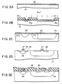
- a first thermal oxide film 22 is formed on a p-type substrate 21 having an impurity concentration of about 3 ⁇ 1015 cm ⁇ 3.
- a resist mask 23 having resist patterns of different opening widths (mask pattern widths) is formed on prospective depletion-type transistor regions, as shown in Fig. 2B.
- Phosphorus ions are implanted in the substrate 21 at a dose of about 7 ⁇ 1013 cm ⁇ 2 and an acceleration energy of 70 KeV.
- the structure is then annealed at 1,150°C for about 4 hours to diffuse the phosphorus.
- a depth X j1 of a diffusion layer 24 formed by phosphorus diffusion using a resist pattern 231 having a large width, e.g., 8 ⁇ m, is about 3 ⁇ m.
- the surface phosphorus concentration is about 3 ⁇ 1017 cm ⁇ 3.
- a depth X j2 of a well 25 formed by using a resist pattern 232 having a small width of 1 ⁇ m becomes 1 ⁇ m, and the surface concentration thereof is about 5 ⁇ 1016 cm ⁇ 3.
- MOS transistor gate electrodes 27 are formed at portions corresponding to the resist patterns 231 and 232.
- Source and drain diffusion layers 28 are formed by, e.g., ion implantation.
- an aluminum wiring layer 30 is formed over an insulating film 29 formed on the substrate as shown in Fig. 2E, thus completing MOS transistors.
- the well 24 shown in Figs. 2C to 2E is formed using the resist pattern 231 having a mask width greatly larger than twice its diffusion depth X j1 and corresponds to a conventional well.
- the well 25 is formed by using the resist pattern 232 having a mask width equal to or less than twice its diffusion depth X j2 .
- the well 25 has a substantially semi-circular section and is appropriate for threshold voltage control. This is because when a pattern opening diameter is small, the impurity concentration and the depth of a diffusion layer (especially that of an ion-implantation type) are determined by the pattern opening diameter. In this case, the length of the gate electrode on the well 25 in the channel lengthwise direction is also equal to or less than twice its well diffusion depth.
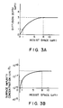
- Fig. 3A shows the resist space (opening pattern width) - diffusion depth characteristics of this embodiment
- Fig. 3B shows the resist space - diffusion layer surface impurity concentration characteristics of the same.
- the surface impurity concentration influences the threshold voltage of the MOS transistor.
- the threshold voltage can be changed in the positive direction (p-type impurity concentration is increased; n-type impurity concentration is decreased).
- the impurity concentration becomes identical to that of the p-type semiconductor substrate.
- Fig. 4A is a plan view of a pattern according to another embodiment of the present invention
- Fig. 4B is a sectional view taken along the line A - A′ of Fig. 4A.
- the same reference numerals as in Figs. 2A to 2E denote the same or identical portions in Figs. 4A to 4B.
- a plurality of mask patterns 232 for impurity implantation are arranged on the channel regions of the MOS transistors.
- the diameter of each mask pattern 232 is equal to or less than twice its diffusion depth.
- a plurality of circular resist patterns 232 are formed in the channel regions of, e.g., MOS transistors, as shown in Fig. 4A. Phosphorus is implanted in these regions, and diffusion is subsequently performed to appropriately set the surface phosphorus concentration. As a result, the threshold voltages of the MOS transistors can be set.
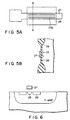
- FIG. 5A is a plan view of a pattern of this example
- Fig. 5B is a sectional view taken along the line B - B of Fig. 5A.
- two mask patterns 232 for impurity implantation are arranged parallel to the channel widthwise direction of the MOS transistors.
- the condition of the pattern width being equal to or less than twice the diffusion depth must apply only to the widthwise direction (shorter direction) of the mask patterns 232, and need not apply to the lengthwise direction.
- Fig. 6 shows still another embodiment of the present invention.
- a well 25 as shown in Fig. 6 may be adopted.
- the well 25 must similarly satisfy the above condition (the width must be equal to or less than twice the diffusion depth).
- the present invention is not limited to the above embodiments but various changes and modifications can be made.
- the shape of the mask pattern can be changed in various manners.
- the well is of a conductivity type opposite to that of the semiconductor substrate.
- the present invention can also be applied to an enhancement-type semiconductor device wherein the conductivity type of the well 25 is changed so that it will be of the same conductivity type as that of the substrate 21.
- the well has a "semi-circular" shape. However, it does not mean a true semi-circle but a shape whose bottom is not flat, unlike the well 24, but is curved, like the well 25.
- MOS transistors having different threshold voltages can be formed by the same manufacturing process (photoengraving steps) by forming a plurality of patterns having different opening diameters in a single mask, thus resulting in greatly simplified manufacturing steps.
Description
- The present invention relates to a semiconductor device and a method of manufacturing the same and, more particularly, to a semiconductor device and a method of manufacturing the same, which are suitably used when MOS transistors having different threshold voltages are to be obtained by a single step.
- Conventionally, the threshold voltage of a MOS transistor and, more particularly, of a D-type (Depletion) transistor, is determined by the type and amount of an impurity used for the step of ion implantation in a channel, as shown in Figs. 1A to 1C. Fig. 1A shows a step of forming a
gate insulating film 2 having a thickness of, e.g., 20nm (200 Å) on, e.g., a p-type semiconductor substrate 1. Fig. 1B shows a step of ion implantation in a channel for controlling the threshold voltage of a MOS transistor. In Fig. 1B,phosphorus ions 3 are implanted at an acceleration energy of 70 KeV to a concentration of about 1 × 10¹² cm⁻² in order to form, e.g., a depletion-type transistor. Fig. 1C shows a step of forming agate electrode 4 and source anddrain diffusion layers 5. In this case, when n-type polysilicon is used as the material of thegate electrode 4, the threshold voltage of the transistor is about -2V. Reference numeral 6 denotes an insulating film; and 7, an aluminum wiring layer. - In this conventional example, however, when transistors having different threshold voltages are to be formed, different types of ions must be implanted in different amounts at different places in order to set different threshold voltages. In other words, the same number of photoengraving steps as that of the required threshold voltages are required, resulting in a great increase in the number of steps. A conventional well layer is obtained by performing impurity implantation through a considerably large opening of a mask pattern (opening diameter). Therefore, the conventional well have a uniform surface impurity concentration. To form transistors having different threshold voltages in the conventional well, it is also necessary to implant different types of ions in different amounts into the different parts of the well. In this case, too, the same number of photoengraving steps as that of the threshold voltages need to be performed.
- From patent abstracts of Japan, volume 11, No. 174 (E-513) [2621-9] June 4, 1987 insulated gate FETs having different threshold voltages in the same type of well are known. The well region is formed by thermal diffusion in three dimensions, and a transistor is formed by using a region whose surface concentration is lowered.
- The present invention has been made in view of the above situation and has as its object to provide a semiconductor device having different threshold voltages in a plurality of MOS transistors, and a method of manufacturing the same with fewer steps than in a conventional method.
- This object is solved by a semiconductor device comprising a semiconductor substrate of one conductivity type, a MOS transistor formed in a surface of said semiconductor substrate and having source and drain layers of a conductivity type opposite to that of said semiconductor substrate, said MOS transistor further comprising a channel region formed under an insulated gate electrode between the source and drain regions, and a doped well layer formed in the channel region to control a threshold voltage of said MOS transistor, wherein said well layer has a substantially semicircular cross-section with respect to a plane perpendicular to said surface.
- A semiconductor device according to the present invention comprises a semiconductor substrate of one conductivity type, a MOS transistor, formed in the semiconductor substrate and having source and drain layers of a conductivity type opposite to that of the semiconductor substrate, and a well layer formed in the vicinity of a channel region of the MOS transistor to control a threshold voltage thereof, wherein the well layer has a substantially semi-circular section with a non-flat lower surface. Also, a method of the present invention comprises the steps of forming a mask in which a mask pattern width of a portion corresponding to a mask opening diameter is equal to or less than twice the diffusion depth of a well layer, and implanting an impurity in a prospective channel portion of a MOS transistor of a semiconductor substrate by using the mask, thereby forming the well layer.
- More specifically, according to the present invention, there is provided a semiconductor device having a well formed in a semiconductor substrate by setting the width of a portion of a mask pattern, used for impurity implantation, that corresponds to an opening diameter to be equal to or less than twice the diffusion depth of a well layer, and gate electrodes formed to have the well layer as a channel region of a MOS transistor. The well formed in the above manner has a substantially semi-circular section to facilitate impurity concentration control in the surface of the substrate (in the conventional well, since the impurity is implanted through a portion of a mask pattern having a considerably larger width than in the present invention, the surface concentration is uniform and it is difficult to control the threshold voltage). Furthermore, since a plurality of types of opening patterns having a small mask pattern width are formed in a single mask, MOS transistors having different threshold voltages can be formed in a single process
- Moreover, the above object is solved by a method of manufacturing a semiconductor device, comprising the steps of manufacturing a mask having at least one opening, forming a well layer by implanting an impurity in a prospective channel region of a MOS transistor of a semiconductor substrate through said at least one opening, diffusing said impurity to a predetermined depth into said substrate, where said at least one opening has a dimension being not greater than twice said predetermined depth, and forming source and drain regions of said MOS transistor on opposite sides of said channel region.
- This invention can be more fully understood from the following detailed description when taken in conjunction with the accompanying drawings, in which:
- Figs. 1A to 1C show steps of manufacturing a conventional semiconductor device;
- Figs. 2A to 2E show steps of manufacturing a semiconductor device according to an embodiment of the present invention;
- Fig. 3A is a graph of resist space - diffusion depth characteristics used for explaining the embodiment of the present invention, and Fig. 3B is a graph of resist space - surface impurity concentration characteristics used for explaining the embodiment of the present invention;
- Fig. 4A is a plan view of a pattern of another embodiment of the present invention, and Fig. 4B is a sectional view taken along the line A - A′ of Fig. 4A;
- Fig. 5A is a plan view of a pattern of still another embodiment of the present invention, and
- Fig. 5B is a sectional view taken along the line B - B of Fig. 5A; and
- Fig. 6 is a schematic sectional view of still another embodiment of the present invention.
- An embodiment of the present invention will be described with reference to Figs. 2A to 2E. First, as shown in Fig. 2A, a first
thermal oxide film 22 is formed on a p-type substrate 21 having an impurity concentration of about 3 × 10¹⁵ cm⁻³. Subsequently, aresist mask 23 having resist patterns of different opening widths (mask pattern widths) is formed on prospective depletion-type transistor regions, as shown in Fig. 2B. Phosphorus ions are implanted in thesubstrate 21 at a dose of about 7 × 10¹³ cm⁻² and an acceleration energy of 70 KeV. The structure is then annealed at 1,150°C for about 4 hours to diffuse the phosphorus. As a result, a depth Xj1 of adiffusion layer 24 formed by phosphorus diffusion using aresist pattern 23₁ having a large width, e.g., 8 µm, is about 3 µm. The surface phosphorus concentration is about 3 × 10¹⁷ cm⁻³. However, a depth Xj2 of a well 25 formed by using aresist pattern 23₂ having a small width of 1 µm becomes 1 µm, and the surface concentration thereof is about 5 × 10¹⁶ cm⁻³. - Thereafter, the
oxide film 22 is removed, and agate insulating film 26 is deposited for about 200 Å. MOStransistor gate electrodes 27 are formed at portions corresponding to theresist patterns drain diffusion layers 28 are formed by, e.g., ion implantation. Then, analuminum wiring layer 30 is formed over aninsulating film 29 formed on the substrate as shown in Fig. 2E, thus completing MOS transistors. - The well 24 shown in Figs. 2C to 2E is formed using the
resist pattern 23₁ having a mask width greatly larger than twice its diffusion depth Xj1 and corresponds to a conventional well. Thewell 25 is formed by using theresist pattern 23₂ having a mask width equal to or less than twice its diffusion depth Xj2. The well 25 has a substantially semi-circular section and is appropriate for threshold voltage control. This is because when a pattern opening diameter is small, the impurity concentration and the depth of a diffusion layer (especially that of an ion-implantation type) are determined by the pattern opening diameter. In this case, the length of the gate electrode on the well 25 in the channel lengthwise direction is also equal to or less than twice its well diffusion depth. - Fig. 3A shows the resist space (opening pattern width) - diffusion depth characteristics of this embodiment, and Fig. 3B shows the resist space - diffusion layer surface impurity concentration characteristics of the same. The surface impurity concentration influences the threshold voltage of the MOS transistor. As is apparent from Figs. 3A and 3B, when the opening pattern is set to have a width equal to or less than twice the diffusion depth, the surface impurity concentration is greatly reduced, and the diffusion depth becomes small. In other words, when the opening pattern width is set small, i.e., equal to or less than twice the diffusion depth, in the case of an n-channel MOS transistor, as in this embodiment, the threshold voltage can be changed in the positive direction (p-type impurity concentration is increased; n-type impurity concentration is decreased). When the pattern width becomes 0, the impurity concentration becomes identical to that of the p-type semiconductor substrate.
- Fig. 4A is a plan view of a pattern according to another embodiment of the present invention, and Fig. 4B is a sectional view taken along the line A - A′ of Fig. 4A. The same reference numerals as in Figs. 2A to 2E denote the same or identical portions in Figs. 4A to 4B. In this embodiment, a plurality of
mask patterns 23₂ for impurity implantation are arranged on the channel regions of the MOS transistors. In this case, the diameter of eachmask pattern 23₂ is equal to or less than twice its diffusion depth. More specifically, a plurality of circular resistpatterns 23₂ are formed in the channel regions of, e.g., MOS transistors, as shown in Fig. 4A. Phosphorus is implanted in these regions, and diffusion is subsequently performed to appropriately set the surface phosphorus concentration. As a result, the threshold voltages of the MOS transistors can be set. - Another narrow diffusion layer pattern can be arranged to be perpendicular to the channel lengthwise direction. Fig. 5A is a plan view of a pattern of this example, and Fig. 5B is a sectional view taken along the line B - B of Fig. 5A. In this embodiment, e.g., two
mask patterns 23₂ for impurity implantation are arranged parallel to the channel widthwise direction of the MOS transistors. In this case, the condition of the pattern width being equal to or less than twice the diffusion depth must apply only to the widthwise direction (shorter direction) of themask patterns 23₂, and need not apply to the lengthwise direction. - Fig. 6 shows still another embodiment of the present invention. When the threshold voltage goes more toward the plus side than the case of Figs. 2A to 2E, a well 25 as shown in Fig. 6 may be adopted. The well 25 must similarly satisfy the above condition (the width must be equal to or less than twice the diffusion depth).
- The present invention is not limited to the above embodiments but various changes and modifications can be made. For example, the shape of the mask pattern can be changed in various manners. In the above embodiments, the well is of a conductivity type opposite to that of the semiconductor substrate. However, the present invention can also be applied to an enhancement-type semiconductor device wherein the conductivity type of the well 25 is changed so that it will be of the same conductivity type as that of the
substrate 21. In the above embodiments, the well has a "semi-circular" shape. However, it does not mean a true semi-circle but a shape whose bottom is not flat, unlike the well 24, but is curved, like the well 25. - According to the present invention, MOS transistors having different threshold voltages can be formed by the same manufacturing process (photoengraving steps) by forming a plurality of patterns having different opening diameters in a single mask, thus resulting in greatly simplified manufacturing steps.
- Reference signs in the claims are intended for better understanding and shall not limit the scope.
Claims (12)
- A semiconductor device comprising a semiconductor substrate (21) of one conductivity type, a MOS transistor formed in a surface of said semiconductor substrate and having source and drain layers (28) of a conductivity type opposite to that of said semiconductor substrate, said MOS transistor further comprising a channel region formed under an insulated gate electrode (27) between the source and drain regions, and a doped well layer (25) formed in the channel region to control a threshold voltage of said MOS transistor, wherein said well layer has a substantially semicircular cross-section with respect to a plane perpendicular to said surface.
- A device according to claim 1,
characterized in that said well layer is of the same conductivity type as that of said source and drain layers of said MOS transistor. - A device according to claim 1,
characterized in that said well layer is of a conductivity type opposite to that of said source and drain layers of said MOS transistors. - A method of manufacturing a semiconductor device,
comprising the steps of manufacturing a mask (23) having at least one opening (23₂),forming a well layer (25) by implanting an impurity in a prospective channel region of a MOS transistor of a semiconductor substrate through said at least one opening, diffusing said impurity to a predetermined depth into said substrate, where said at least one opening has a dimension being not greater than twice said predetermined depth, and forming source and drain regions (28) of said MOS transistor on opposite sides of said channel region. - A method according to claim 4, further comprising the step of forming an insulated gate electrode (27) of said MOS transistor above said channel region, wherein the length of said gate electrode is not longer than twice said predetermined depth.
- A method according to claim 4,
characterized in that a single mask has a plurality of said at least one opening. - A method according to claim 6,
characterized in that the mask also includes a second opening (23₁) with its dimensions being larger than twice said predetermined depth. - A method according to claim 4, further comprising the steps of forming an insulated gate electrode (27) above said channel region, forming said source and drain regions (28) by ion implantation using said gate electrode (27) as a mask.
- A method according to claim 4,
characterized in that a plurality of said at least one opening are elongated in a direction perpendicular to the current-path in the channel region. - A method according to claim 4,
characterized in that a plurality of said at least one opening for impurity implantation are arranged on channel regions of a plurality of said MOS transistors. - A method according to claim 4,
characterized in that said well layer is of the same conductivity type as that of said source and drain layers. - A method according to claim 4,
characterized in that said well layer is of a conductivity type opposite to that of said source and drain layers.
Applications Claiming Priority (2)
| Application Number | Priority Date | Filing Date | Title |
|---|---|---|---|
| JP2104580A JP2809810B2 (en) | 1990-04-20 | 1990-04-20 | Method for manufacturing semiconductor device |
| JP104580/90 | 1990-04-20 |
Publications (2)
| Publication Number | Publication Date |
|---|---|
| EP0452817A1 EP0452817A1 (en) | 1991-10-23 |
| EP0452817B1 true EP0452817B1 (en) | 1995-10-11 |
Family
ID=14384375
Family Applications (1)
| Application Number | Title | Priority Date | Filing Date |
|---|---|---|---|
| EP19910105804 Expired - Lifetime EP0452817B1 (en) | 1990-04-20 | 1991-04-11 | Semiconductor device with MOS-transistors and method of manufacturing the same |
Country Status (4)
| Country | Link |
|---|---|
| EP (1) | EP0452817B1 (en) |
| JP (1) | JP2809810B2 (en) |
| KR (1) | KR940008357B1 (en) |
| DE (1) | DE69113673T2 (en) |
Families Citing this family (11)
| Publication number | Priority date | Publication date | Assignee | Title |
|---|---|---|---|---|
| JP3367776B2 (en) * | 1993-12-27 | 2003-01-20 | 株式会社東芝 | Semiconductor device |
| EP0915509B1 (en) * | 1997-10-24 | 2005-12-28 | STMicroelectronics S.r.l. | Process for integrating, in a same semiconductor chip, MOS technology devices with different threshold voltages |
| JP4236722B2 (en) | 1998-02-05 | 2009-03-11 | 株式会社半導体エネルギー研究所 | Method for manufacturing semiconductor device |
| JP2003007723A (en) * | 2001-06-26 | 2003-01-10 | Kitakyushu Foundation For The Advancement Of Industry Science & Technology | Semiconductor element and semiconductor integrated circuit |
| JP2004228466A (en) | 2003-01-27 | 2004-08-12 | Renesas Technology Corp | Integrated semiconductor device and manufacturing method therefor |
| JP4896699B2 (en) * | 2006-12-21 | 2012-03-14 | 株式会社半導体エネルギー研究所 | Insulated gate type semiconductor device and manufacturing method thereof |
| JP4628399B2 (en) * | 2007-06-05 | 2011-02-09 | 株式会社半導体エネルギー研究所 | Semiconductor device |
| CN113363324B (en) * | 2020-03-05 | 2024-01-30 | 上海积塔半导体有限公司 | P-channel planar VDMOS and planar IGBT |
| CN113363308B (en) * | 2020-03-05 | 2024-03-15 | 上海积塔半导体有限公司 | P-channel trench VDMOS and trench IGBT |
| CN113363322B (en) * | 2020-03-05 | 2023-12-08 | 上海积塔半导体有限公司 | N-channel trench VDMOS and trench IGBT |
| CN113363318B (en) * | 2020-03-05 | 2023-12-08 | 上海积塔半导体有限公司 | N-channel planar VDMOS and planar IGBT |
Family Cites Families (2)
| Publication number | Priority date | Publication date | Assignee | Title |
|---|---|---|---|---|
| JPS5120916B2 (en) * | 1973-04-11 | 1976-06-29 | ||
| JPS52127181A (en) * | 1976-04-19 | 1977-10-25 | Nippon Telegr & Teleph Corp <Ntt> | Insulated gate type filed effect transistor |
-
1990
- 1990-04-20 JP JP2104580A patent/JP2809810B2/en not_active Expired - Fee Related
-
1991
- 1991-04-11 DE DE1991613673 patent/DE69113673T2/en not_active Expired - Fee Related
- 1991-04-11 EP EP19910105804 patent/EP0452817B1/en not_active Expired - Lifetime
- 1991-04-16 KR KR1019910006071A patent/KR940008357B1/en not_active IP Right Cessation
Also Published As
| Publication number | Publication date |
|---|---|
| EP0452817A1 (en) | 1991-10-23 |
| KR940008357B1 (en) | 1994-09-12 |
| DE69113673D1 (en) | 1995-11-16 |
| JPH043468A (en) | 1992-01-08 |
| JP2809810B2 (en) | 1998-10-15 |
| DE69113673T2 (en) | 1996-04-18 |
Similar Documents
| Publication | Publication Date | Title |
|---|---|---|
| US5210437A (en) | MOS device having a well layer for controlling threshold voltage | |
| US5548143A (en) | Metal oxide semiconductor transistor and a method for manufacturing the same | |
| US6147383A (en) | LDD buried channel field effect semiconductor device and manufacturing method | |
| EP0164449B1 (en) | Process for producing a semiconductor integrated circuit device including a misfet | |
| KR950002276B1 (en) | Process for producing cmos having doped polysilicon gate by outdiffusion of boron from implanted silicide gate | |
| KR0137625B1 (en) | Structure and manufacture of semiconductor | |
| US6879006B2 (en) | MOS transistor and method for fabricating the same | |
| US5917218A (en) | Peripheral circuits including high voltage transistors with LDD structures for nonvolatile memories | |
| US4637128A (en) | Method of producing semiconductor device | |
| EP0452817B1 (en) | Semiconductor device with MOS-transistors and method of manufacturing the same | |
| US5212542A (en) | Semiconductor device having at least two field effect transistors and method of manufacturing the same | |
| EP0683531B1 (en) | MOSFET with LDD structure and manufacturing method therefor | |
| JPH08213479A (en) | Manufacture of mis transistor and semiconductor device | |
| US6713331B2 (en) | Semiconductor device manufacturing using one element separation film | |
| US20050037581A1 (en) | Multibit ROM cell and method therefor | |
| KR100556350B1 (en) | Semiconductor device and fabricating Method for the same | |
| KR0166991B1 (en) | Method of manufacturing a semiconductor device provided with an isolation region | |
| KR100311498B1 (en) | Method for forming dual gate of semiconductor device | |
| JPH09223797A (en) | Manufacture of semiconductor device | |
| EP0421446B1 (en) | Semiconductor device wherein n-channel MOSFET, p-channel MOSFET and nonvolatile memory cell are formed in one chip | |
| KR100431324B1 (en) | Manufacturing Method of Semiconductor Device | |
| KR940005291B1 (en) | Manufacturing method of semiconductor device using an impurity segregation phenomenon | |
| JPS62265765A (en) | Semiconductor device and manufacture thereof | |
| JP2595058B2 (en) | Manufacturing method of nonvolatile semiconductor memory device | |
| KR100252747B1 (en) | Flash memory device and manufacturing method thereof |
Legal Events
| Date | Code | Title | Description |
|---|---|---|---|
| PUAI | Public reference made under article 153(3) epc to a published international application that has entered the european phase |
Free format text: ORIGINAL CODE: 0009012 |
|
| 17P | Request for examination filed |
Effective date: 19910411 |
|
| AK | Designated contracting states |
Kind code of ref document: A1 Designated state(s): DE FR GB |
|
| 17Q | First examination report despatched |
Effective date: 19940325 |
|
| GRAA | (expected) grant |
Free format text: ORIGINAL CODE: 0009210 |
|
| AK | Designated contracting states |
Kind code of ref document: B1 Designated state(s): DE FR GB |
|
| REF | Corresponds to: |
Ref document number: 69113673 Country of ref document: DE Date of ref document: 19951116 |
|
| ET | Fr: translation filed | ||
| PLBE | No opposition filed within time limit |
Free format text: ORIGINAL CODE: 0009261 |
|
| STAA | Information on the status of an ep patent application or granted ep patent |
Free format text: STATUS: NO OPPOSITION FILED WITHIN TIME LIMIT |
|
| 26N | No opposition filed | ||
| PGFP | Annual fee paid to national office [announced via postgrant information from national office to epo] |
Ref country code: FR Payment date: 19970409 Year of fee payment: 7 |
|
| PGFP | Annual fee paid to national office [announced via postgrant information from national office to epo] |
Ref country code: DE Payment date: 19970418 Year of fee payment: 7 |
|
| K1C1 | Correction of patent application (title page) published |
Effective date: 19911023 |
|
| PG25 | Lapsed in a contracting state [announced via postgrant information from national office to epo] |
Ref country code: FR Free format text: THE PATENT HAS BEEN ANNULLED BY A DECISION OF A NATIONAL AUTHORITY Effective date: 19980430 |
|
| REG | Reference to a national code |
Ref country code: GB Ref legal event code: 746 Effective date: 19981010 |
|
| PG25 | Lapsed in a contracting state [announced via postgrant information from national office to epo] |
Ref country code: DE Free format text: LAPSE BECAUSE OF NON-PAYMENT OF DUE FEES Effective date: 19990202 |
|
| REG | Reference to a national code |
Ref country code: FR Ref legal event code: ST |
|
| REG | Reference to a national code |
Ref country code: GB Ref legal event code: IF02 |
|
| PGFP | Annual fee paid to national office [announced via postgrant information from national office to epo] |
Ref country code: GB Payment date: 20060405 Year of fee payment: 16 |
|
| GBPC | Gb: european patent ceased through non-payment of renewal fee |
Effective date: 20070411 |
|
| PG25 | Lapsed in a contracting state [announced via postgrant information from national office to epo] |
Ref country code: GB Free format text: LAPSE BECAUSE OF NON-PAYMENT OF DUE FEES Effective date: 20070411 |