EP0452634A1 - Lead frame for semiconductor device - Google Patents
Lead frame for semiconductor device Download PDFInfo
- Publication number
- EP0452634A1 EP0452634A1 EP91102764A EP91102764A EP0452634A1 EP 0452634 A1 EP0452634 A1 EP 0452634A1 EP 91102764 A EP91102764 A EP 91102764A EP 91102764 A EP91102764 A EP 91102764A EP 0452634 A1 EP0452634 A1 EP 0452634A1
- Authority
- EP
- European Patent Office
- Prior art keywords
- lead frame
- frame
- portions
- support portion
- substrate
- Prior art date
- Legal status (The legal status is an assumption and is not a legal conclusion. Google has not performed a legal analysis and makes no representation as to the accuracy of the status listed.)
- Granted
Links
Images


Classifications
-
- H—ELECTRICITY
- H01—ELECTRIC ELEMENTS
- H01L—SEMICONDUCTOR DEVICES NOT COVERED BY CLASS H10
- H01L23/00—Details of semiconductor or other solid state devices
- H01L23/48—Arrangements for conducting electric current to or from the solid state body in operation, e.g. leads, terminal arrangements ; Selection of materials therefor
-
- G—PHYSICS
- G02—OPTICS
- G02B—OPTICAL ELEMENTS, SYSTEMS OR APPARATUS
- G02B6/00—Light guides; Structural details of arrangements comprising light guides and other optical elements, e.g. couplings
- G02B6/24—Coupling light guides
- G02B6/42—Coupling light guides with opto-electronic elements
- G02B6/4201—Packages, e.g. shape, construction, internal or external details
- G02B6/4251—Sealed packages
- G02B6/4253—Sealed packages by embedding housing components in an adhesive or a polymer material
-
- G—PHYSICS
- G02—OPTICS
- G02B—OPTICAL ELEMENTS, SYSTEMS OR APPARATUS
- G02B6/00—Light guides; Structural details of arrangements comprising light guides and other optical elements, e.g. couplings
- G02B6/24—Coupling light guides
- G02B6/42—Coupling light guides with opto-electronic elements
- G02B6/4201—Packages, e.g. shape, construction, internal or external details
- G02B6/4255—Moulded or casted packages
-
- H—ELECTRICITY
- H01—ELECTRIC ELEMENTS
- H01L—SEMICONDUCTOR DEVICES NOT COVERED BY CLASS H10
- H01L23/00—Details of semiconductor or other solid state devices
- H01L23/48—Arrangements for conducting electric current to or from the solid state body in operation, e.g. leads, terminal arrangements ; Selection of materials therefor
- H01L23/488—Arrangements for conducting electric current to or from the solid state body in operation, e.g. leads, terminal arrangements ; Selection of materials therefor consisting of soldered or bonded constructions
- H01L23/495—Lead-frames or other flat leads
- H01L23/49541—Geometry of the lead-frame
- H01L23/49544—Deformation absorbing parts in the lead frame plane, e.g. meanderline shape
-
- G—PHYSICS
- G02—OPTICS
- G02B—OPTICAL ELEMENTS, SYSTEMS OR APPARATUS
- G02B6/00—Light guides; Structural details of arrangements comprising light guides and other optical elements, e.g. couplings
- G02B6/24—Coupling light guides
- G02B6/42—Coupling light guides with opto-electronic elements
- G02B6/4201—Packages, e.g. shape, construction, internal or external details
- G02B6/4246—Bidirectionally operating package structures
-
- H—ELECTRICITY
- H01—ELECTRIC ELEMENTS
- H01L—SEMICONDUCTOR DEVICES NOT COVERED BY CLASS H10
- H01L2924/00—Indexing scheme for arrangements or methods for connecting or disconnecting semiconductor or solid-state bodies as covered by H01L24/00
- H01L2924/0001—Technical content checked by a classifier
- H01L2924/0002—Not covered by any one of groups H01L24/00, H01L24/00 and H01L2224/00
Definitions
- the present invention relates to a lead frame used, for example, as a component for producing a multi-core optical module.
- a multi-core optical module in which a plurality of optical operation elements (laser-diodes, photo diodes, etc.) are linked to a number of optical fibers, is used for building an optical communication system such as an optical local area network (LAN).
- LAN optical local area network
- a multi-core optical module electronic circuit elements are mounted on a substrate portion 1a of a lead frame (Fig. 1 or 2) and optical connectors fixing optical operation elements are connected to the substrate portion through wires. Subsequently, the lead frame is attached to a mold die, after which the multi-core optical module is produced by filling the mold die with resin.
- the optical operation elements including optical transmission circuits and optical receiving circuits are mounted on the single substrate portion 1a of the conventional lead fram 1 as shown in Fig. 1, signals of the optical transmission circuits may flow into the optical receiving circuits (cross talk) since they have a common ground, so that erroneous operations are apt to occur.
- the substrate portion 1a has an unnecessarily large area, so that a thermal stress at and after the molding step may cause deterioration by cracks generated in a formed resin portion.
- the substrate portion 1a is divided into two parts as in the conventional lead frame 1 as shown in Fig. 2, each being supported by three portions to electrically insulate the circuits, the substrate portion 1a is apt to move before the molding step, so that wires connecting the optical operation element to the substrate portion 1a are apt to be damaged. Further, the substrate portion 1a is apt to vibrate due to an ultrasonic applied at the wire bonding, so that it is difficult to assure a sufficient strength of wire bonding.
- an object of the present invention is to provide a lead frame in which a plurality of substrate portions are sufficiently fixed and are sufficiently insulated from each other in a final product.
- a lead frame including a frame portion, a plurality of substrate portions on which electronic circuit elements are to be mounted, and a support portion for supporting the plurality of substrate portions to the frame portion, the support portion having a plurality of separated end portions connected to the respective substrate portions at the position where a molded resin member is covered, and at least two of the plurality of end portions being combined into one body to be connected to the frame portion at the position where the molded resin member is not covered.
- the substrate portions are sufficiently fixed to the frame portion. Further, since the support portion has the separated end portions at the position where the molded resin member is covered, the plurality of substrate portions are insulated from each other by cutting the end portions after resin molding.
- Fig. 3 shows a lead frame according to a first embodiment of the present invention.
- a lead frame 5 includes a support portion 5c disposed between a frame portion 5b and substrate portions 5a, and lead pins 5d.
- the lead frame is attached to a mold die at resin molding, and a resin is filled into a cavity of the mold die so that a package portion is formed.
- the support portion 5c has two separated end portions inside the resin package portion P so as to support the respective substrate portions 5a and the lead pins 5d to the frame portion 5b.
- the separated end portions are combined into one body outside the package portion P to be connected to the frame portion 5b. Accordingly, the substrate portions 5a are sufficiently fixed to the frame portion 5b and the substrate portions are sufficiently insulated from each other by cutting the separated end portions after the resin molding.
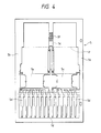
- FIG. 4 shows a second embodiment of the present invention.
- the second embodiment is equivalent to the first embodiment except that the support portion 5c has a stress absorbing portion 5f which is a thin zigzag portion provided in the support portion 5c.
- the stress absorbing portion 5f will readily deform under applied stress. Thus, even if the support portion 5c becomes shorter due to the contraction of resin after resin molding, the stress absorbing portion 5f will stretch to compensate, relieving the frame portion 5b from undesired stress. Since the frame portion 5b is no longer pushed, the lead pins 5d are no longer forced out of the inside of the formed resin. There is no clearance at the interface between the lead pins 5d and the formed resin portion, and consequently, humidity resistance and pull-out strength of the lead pins 5d are not diminished. Because no substantial stress is applied to the inner portion of the lead pins, wires bonded to the lead pin 5d are safe from breaking. Further, when unnecessary portions of the lead frame in a final product are cut off by a stamping die, it is possible to cut the portions at an accurate position, because there is no deformation of the frame portion caused by the undesired stress.
- FIG. 5 shows a third embodiment of the present invention.
- This embodiment is equivalent to the second embodimet except that stress absorbing portions 15f are disposed on a frame portion 5b.
- the stress absorbing portions 15f will contract to compensate, releiving the frame portion 5b from undesired stress.
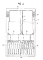
- FIG. 6 shows a lead frame according to the fourth embodiment of the present invention.
- This embodiment is equivalent to the third embodiment shown in FIG. 5 except that the separated support portion is combined into one body at the frame portion.
- This embodiment has also the same effects as those in the second embodiment.
- a resin may enter into portion A between the separated portions of support portion at the molding step, so that burrs are formed. However, this burrs can be removed at a subsequent step.
- FIG. 7 shows a lead frame according to the fifth embodiment of the present invention.
- This embodiment is equivalent to the second embodiment shown in FIG. 4 except that three substrate portions 5a and two support portions 5c are provided.
- This embodiment has also the same effects as those in the former embodiments. That is, the present invention is also applicable to a multi-core optical module having more than three cores.
Abstract
Description
- The present invention relates to a lead frame used, for example, as a component for producing a multi-core optical module.
- A multi-core optical module, in which a plurality of optical operation elements (laser-diodes, photo diodes, etc.) are linked to a number of optical fibers, is used for building an optical communication system such as an optical local area network (LAN).
- To produce such a multi-core optical module, electronic circuit elements are mounted on a
substrate portion 1a of a lead frame (Fig. 1 or 2) and optical connectors fixing optical operation elements are connected to the substrate portion through wires. Subsequently, the lead frame is attached to a mold die, after which the multi-core optical module is produced by filling the mold die with resin. - However, when the optical operation elements including optical transmission circuits and optical receiving circuits are mounted on the
single substrate portion 1a of theconventional lead fram 1 as shown in Fig. 1, signals of the optical transmission circuits may flow into the optical receiving circuits (cross talk) since they have a common ground, so that erroneous operations are apt to occur. Further, thesubstrate portion 1a has an unnecessarily large area, so that a thermal stress at and after the molding step may cause deterioration by cracks generated in a formed resin portion. - On the other hand, when the
substrate portion 1a is divided into two parts as in theconventional lead frame 1 as shown in Fig. 2, each being supported by three portions to electrically insulate the circuits, thesubstrate portion 1a is apt to move before the molding step, so that wires connecting the optical operation element to thesubstrate portion 1a are apt to be damaged. Further, thesubstrate portion 1a is apt to vibrate due to an ultrasonic applied at the wire bonding, so that it is difficult to assure a sufficient strength of wire bonding. - Therefore, an object of the present invention is to provide a lead frame in which a plurality of substrate portions are sufficiently fixed and are sufficiently insulated from each other in a final product.
- This object is accomplished by providing a lead frame including a frame portion, a plurality of substrate portions on which electronic circuit elements are to be mounted, and a support portion for supporting the plurality of substrate portions to the frame portion, the support portion having a plurality of separated end portions connected to the respective substrate portions at the position where a molded resin member is covered, and at least two of the plurality of end portions being combined into one body to be connected to the frame portion at the position where the molded resin member is not covered.
- According to the lead frame of the present invention, since the respective substrate portions are connected to the support portion, the substrate portions are sufficiently fixed to the frame portion. Further, since the support portion has the separated end portions at the position where the molded resin member is covered, the plurality of substrate portions are insulated from each other by cutting the end portions after resin molding.
-
- FIGs. 1 and 2 illustrate lead frames of prior art;
- FIG. 3 shows the first embodiment of a lead frame according to the present invention; and
- FIGs. 4 to 7 show lead frams according to the second, third, fourth and fifth embodiments of the present invention, respectively.
- Preferred embodiments of the present invention will be described with reference to the accompanying drawings.
- Fig. 3 shows a lead frame according to a first embodiment of the present invention. In Fig. 3, a
lead frame 5 includes asupport portion 5c disposed between aframe portion 5b andsubstrate portions 5a, andlead pins 5d. The lead frame is attached to a mold die at resin molding, and a resin is filled into a cavity of the mold die so that a package portion is formed. A dotted line in the figure schematically shows the package portion P formed integrally by the resin molding. Thesupport portion 5c has two separated end portions inside the resin package portion P so as to support therespective substrate portions 5a and thelead pins 5d to theframe portion 5b. The separated end portions are combined into one body outside the package portion P to be connected to theframe portion 5b. Accordingly, thesubstrate portions 5a are sufficiently fixed to theframe portion 5b and the substrate portions are sufficiently insulated from each other by cutting the separated end portions after the resin molding. - When the above lead frame is used to form a multi-core optical module, electronic circuit elements are mounted on the
substrate portions 5a and are connected to thelead pins 5d and to optical operation elements fixed to optical connectors. Then the lead frame is subjected to the resin molding to form the multi-core optical module. - FIG. 4 shows a second embodiment of the present invention. The second embodiment is equivalent to the first embodiment except that the
support portion 5c has astress absorbing portion 5f which is a thin zigzag portion provided in thesupport portion 5c. - The
stress absorbing portion 5f will readily deform under applied stress. Thus, even if thesupport portion 5c becomes shorter due to the contraction of resin after resin molding, thestress absorbing portion 5f will stretch to compensate, relieving theframe portion 5b from undesired stress. Since theframe portion 5b is no longer pushed, thelead pins 5d are no longer forced out of the inside of the formed resin. There is no clearance at the interface between thelead pins 5d and the formed resin portion, and consequently, humidity resistance and pull-out strength of thelead pins 5d are not diminished. Because no substantial stress is applied to the inner portion of the lead pins, wires bonded to thelead pin 5d are safe from breaking. Further, when unnecessary portions of the lead frame in a final product are cut off by a stamping die, it is possible to cut the portions at an accurate position, because there is no deformation of the frame portion caused by the undesired stress. - FIG. 5 shows a third embodiment of the present invention. This embodiment is equivalent to the second embodimet except that
stress absorbing portions 15f are disposed on aframe portion 5b. In this embodiment, when thesupport portion 5c becomes shorter due to the contraction of resin after resin molding, thestress absorbing portions 15f will contract to compensate, releiving theframe portion 5b from undesired stress. - FIG. 6 shows a lead frame according to the fourth embodiment of the present invention. This embodiment is equivalent to the third embodiment shown in FIG. 5 except that the separated support portion is combined into one body at the frame portion. This embodiment has also the same effects as those in the second embodiment. In this case, a resin may enter into portion A between the separated portions of support portion at the molding step, so that burrs are formed. However, this burrs can be removed at a subsequent step.
- FIG. 7 shows a lead frame according to the fifth embodiment of the present invention. This embodiment is equivalent to the second embodiment shown in FIG. 4 except that three
substrate portions 5a and twosupport portions 5c are provided. This embodiment has also the same effects as those in the former embodiments. That is, the present invention is also applicable to a multi-core optical module having more than three cores. - It will be readily apparent to those skilled in the art that other embodiments of the present invention may be implemented without departing from the scope of inventive concept expressed by the following claims.
Claims (4)
- A lead frame, comprising:
a frame portion;
a plurality of substrate portions on which electronic circuit elements are to be mounted; and
at least one support portion for supporting said plurality of substrate portions to said frame portion, said support portion having a plurality of separated end portions connected to said respective substrate portions and at least two of said plurality of end portions being combined into one body to be connected to said frame portion. - A lead frame as claimed in claim 1, wherein a stress absorbing portion is disposed in said support portion.
- A lead frame as claimed in claim 1, wherein at least one stress absorbing portion is disposed in said frame portion.
- A lead frame as claimed in claim 1, wherein said lead frame is used as a component for producing a multi-core optical module including a plurality of optical connectors fixing optical operation elements and electronic circuit elements connected to said optical operation elements.
Applications Claiming Priority (2)
| Application Number | Priority Date | Filing Date | Title |
|---|---|---|---|
| JP6617990 | 1990-03-16 | ||
| JP66179/90 | 1990-03-16 |
Publications (2)
| Publication Number | Publication Date |
|---|---|
| EP0452634A1 true EP0452634A1 (en) | 1991-10-23 |
| EP0452634B1 EP0452634B1 (en) | 1997-05-02 |
Family
ID=13308363
Family Applications (1)
| Application Number | Title | Priority Date | Filing Date |
|---|---|---|---|
| EP91102764A Expired - Lifetime EP0452634B1 (en) | 1990-03-16 | 1991-02-25 | Lead frame for semiconductor device |
Country Status (6)
| Country | Link |
|---|---|
| US (1) | US5304818A (en) |
| EP (1) | EP0452634B1 (en) |
| KR (1) | KR100208301B1 (en) |
| AU (1) | AU639764B2 (en) |
| CA (1) | CA2037006A1 (en) |
| DE (1) | DE69125884T2 (en) |
Cited By (3)
| Publication number | Priority date | Publication date | Assignee | Title |
|---|---|---|---|---|
| EP0792521B1 (en) * | 1994-10-19 | 2001-02-07 | Telefonaktiebolaget Lm Ericsson | Method for encapsulating an optocompnent using a leadframe adapted therefore |
| WO2004012485A2 (en) * | 2002-07-31 | 2004-02-05 | Freescale Semiconductor, Inc. | Mounting surfaces for electronic devices |
| US7012324B2 (en) | 2003-09-12 | 2006-03-14 | Freescale Semiconductor, Inc. | Lead frame with flag support structure |
Families Citing this family (6)
| Publication number | Priority date | Publication date | Assignee | Title |
|---|---|---|---|---|
| JPH0653394A (en) * | 1992-07-28 | 1994-02-25 | Shinko Electric Ind Co Ltd | Plane support for multilayer lead frame |
| US5854094A (en) * | 1992-07-28 | 1998-12-29 | Shinko Electric Industries Co., Ltd. | Process for manufacturing metal plane support for multi-layer lead frames |
| US5416871A (en) * | 1993-04-09 | 1995-05-16 | Sumitomo Electric Industries, Ltd. | Molded optical connector module |
| JP4161399B2 (en) * | 1998-03-12 | 2008-10-08 | 沖電気工業株式会社 | Resin substrate for semiconductor device and semiconductor device |
| EP1154240A3 (en) * | 2000-05-13 | 2003-08-20 | AB Elektronik GmbH | Angular position sensor |
| DE10128756A1 (en) * | 2001-06-13 | 2002-12-19 | Bosch Gmbh Robert | Packaging for an electronic component |
Family Cites Families (26)
| Publication number | Priority date | Publication date | Assignee | Title |
|---|---|---|---|---|
| US4149072A (en) * | 1977-08-05 | 1979-04-10 | Minnesota Mining And Manufacturing Company | System for flat ribbon optical fiber data communications link |
| US4188708A (en) * | 1977-10-03 | 1980-02-19 | National Semiconductor Corporation | Integrated circuit package with optical input coupler |
| US4136357A (en) * | 1977-10-03 | 1979-01-23 | National Semiconductor Corporation | Integrated circuit package with optical input coupler |
| JPS584952A (en) * | 1981-07-01 | 1983-01-12 | Toshiba Corp | Semiconductor device |
| EP0092330B1 (en) * | 1982-04-19 | 1990-01-10 | The Secretary of State for Defence in Her Britannic Majesty's Government of the United Kingdom of Great Britain and | Infra red photo detector systems |
| GB2126795B (en) * | 1982-09-09 | 1986-12-03 | Plessey Co Plc | Optical device |
| JPS59119774A (en) * | 1982-12-25 | 1984-07-11 | Toshiba Corp | Photo coupling semiconductor device |
| JPS59205775A (en) * | 1983-05-10 | 1984-11-21 | Sumitomo Electric Ind Ltd | Optical module |
| JPS6017411A (en) * | 1983-07-11 | 1985-01-29 | Sumitomo Electric Ind Ltd | Optical module |
| IT1169922B (en) * | 1983-11-04 | 1987-06-03 | Telettra Lab Telefon | SYSTEM AND DEVICES FOR CONNECTING DETECTORS AND FIBER OPTICS |
| FR2562271B1 (en) * | 1984-03-29 | 1986-07-18 | Telecommunications Sa | CONNECTOR OF AN OPTICAL FIBER AND A PHOTO-ELEMENT, RECEIVER OR TRANSMITTER, AND POSITIONING METHOD THEREOF |
| US4730198A (en) * | 1984-11-26 | 1988-03-08 | American Telephone And Telegraph Company, At&T Bell Laboratories | Aligning arrays of optoelectronic devices to arrays of optical fibers |
| US4803361A (en) * | 1986-05-26 | 1989-02-07 | Hitachi, Ltd. | Photoelectric device with optical fiber and laser emitting chip |
| JPS6315454A (en) * | 1986-07-08 | 1988-01-22 | Fujitsu Ltd | Lead frame semiconductor device |
| US4827118A (en) * | 1986-07-10 | 1989-05-02 | Minolta Camera Kabushiki Kaisha | Light-sensitive device having color filter and manufacturing method thereof |
| JPS62169334A (en) * | 1986-12-24 | 1987-07-25 | Hitachi Ltd | Assembling method of semiconductor device |
| EP0273364B1 (en) * | 1986-12-26 | 1992-03-25 | Idec Izumi Corporation | Electronic part carrying strip and method of manufacturing the same |
| US4820013A (en) * | 1987-01-06 | 1989-04-11 | Alps Electric Co., Ltd. | LED array head |
| JPH0719898B2 (en) * | 1987-01-30 | 1995-03-06 | 日本電気株式会社 | Optoelectronic integrated circuit |
| GB8714396D0 (en) * | 1987-06-19 | 1987-07-22 | Amp Holland | Fiber optic connector |
| JPH073907B2 (en) * | 1987-07-03 | 1995-01-18 | 株式会社日立製作所 | Dual in-line package type semiconductor laser module |
| JPH0828455B2 (en) * | 1988-02-24 | 1996-03-21 | 富士通株式会社 | Lead frame and method for manufacturing electronic component using the same |
| GB8816603D0 (en) * | 1988-07-13 | 1988-08-17 | Bt & D Technologies Ltd | Optical components |
| JP2778054B2 (en) * | 1988-10-27 | 1998-07-23 | 日本電気株式会社 | Resin-sealed photo interrupter |
| US5011256A (en) * | 1988-10-28 | 1991-04-30 | E. I. Du Pont De Nemours And Company | Package for an opto-electronic component |
| US4961107A (en) * | 1989-04-03 | 1990-10-02 | Motorola Inc. | Electrically isolated heatsink for single-in-line package |
-
1991
- 1991-02-25 DE DE69125884T patent/DE69125884T2/en not_active Expired - Lifetime
- 1991-02-25 CA CA002037006A patent/CA2037006A1/en not_active Abandoned
- 1991-02-25 EP EP91102764A patent/EP0452634B1/en not_active Expired - Lifetime
- 1991-03-08 KR KR1019910003723A patent/KR100208301B1/en not_active IP Right Cessation
- 1991-03-14 AU AU73565/91A patent/AU639764B2/en not_active Ceased
-
1992
- 1992-07-24 US US07/917,747 patent/US5304818A/en not_active Expired - Lifetime
Non-Patent Citations (3)
| Title |
|---|
| PATENT ABSTRACTS OF JAPAN vol. 009, no. 133 (P-362) 08 June 1985, & JP-A-60 017411 (SUMITOMO DENKI KOGYO KK.) 29 January 1985, * |
| PATENT ABSTRACTS OF JAPAN vol. 012, no. 009 (E-572) 12 January 1988, & JP-A-62 169334 (HITACHI LTD.) 25 July 1987, * |
| PATENT ABSTRACTS OF JAPAN vol. 012, no. 221 (E-625) 23 June 1988, & JP-A-63 015454 (FUJITSU LTD.) 22 January 1988, * |
Cited By (6)
| Publication number | Priority date | Publication date | Assignee | Title |
|---|---|---|---|---|
| EP0792521B1 (en) * | 1994-10-19 | 2001-02-07 | Telefonaktiebolaget Lm Ericsson | Method for encapsulating an optocompnent using a leadframe adapted therefore |
| US6338983B1 (en) | 1994-10-19 | 2002-01-15 | Telefonaktiebolaget Lm Ericsson (Publ) | Leadframe for an encapsulated optocomponent |
| WO2004012485A2 (en) * | 2002-07-31 | 2004-02-05 | Freescale Semiconductor, Inc. | Mounting surfaces for electronic devices |
| WO2004012485A3 (en) * | 2002-07-31 | 2004-04-08 | Motorola Inc | Mounting surfaces for electronic devices |
| US6996897B2 (en) | 2002-07-31 | 2006-02-14 | Freescale Semiconductor, Inc. | Method of making a mount for electronic devices |
| US7012324B2 (en) | 2003-09-12 | 2006-03-14 | Freescale Semiconductor, Inc. | Lead frame with flag support structure |
Also Published As
| Publication number | Publication date |
|---|---|
| AU639764B2 (en) | 1993-08-05 |
| CA2037006A1 (en) | 1991-09-17 |
| EP0452634B1 (en) | 1997-05-02 |
| DE69125884T2 (en) | 1997-08-14 |
| KR100208301B1 (en) | 1999-07-15 |
| US5304818A (en) | 1994-04-19 |
| DE69125884D1 (en) | 1997-06-05 |
| KR910017603A (en) | 1991-11-05 |
| AU7356591A (en) | 1991-09-19 |
Similar Documents
| Publication | Publication Date | Title |
|---|---|---|
| KR0137189B1 (en) | Optical module with improved grounding of an optical element | |
| US6315463B1 (en) | Method for production of an optoelectronic female connector element, and an optoelectronic connector | |
| EP0581012A1 (en) | Optical waveguide with contacts uitilizing leadframes | |
| EP0452634A1 (en) | Lead frame for semiconductor device | |
| US5841187A (en) | Molded electronic component | |
| EP0472755B1 (en) | Lead frame for an optical module | |
| US5309018A (en) | Lead frame having deformable supports | |
| JPH0722567A (en) | Molding resin sealed type semiconductor device and its manufacture | |
| US20050285240A1 (en) | Semiconductor device and method of manufacturing the same | |
| JP2881806B2 (en) | Optical module and manufacturing method thereof | |
| US5361970A (en) | Method of producing a semiconductor integrated circuit device having terminal members provided between semiconductor element and leads | |
| US3529073A (en) | Flat-pack sub-assembly for integrated circuits and a method for making same | |
| US5288667A (en) | Method of manufacturing a molded semiconductor package having a lead frame and an connecting coupler | |
| US5475569A (en) | Method of testing fine pitch surface mount IC packages | |
| KR100201392B1 (en) | Stacked type semiconductor package and method of manufacturing the same | |
| JP2776237B2 (en) | Optical coupling element and method of manufacturing the same | |
| US7608914B1 (en) | Integrated circuit package with electrically isolated leads | |
| JPH06132423A (en) | Manufacture of semiconductor device | |
| JP2976199B2 (en) | Lead frame for semiconductor package having die pad | |
| JP2002237615A (en) | Multichannel type optically-coupled element and its manufacturing method | |
| US6419406B1 (en) | Optomodule | |
| KR100621990B1 (en) | Semiconductor package and method for fabricating semiconductor package | |
| JP3050240B2 (en) | Method for manufacturing lead frame and optical module | |
| JPH02282207A (en) | Optical link and production thereof | |
| JP2577271B2 (en) | Optical semiconductor device and method for manufacturing the same |
Legal Events
| Date | Code | Title | Description |
|---|---|---|---|
| PUAI | Public reference made under article 153(3) epc to a published international application that has entered the european phase |
Free format text: ORIGINAL CODE: 0009012 |
|
| AK | Designated contracting states |
Kind code of ref document: A1 Designated state(s): DE FR GB IT SE |
|
| 17P | Request for examination filed |
Effective date: 19920423 |
|
| 17Q | First examination report despatched |
Effective date: 19941125 |
|
| GRAG | Despatch of communication of intention to grant |
Free format text: ORIGINAL CODE: EPIDOS AGRA |
|
| GRAH | Despatch of communication of intention to grant a patent |
Free format text: ORIGINAL CODE: EPIDOS IGRA |
|
| GRAH | Despatch of communication of intention to grant a patent |
Free format text: ORIGINAL CODE: EPIDOS IGRA |
|
| GRAA | (expected) grant |
Free format text: ORIGINAL CODE: 0009210 |
|
| AK | Designated contracting states |
Kind code of ref document: B1 Designated state(s): DE FR GB IT SE |
|
| PG25 | Lapsed in a contracting state [announced via postgrant information from national office to epo] |
Ref country code: IT Free format text: LAPSE BECAUSE OF FAILURE TO SUBMIT A TRANSLATION OF THE DESCRIPTION OR TO PAY THE FEE WITHIN THE PRE;WARNING: LAPSES OF ITALIAN PATENTS WITH EFFECTIVE DATE BEFORE 2007 MAY HAVE OCCURRED AT ANY TIME BEFORE 2007. THE CORRECT EFFECTIVE DATE MAY BE DIFFERENT FROM THE ONE RECORDED.SCRIBED TIME-LIMIT Effective date: 19970502 |
|
| REF | Corresponds to: |
Ref document number: 69125884 Country of ref document: DE Date of ref document: 19970605 |
|
| PG25 | Lapsed in a contracting state [announced via postgrant information from national office to epo] |
Ref country code: SE Effective date: 19970802 |
|
| ET | Fr: translation filed | ||
| PLBE | No opposition filed within time limit |
Free format text: ORIGINAL CODE: 0009261 |
|
| STAA | Information on the status of an ep patent application or granted ep patent |
Free format text: STATUS: NO OPPOSITION FILED WITHIN TIME LIMIT |
|
| 26N | No opposition filed | ||
| REG | Reference to a national code |
Ref country code: GB Ref legal event code: IF02 |
|
| PGFP | Annual fee paid to national office [announced via postgrant information from national office to epo] |
Ref country code: FR Payment date: 20100223 Year of fee payment: 20 |
|
| PGFP | Annual fee paid to national office [announced via postgrant information from national office to epo] |
Ref country code: DE Payment date: 20100303 Year of fee payment: 20 Ref country code: GB Payment date: 20100202 Year of fee payment: 20 |
|
| REG | Reference to a national code |
Ref country code: DE Ref legal event code: R071 Ref document number: 69125884 Country of ref document: DE |
|
| REG | Reference to a national code |
Ref country code: GB Ref legal event code: PE20 Expiry date: 20110224 |
|
| PG25 | Lapsed in a contracting state [announced via postgrant information from national office to epo] |
Ref country code: GB Free format text: LAPSE BECAUSE OF EXPIRATION OF PROTECTION Effective date: 20110224 |
|
| PG25 | Lapsed in a contracting state [announced via postgrant information from national office to epo] |
Ref country code: DE Free format text: LAPSE BECAUSE OF EXPIRATION OF PROTECTION Effective date: 20110225 |