EP0448317B1 - Information processing apparatus for variable length data - Google Patents
Information processing apparatus for variable length data Download PDFInfo
- Publication number
- EP0448317B1 EP0448317B1 EP91302287A EP91302287A EP0448317B1 EP 0448317 B1 EP0448317 B1 EP 0448317B1 EP 91302287 A EP91302287 A EP 91302287A EP 91302287 A EP91302287 A EP 91302287A EP 0448317 B1 EP0448317 B1 EP 0448317B1
- Authority
- EP
- European Patent Office
- Prior art keywords
- data length
- circuit
- information
- storing
- output
- Prior art date
- Legal status (The legal status is an assumption and is not a legal conclusion. Google has not performed a legal analysis and makes no representation as to the accuracy of the status listed.)
- Expired - Lifetime
Links
Images


Classifications
-
- G—PHYSICS
- G06—COMPUTING OR CALCULATING; COUNTING
- G06F—ELECTRIC DIGITAL DATA PROCESSING
- G06F9/00—Arrangements for program control, e.g. control units
- G06F9/06—Arrangements for program control, e.g. control units using stored programs, i.e. using an internal store of processing equipment to receive or retain programs
- G06F9/30—Arrangements for executing machine instructions, e.g. instruction decode
- G06F9/30181—Instruction operation extension or modification
- G06F9/30192—Instruction operation extension or modification according to data descriptor, e.g. dynamic data typing
-
- G—PHYSICS
- G06—COMPUTING OR CALCULATING; COUNTING
- G06F—ELECTRIC DIGITAL DATA PROCESSING
- G06F13/00—Interconnection of, or transfer of information or other signals between, memories, input/output devices or central processing units
- G06F13/10—Program control for peripheral devices
- G06F13/12—Program control for peripheral devices using hardware independent of the central processor, e.g. channel or peripheral processor
-
- G—PHYSICS
- G06—COMPUTING OR CALCULATING; COUNTING
- G06F—ELECTRIC DIGITAL DATA PROCESSING
- G06F9/00—Arrangements for program control, e.g. control units
- G06F9/06—Arrangements for program control, e.g. control units using stored programs, i.e. using an internal store of processing equipment to receive or retain programs
- G06F9/22—Microcontrol or microprogram arrangements
- G06F9/223—Execution means for microinstructions irrespective of the microinstruction function, e.g. decoding of microinstructions and nanoinstructions; timing of microinstructions; programmable logic arrays; delays and fan-out problems
-
- G—PHYSICS
- G06—COMPUTING OR CALCULATING; COUNTING
- G06F—ELECTRIC DIGITAL DATA PROCESSING
- G06F9/00—Arrangements for program control, e.g. control units
- G06F9/06—Arrangements for program control, e.g. control units using stored programs, i.e. using an internal store of processing equipment to receive or retain programs
- G06F9/30—Arrangements for executing machine instructions, e.g. instruction decode
- G06F9/30145—Instruction analysis, e.g. decoding, instruction word fields
Definitions
- the present invention relates to an information processing apparatus employing a computer, and particularly to an improvement of a data length deciding circuit of the information processing apparatus which employs instructions involving different data lengths.
- an information processing apparatus employs instructions which operate on data of different lengths (byte length data, word length data, etc.). To correctly operate the information processing apparatus, it is necessary to correctly transfer and write instructions which operate on data whose length are proper for respective internal elements of the information processing apparatus. To decide the length of each data to be operated on by each instruction, a data length deciding circuit is employed. Recent increased functionality requirements for computer systems result in the need for high-speed decision capabilities and reduced circuit scale for the data length deciding circuit.
- the former technique directly writes data length information of an instruction in a microprogram of the instruction.
- This technique expands the size of the program to increase the required capacity of a memory such as a ROM for storing the program.
- the latter technique inserts a code indicating the data length of an instruction in a microprogram for the instruction itself, and stores actual data length information corresponding to the code in a separate table.
- an address in the table corresponding to the code is accessed to read the data length information stored at the address.
- the technique of indirectly specifying a data length according to an instruction code need not require two separate microprograms for the two instructions, but a single microprogram can be used which is sufficient to express the two instructions involving two different data lengths.
- This technique is not applicable, however, to a process such as an interrupt process whose data length cannot be indirectly specified by an instruction code.
- a bit having information of the data length must be checked with, for example, an ALU (arithmetic and logic unit) to branch the microprogram. This also increases the area of the microprogram ROM and elongates a process execution state.
- an information processing apparatus 20 comprises a CPU 10, a microprogram ROM 15, a decoder 16, and a data length specifying circuit 4.
- the CPU 10 has a plurality of registers 13 and an ALU (arithmetic and logic unit) 14 which are connected to a data bus 11 and an address bus 12.
- the ALU 14 operates according to microprograms stored in the microprogram ROM 15.
- the data length specifying circuit 4 is connected to the microprogram ROM 15 and decoder 16 as well as to the ALU 14.
- the microprogram ROM 15 provides the data length specifying circuit 4 with a directly specified data length output 3.
- the decoder 16 indirectly specifies the data length of an instruction, for example, byte data and word data, and provides the data length specifying circuit 4 with an indirectly specified data length output 2.
- the data length specifying circuit 4 specifies one of the directly specified data length output 3 and indirectly specified data length output 2, and provides the ALU 14 of the CPU 10 with a data length output D out .
- two bits of an instruction of a microprogram are used to represent a data length, e.g., "00" for a directly specified data length of eight bite, "01” for a directly specified data length of 16 bits, "11” for a directly specified data length of 32 bits, and "10" for an indirectly specified data length. If the code of an instruction represents any one of the directly specified data lengths, the instruction is executed as it is. If the code represents an indirectly specified data length, the decoder 16 reads the data length of the instruction from a predetermined address in a predetermined table.
- (MOV, A, d, r) for an eight-bit data length (MOVW, A, d, r) for a 16-bit data length, and (MOVL, A, d, r) for a 32-bit data length may be used.
- An object of the invention is to provide an information processing apparatus that can reduce an area occupied by a ROM for storing microprograms.
- an information processing apparatus processes information containing a plurality of instructions involving different data lengths by the use of microprograms after deciding the data length information of each of the instructions according to an indirect specifying method or a method of directly specifying the data length information in the microprograms, comprising a data length specifying means for specifying one of the directly specified data length information and indirectly specified data length information characterised in that the apparatus further comprises:
- a data length deciding circuit 30 has, in addition to a conventional data length specifying circuit 4, a data length information storing circuit 5, a controlling circuit 6, and a selecting circuit 7.
- the data length information storing circuit 5 stores information indicating a data length related to an operation code of an instruction that is not included in original microprograms.
- the information stored in the storing circuit 5 is provided to the selecting circuit 7.
- the data length information stored in the storing circuit 5 is used in executing instructions that are not included in the microprograms.
- a special table is prepared separate from the microprograms to store data length information for instructions which are not included in the microprograms. The information in the table is read as and when required and used as a data length in executing one of the special instructions.
- These special instructions are, for example, instructions for interrupt processes.
- the controlling circuit 6 reads the table as and when required and stores the read information in the storing circuit 5.
- the controlling circuit 6 has an input/output portion 6-8 for transferring the data length information from the table (an external storage unit) to the storing circuit 5, and a stop portion 6-9 for stopping the provision of information from the storing circuit 5 to the selecting circuit 7.
- the data length specifying circuit 4 serves as a selector having the same function as that in the conventional circuit.
- the selecting circuit 7 selects one of the outputs of the data length specifying circuit 4 and data length information storing circuit 5, and provides the selected one to a central processing unit.
- the data length information of an instruction is read directly from the microprograms, or indirectly from encoded information written in the microprograms.
- the data length specifying circuit 4 selects one of them and provides the selected one to the selecting circuit 7 and from there to the central processing unit.
- the controlling circuit 6 is operated to transfer the data length information of an instruction for carrying out the special process from the data length information storing circuit 5 to the selecting circuit 7. At the same time, the controlling circuit 6 switches the selecting circuit 7 to provide the output of the storing circuit 5 to the central processing unit.
- an IRR signal i.e., an operation routine end flag is provided to the stop portion 6-9 of the controlling circuit 6, the controlling circuit 6 is turned off to again switch the selecting circuit 7 so that an operation is executed with a data length related to an original instruction included in the microprograms.
- Figure 3 is a block diagram schematically showing an arrangement of an information processing apparatus 40. Similar to the conventional apparatus, the data length information of an instruction is directly specified according to microprograms 1 and provided as information 3 from a ROM 15. Also, the data length information of the instruction is indirectly specified according to the microprograms 1 and provided as information 2 from a decoder 16. A data length specifying circuit 4 selects one of the information pieces 2 and 3.
- a data storage unit 9 is, for example, a memory table for storing a plurality of pieces of data length information necessary for executing instructions that are not included in the microprograms.
- a data length information storing circuit 5 selectively stores the data length information stored in the data storage unit 9.
- a control signal storage unit 8 stores signals such as an IIOS signal for carrying out an interrupt process.
- a controlling circuit 6 operates according to a control signal selected from those stored in the control signal storage unit 8 to actuate the data length information storing circuit 5 and switch a selecting circuit 7.
- the data length information storing circuit 5 reads predetermined data from the data storage unit 9 and provides the same to the selecting circuit 7.
- the selecting circuit 7 also receives an output from the data length specifying circuit 4.
- One input of the selecting circuit 7 receives an output of the controlling circuit 6 to carry out a switching operation so that the selecting circuit 7 may select one of the inputs and provide the selected one to a central processing unit 10.
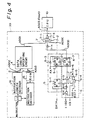
- Figure 4 shows an embodiment of a data length deciding circuit 30.
- the data length deciding circuit 30 has a conventional data length specifying circuit 4.
- This data length specifying circuit 4 is the same as that of Fig. 1, and receives an indirectly specified data length output 2 (A002) from a decoder 16, as well as a directly specified data length output 3 (A003) from a microprogram ROM 15.
- the data length specifying circuit 4 is connected to a selecting circuit 7, and provides the selecting circuit 7 with a data length specifying signal (A001) according to an instruction.
- the data length deciding circuit 30 also has a data length information storing circuit 5 of one to several bits for storing data length information.
- the storing circuit 5 comprises latches 5-1 and 5-2, and an inverter 5-3.
- An input D of the latch 5-1 receives a data length input DATA
- the inverter 5-3 receives a clock signal KA.
- the latch 5-2 stores (half-state-latches) the data length information and outputs a data length indication bit (A00C) to the selecting circuit 7.
- the data length deciding circuit 30 further has a controlling circuit 6.
- the controlling circuit 6 includes a storing element of one to several bits for selecting a method of specifying data length information.
- the controlling circuit 6 comprises a NAND gate 6-1, an inverter 6-2, a NOR gate 6-3, an OR gate 6-4, an AND gate 6-5, a NOR gate 6-6, and a latch 6-7.
- One input of the NAND gate 6-1 is connected to an input/output portion 6-8 which receives an instruction execution indication signal such as an IIOS, and the other input of NAND gate 6-1 receives a clock signal KB.
- the clock signals KB and KA are non-overlapping clock signals.
- One input of the OR gate 6-4 forms a stop portion 6-9 for receiving an instruction end indication signal such as a signal IRR, and the other input of the OR gate 6-4 receives a reset signal RST.
- the latch 6-7 stores (half-state-latches), for example, the instruction execution indication signal IIOS, and outputs a specifying method selecting signal (A00D).
- the data length information storing circuit 5 has the latch circuits 5-1 and 5-2. This arrangement is suitable when data length information for an instruction that is not included in the microprograms is represented by 1 or 0 (for example, 1 for 16-bit length and 0 for eight-bit length). When a more complicated data length is employed, a combination of a plurality of latch circuits may be employed. The reason why the invention provides the storing circuit 5 is because, when an instruction which is not included in the microprograms is repeatedly executed, it is troublesome to read data each time. To solve this, the data is stored in the storing circuit 5 and repeatedly used.
- An input portion 5-4 of the storing circuit 5 is connected to a storage unit (numeral 9 of Fig. 3) such as a table for storing data length information (data) necessary for executing other processes that cannot be handled by the original microprograms.
- a storage unit such as a table for storing data length information (data) necessary for executing other processes that cannot be handled by the original microprograms.
- the controlling circuit 6 is actuated to let the storing circuit 5 read data out of the storage unit (table) and store the data in the latch circuits 5-1 and 5-2.
- the storing circuit 5 provides the selecting circuit 7 with a data length output A00C. If the output signal of the controlling circuit 6 is of level L in Fig. 4, the selecting circuit 7 cuts the output A001 of the data length specifying circuit 4 while selecting the output of the storing circuit 5, and outputs the selected one to a central processing unit 10.
- the selecting circuit 7 cuts the output of the storing circuit 5, and again selects the output of the data length specifying circuit 4 to output the selected one to the central processing unit 10.
- the selecting circuit 7 comprises two AND gates 7-1 and 7-2, and a NOR gate 7-3.
- the first AND gate 7-1 receives the output A001 of the data length specifying circuit 4 as well as the output A00D of the controlling circuit 6.
- the output of the AND gate 7-1 is connected to one input of the NOR gate 7-3.
- the second AND gate 7-2 receives the output A00C of the storing circuit 5 and the output A00D of the controlling circuit 6 through an inverter 7-4.
- the output of the AND gate 7-2 is connected to the other input of the NOR gate 7-3.
- the output of the NOR gate 7-3 is an output D out of the selecting circuit 7.
- the instruction execution indication signal IIOS indicates the execution of a process that is not included in original instruction codes.
- clocks KA and KB are provided at the timing shown in the figure, that the directly specified output A003 and indirectly specified output A002 are provided as shown in the figure, and that only one of the outputs A002 and A003 is selected by the data length specifying circuit 4 and provided to the CPU 10.
- a flip-flop formed by the NOR gate 6-3, OR gate 6-4, AND gate 6-5, and NOR gate 6-6) of the controlling circuit 6 changes to "0" in response to the clock signal KA. Namely, the controlling circuit 6 stores "0.” As a result, the output A00D of the latch 6-7 is "0" so that the value A00C latched in the latch 5-2 of the data length information storing circuit 5 is selected by the selecting circuit 7 and provided as the output A003 to the CPU 10.
- the value of the flip-flop (6-3 to 6-6) returns to "1" because the instruction executionindication signal IIOS has returned to "0.”
- the value A00D of the latch 6-7 becomes "1.”
- the selecting circuit 7 selects the output A001 of the data length specifying circuit 4 and provides the selected one as the output A003 to the CPU 10.
- the data length information input DATA is latched in the two stages of the latches 5-1 and 5-2 in response to the clock signal KB.
- the output A00B of the latch circuit 5-1 changes at time T2' slightly after the time T2
- the output A00C of the latch circuit 5-2 changes at time T4 when the next clock pulse KB occurs.
- the selecting circuit 7 is switched, and at the time T4, the output of the storing circuit 5 is sent as the output A003 to the CPU 10.
- the end signal IRR is provided to the stop portion 6-9, and the output of the NOR gate 6-3 changes from “0" to “1” at time T6 in response to the clock pulse KB.
- the output A00D of the latch circuit 6-7 changes from “0" to "1.”
- the selecting circuit 7 is switched to send the output A001 of the data length specifying circuit 4 to the CPU 10.
- a period X between T3 and T7 is the period for executing the process IIOS, where a data length necessary for executing an instruction not included in the microprograms is specified.
- the process is a sort of interrupt process. During this period, an operation is executed according to the information of the signal A00C based on the input DATA. During a period other than the period X, a process is carried out according to the output A001 of the data length specifying circuit 4.
- the above embodiments relate to deciding a data length.
- the present invention is also applicable for deciding a transferring data length and the data length of an incrementer or of a decrementer.
- the data length specifying circuit 4 can indirectly specify a data length so that two instructions which perform the same operation but with different data lengths can be described by a single microprogram. Even for a process such as an interrupt process whose data length cannot be specified with a special instruction code, the invention can decide the data length by the use of the controlling circuit 6, which switches the normal data length specifying mode to a different data specifying mode to take data length information out of the data length information storing element 5. Unlike the conventional circuit, it is not necessary to use an ALU, etc., to check data length information stored in a storing unit and branch microprograms. The invention does not use microprograms frequently, thereby reducing the size of the microprogram ROM 15.
- the controlling circuit 6 may have a storage capacity of one bit (or several bits), so that it may be realized with less hardware.
- two or more instructions having different data lengths can be described by a single microprogram, thereby reducing the size of a microprogram ROM.
Landscapes
- Engineering & Computer Science (AREA)
- Theoretical Computer Science (AREA)
- Software Systems (AREA)
- Physics & Mathematics (AREA)
- General Engineering & Computer Science (AREA)
- General Physics & Mathematics (AREA)
- Executing Machine-Instructions (AREA)
- Document Processing Apparatus (AREA)
Description
Claims (3)
- An information processing apparatus for processing information involving a plurality of instructions having different data lengths by the use of microprograms after judging data length information related to each of the instructions according to a method of indirectly specifying the data length information or a method of directly specifying the data length information in the microprograms, comprising:a data length specifying means (4) for specifying one of the directly specified data length information and indirectly specified data length information characterised in that the apparatus further comprises:a storing means (5) for storing data length information related to a process not included in the microprograms;a controlling means (6) for controlling the storing means (5); and,a selecting means (7) for selecting the output of one of the data length specifying means (4) and storing means (5), wherein information to be stored in the storing means (5) is read out from an external information storing unit that is different from the storing means in response to an operation of the controlling means (6), and is stored in the storing means (5).
- An information processing apparatus as set forth in claim 1, wherein the selecting means (7) selects one of the outputs of the data length specifying means (4) and storing means (5) in response to an output of the controlling means (6), and outputs the selected one.
- An information processing apparatus as set forth in claim 1, wherein the controlling means (6) comprises an input/output portion (6-8) for transferring predetermined data length information from the external information storing unit to the storing means (5) and for providing selecting means (7) with the information stored in the storing means (5), and a stop portion (6-9) for stopping the provision of the information to the selecting means (8).
Applications Claiming Priority (2)
| Application Number | Priority Date | Filing Date | Title |
|---|---|---|---|
| JP71127/90 | 1990-03-20 | ||
| JP2071127A JPH03271829A (en) | 1990-03-20 | 1990-03-20 | Information processor |
Publications (3)
| Publication Number | Publication Date |
|---|---|
| EP0448317A2 EP0448317A2 (en) | 1991-09-25 |
| EP0448317A3 EP0448317A3 (en) | 1992-01-02 |
| EP0448317B1 true EP0448317B1 (en) | 1998-06-10 |
Family
ID=13451597
Family Applications (1)
| Application Number | Title | Priority Date | Filing Date |
|---|---|---|---|
| EP91302287A Expired - Lifetime EP0448317B1 (en) | 1990-03-20 | 1991-03-18 | Information processing apparatus for variable length data |
Country Status (5)
| Country | Link |
|---|---|
| US (1) | US5604876A (en) |
| EP (1) | EP0448317B1 (en) |
| JP (1) | JPH03271829A (en) |
| KR (1) | KR940002478B1 (en) |
| DE (1) | DE69129560T2 (en) |
Families Citing this family (6)
| Publication number | Priority date | Publication date | Assignee | Title |
|---|---|---|---|---|
| US5809273A (en) * | 1996-01-26 | 1998-09-15 | Advanced Micro Devices, Inc. | Instruction predecode and multiple instruction decode |
| US6425070B1 (en) * | 1998-03-18 | 2002-07-23 | Qualcomm, Inc. | Variable length instruction decoder |
| AU2003252566A1 (en) | 2002-08-19 | 2004-03-03 | Kolon Ind. Inc. | Microorganism producing hyaluronic acid and purification method of hyaluronic acid |
| JP3886870B2 (en) | 2002-09-06 | 2007-02-28 | 株式会社ルネサステクノロジ | Data processing device |
| US8935512B2 (en) * | 2006-11-21 | 2015-01-13 | Nec Corporation | Instruction operation code generation system |
| US8281109B2 (en) * | 2007-12-27 | 2012-10-02 | Intel Corporation | Compressed instruction format |
Family Cites Families (3)
| Publication number | Priority date | Publication date | Assignee | Title |
|---|---|---|---|---|
| US4586130A (en) * | 1983-10-03 | 1986-04-29 | Digital Equipment Corporation | Central processing unit for a digital computer |
| US4649477A (en) * | 1985-06-27 | 1987-03-10 | Motorola, Inc. | Operand size mechanism for control simplification |
| JPH0827716B2 (en) * | 1985-10-25 | 1996-03-21 | 株式会社日立製作所 | Data processing device and data processing method |
-
1990
- 1990-03-20 JP JP2071127A patent/JPH03271829A/en active Pending
-
1991
- 1991-03-18 EP EP91302287A patent/EP0448317B1/en not_active Expired - Lifetime
- 1991-03-18 DE DE69129560T patent/DE69129560T2/en not_active Expired - Fee Related
- 1991-03-19 US US07/671,318 patent/US5604876A/en not_active Expired - Fee Related
- 1991-03-20 KR KR1019910004401A patent/KR940002478B1/en not_active Expired - Fee Related
Also Published As
| Publication number | Publication date |
|---|---|
| DE69129560D1 (en) | 1998-07-16 |
| JPH03271829A (en) | 1991-12-03 |
| KR940002478B1 (en) | 1994-03-24 |
| KR910017295A (en) | 1991-11-05 |
| DE69129560T2 (en) | 1998-10-15 |
| EP0448317A2 (en) | 1991-09-25 |
| US5604876A (en) | 1997-02-18 |
| EP0448317A3 (en) | 1992-01-02 |
Similar Documents
| Publication | Publication Date | Title |
|---|---|---|
| EP0231928B1 (en) | Program control circuit | |
| EP0169565B1 (en) | Microprocessor compatible with any software represented by different types of instruction formats | |
| US5511173A (en) | Programmable logic array and data processing unit using the same | |
| US4774688A (en) | Data processing system for determining min/max in a single operation cycle as a result of a single instruction | |
| EP0081357A1 (en) | Branch predicting computer | |
| EP0476722B1 (en) | Data processing system | |
| US4694391A (en) | Compressed control decoder for microprocessor system | |
| US4005391A (en) | Peripheral interrupt priority resolution in a micro program data processor having plural levels of subinstruction sets | |
| US5887129A (en) | Asynchronous data processing apparatus | |
| US4791551A (en) | Microprogrammable devices using transparent latch | |
| US5696957A (en) | Integrated circuit comprising a central processing unit for executing a plurality of programs | |
| EP0448317B1 (en) | Information processing apparatus for variable length data | |
| EP0110227A2 (en) | Control memory organization | |
| KR920003180B1 (en) | Data Processing Device with Bypass Circuit | |
| US5274792A (en) | Information processing apparatus with parallel instruction decoding | |
| US5539900A (en) | Information processing system | |
| US5938758A (en) | Microprocessor having function of prefetching instruction | |
| US5479620A (en) | Control unit modifying micro instructions for one cycle execution | |
| EP0136699B1 (en) | Programmable controller | |
| EP0416345B1 (en) | Instruction decoder for a pipeline processor | |
| EP0343668B1 (en) | Normalization control system for floating point arithmetic operations | |
| US6005502A (en) | Method for reducing the number of bits needed for the representation of constant values in a data processing device | |
| JPS6236575B2 (en) | ||
| US5768554A (en) | Central processing unit | |
| JP3647078B2 (en) | Processor |
Legal Events
| Date | Code | Title | Description |
|---|---|---|---|
| PUAI | Public reference made under article 153(3) epc to a published international application that has entered the european phase |
Free format text: ORIGINAL CODE: 0009012 |
|
| AK | Designated contracting states |
Kind code of ref document: A2 Designated state(s): DE FR GB |
|
| PUAL | Search report despatched |
Free format text: ORIGINAL CODE: 0009013 |
|
| AK | Designated contracting states |
Kind code of ref document: A3 Designated state(s): DE FR GB |
|
| 17P | Request for examination filed |
Effective date: 19920619 |
|
| 17Q | First examination report despatched |
Effective date: 19961007 |
|
| GRAG | Despatch of communication of intention to grant |
Free format text: ORIGINAL CODE: EPIDOS AGRA |
|
| GRAG | Despatch of communication of intention to grant |
Free format text: ORIGINAL CODE: EPIDOS AGRA |
|
| GRAH | Despatch of communication of intention to grant a patent |
Free format text: ORIGINAL CODE: EPIDOS IGRA |
|
| GRAH | Despatch of communication of intention to grant a patent |
Free format text: ORIGINAL CODE: EPIDOS IGRA |
|
| GRAA | (expected) grant |
Free format text: ORIGINAL CODE: 0009210 |
|
| AK | Designated contracting states |
Kind code of ref document: B1 Designated state(s): DE FR GB |
|
| REF | Corresponds to: |
Ref document number: 69129560 Country of ref document: DE Date of ref document: 19980716 |
|
| ET | Fr: translation filed | ||
| PLBE | No opposition filed within time limit |
Free format text: ORIGINAL CODE: 0009261 |
|
| STAA | Information on the status of an ep patent application or granted ep patent |
Free format text: STATUS: NO OPPOSITION FILED WITHIN TIME LIMIT |
|
| 26N | No opposition filed | ||
| REG | Reference to a national code |
Ref country code: GB Ref legal event code: IF02 |
|
| PGFP | Annual fee paid to national office [announced via postgrant information from national office to epo] |
Ref country code: FR Payment date: 20020312 Year of fee payment: 12 |
|
| PGFP | Annual fee paid to national office [announced via postgrant information from national office to epo] |
Ref country code: GB Payment date: 20020320 Year of fee payment: 12 |
|
| PGFP | Annual fee paid to national office [announced via postgrant information from national office to epo] |
Ref country code: DE Payment date: 20020327 Year of fee payment: 12 |
|
| PG25 | Lapsed in a contracting state [announced via postgrant information from national office to epo] |
Ref country code: GB Free format text: LAPSE BECAUSE OF NON-PAYMENT OF DUE FEES Effective date: 20030318 |
|
| PG25 | Lapsed in a contracting state [announced via postgrant information from national office to epo] |
Ref country code: DE Free format text: LAPSE BECAUSE OF NON-PAYMENT OF DUE FEES Effective date: 20031001 |
|
| GBPC | Gb: european patent ceased through non-payment of renewal fee |
Effective date: 20030318 |
|
| PG25 | Lapsed in a contracting state [announced via postgrant information from national office to epo] |
Ref country code: FR Free format text: LAPSE BECAUSE OF NON-PAYMENT OF DUE FEES Effective date: 20031127 |
|
| REG | Reference to a national code |
Ref country code: FR Ref legal event code: ST |