EP0446954A2 - Control system for excitation of synchronous machine - Google Patents
Control system for excitation of synchronous machine Download PDFInfo
- Publication number
- EP0446954A2 EP0446954A2 EP91104073A EP91104073A EP0446954A2 EP 0446954 A2 EP0446954 A2 EP 0446954A2 EP 91104073 A EP91104073 A EP 91104073A EP 91104073 A EP91104073 A EP 91104073A EP 0446954 A2 EP0446954 A2 EP 0446954A2
- Authority
- EP
- European Patent Office
- Prior art keywords
- phase
- signals
- output
- portions
- failure
- Prior art date
- Legal status (The legal status is an assumption and is not a legal conclusion. Google has not performed a legal analysis and makes no representation as to the accuracy of the status listed.)
- Granted
Links
- 230000001360 synchronised effect Effects 0.000 title claims abstract description 23
- 230000005284 excitation Effects 0.000 title claims abstract description 21
- 238000004804 winding Methods 0.000 claims abstract description 3
- 238000001514 detection method Methods 0.000 claims description 18
- 238000010304 firing Methods 0.000 description 8
- 238000010586 diagram Methods 0.000 description 4
- 230000005856 abnormality Effects 0.000 description 1
Images

Classifications
-
- G—PHYSICS
- G05—CONTROLLING; REGULATING
- G05B—CONTROL OR REGULATING SYSTEMS IN GENERAL; FUNCTIONAL ELEMENTS OF SUCH SYSTEMS; MONITORING OR TESTING ARRANGEMENTS FOR SUCH SYSTEMS OR ELEMENTS
- G05B9/00—Safety arrangements
- G05B9/02—Safety arrangements electric
- G05B9/03—Safety arrangements electric with multiple-channel loop, i.e. redundant control systems
-
- H—ELECTRICITY
- H02—GENERATION; CONVERSION OR DISTRIBUTION OF ELECTRIC POWER
- H02H—EMERGENCY PROTECTIVE CIRCUIT ARRANGEMENTS
- H02H7/00—Emergency protective circuit arrangements specially adapted for specific types of electric machines or apparatus or for sectionalised protection of cable or line systems, and effecting automatic switching in the event of an undesired change from normal working conditions
- H02H7/06—Emergency protective circuit arrangements specially adapted for specific types of electric machines or apparatus or for sectionalised protection of cable or line systems, and effecting automatic switching in the event of an undesired change from normal working conditions for dynamo-electric generators; for synchronous capacitors
- H02H7/065—Emergency protective circuit arrangements specially adapted for specific types of electric machines or apparatus or for sectionalised protection of cable or line systems, and effecting automatic switching in the event of an undesired change from normal working conditions for dynamo-electric generators; for synchronous capacitors against excitation faults
-
- H—ELECTRICITY
- H02—GENERATION; CONVERSION OR DISTRIBUTION OF ELECTRIC POWER
- H02P—CONTROL OR REGULATION OF ELECTRIC MOTORS, ELECTRIC GENERATORS OR DYNAMO-ELECTRIC CONVERTERS; CONTROLLING TRANSFORMERS, REACTORS OR CHOKE COILS
- H02P9/00—Arrangements for controlling electric generators for the purpose of obtaining a desired output
- H02P9/10—Control effected upon generator excitation circuit to reduce harmful effects of overloads or transients, e.g. sudden application of load, sudden removal of load, sudden change of load
Abstract
Description
- The present invention relates to an excitation control system provided to a synchronous machine such as a synchronous generator or a synchronous electric motor or the like, and more particularly, to an excitation control system for synchronous machines that are duplicated so as to increase the reliability.
- In general, excitation control systems for synchronous machines have a basic function to perform automatic voltage regulation functions so as to control a terminal voltage of the synchronous machines to be constant, with ancillary functions being an overexcitation limit function and an underexcitation limit function so that the operation of the synchronous machine is stable and within the critical limits. Furthermore, there is also a control system provided with many complex functions such as secondary regulation functions so that the performance and the ineffective power are stable.
- However, when there is the generation of a failure in such an excitation control system, a control abnormality generates and the control operation stops so that it is no longer possible to continue the operation of the synchronous machine. Accordingly, it is required that there be a high reliability of excitation control systems. In particular, in cases when there is a large-capacity synchronous generator provided to operating power facilities, it is necessary that there always be an extremely high reliability from the point of view of the public nature and the social importance of power supply.
- Control systems for which such extremely high reliability is demanded are generally such that there is duplicated configuration of control systems so that the reliability of the control system itself is increased so as to prevent the generation of failures and so that it is possible to continue the operation of the machines that are the object of control even if a failure should generate.
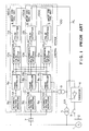
- FIG. 1 is a view showing the configuration of a conventional example of an excitation control system for synchronous machines that have a duplicated configuration.
- In the figure, a field winding 2 of a
synchronous machine 1 is supplied via afield circuit breaker 3, with an excitation current from athyristor rectifier apparatus 4 that has three-phase uniform bridge wiring, and the AC power EA from thisthyristor rectifier apparatus 4 is supplied via anexcitation transformer 5 from the output of thesynchronous machine 1. - As shown in FIG. 1, a
control system 100 comprises an A group control unit 100A, a Bgroup control unit 100B and a C group control unit 100C, for respectively controlling an excitation of A-C groups. -
Automatic voltage regulators synchronous machine 1 via the potential transformer 7 and perform control calculations so that this terminal voltage becomes equal to the objective value (set value), and outputs the control signals CA, CB and CC. -
Phase controllers transformer 9 and this AC power voltage is output as the reference phase as the phase signals PA, PB and PC that change in accordance with the control signals CA, CB and CC. -
Intermediate pulse selectors - Pulse outputters 11a, 11b and 11c output arc pulses in the phase indicated by the phase signals PLA, PLB and PLC and the configuration is such that this output is connected by logical sum, and so that the firing pulses PL are supplied to the
thyristor rectifier apparatus 4. - When there is normal operation, the
automatic voltage regulators phase controllers automatic voltage regulators phase controllers - The
intermediate pulse selectors - Accordingly, the firing pulses that are output by the pulse outputters 11a, 11b and 11c become the same signals and the firing pulse PL which is the logical sum of them is also the same signal.
- FIG. 2 is a view showing the configuration of the
intermediate pulse selector 10a and is a majority circuit comprising an AND circuit (logical product) 12A, 12B and 12C and an OR circuit (logical sum) 13a and so the phase signals PLA become the majority result of the phase signals PA, PB and PC. Moreover, the otherintermediate pulse selectors 10b and 10c have the same configuration as theintermediate pulse selector 10a. - FIG. 3 is a view showing the waveform indicating the operation of a conventional excitation control system. The
thyristor rectifier apparatus 4 has a three-phase uniform bridge wiring and so the firing pulses PL and the phase PA, PB, PC, PLA, PLB and PLC are each signals of the six phases but in FIG. 3, only one phase portion of there is indicated. In addition, the phase signals PLA, PLB and PLC become the same signal and so only the phase signal PLA is shown. - A cycle t₁ of the AC power EA shows the normal operation and the phase signals PA, PB and PC shown in FIG. 3(a) each become signals that are proportional to the control signals CA, CB and CC with each of the phases of the AC power EA being the reference, as shown in FIG. 3(b) through (d). As shown in FIG. 3(e), the phase signals PLA become the majority result of the phase signals PA, PB and PC and so for the cycle t₁, become the same signal as the phase signals PA. More specifically, the phase signal PLA selects the phase signal PA that indicates the intermediate phase of the three phase signals PA, PB and PC. The firing pulse PL becomes the pulse signal of a predetermined width from the rise of the phase signal PLA.
- Then, the cycle t₂ shows the operation when either or both of the automatic
voltage adjuster portion 6a or thephase control portion 8a fails and the phase signal PA is no longer output. In this case, the phase signal PLA is the result of the logical product of the phase signals PB and PC and so becomes the same signal as the phase signal PC. - Furthermore, the cycle t₃ shows the operation for the status where the phase signal PA is no longer output and either or both of the
automatic voltage regulator 6b and thephase control portion 8b has failed and the phase signal PB is no longer output. In this case, the phase signal PLA is no longer output and so the firing pulse PL is also not output. - In such a conventional excitation control apparatus, even if there is a failure on one system of the
automatic voltage regulators phase control portions pulse selector portions - The present invention has as an object the provision of an excitation control system that has an extremely high reliability and that can continue normal operation even if two of the triplicated control systems fail.
- In order to attain this objective, in the present invention, the intermediate pulse selector portions select the phase signals of the intermediate phase from the phase signals that are output from the triplicated phase control portions and automatic voltage regulator portions, and when any one of the triplicated phase control portions and automatic voltage regulator portions fails, either of the phase signals output from the other two systems is selected so as to select the phase signals output from the other system.
- By this, normal phase signals are always selected even if one or two of the systems of the triplicated phase control portions and automatic voltage regulator portions fails.
- As has been described above, according to the present invention, it is possible to select and output normal phase signals even if one or two of the systems of the triplicated phase control portions and automatic voltage regulator portions fails and to use this output as the basis for the supply of firing pulses to a thyristor rectifier apparatus and therefore enable provide an excitation control system for synchronous machines and that has an extremely high reliability and that enables the continuous operation of the synchronous machines.
- In the appended drawings,
- FIG. 1 is a view showing the configuration of a conventional excitation control system;
- FIG. 2 is a view showing the configuration of a conventional intermediate pulse selector portion;
- FIG. 3 is a waveform diagram showing the operation of a conventional excitation control system;
- FIG. 4 is a view showing the configuration of a first embodiment of the excitation control system according to the present invention;
- FIG. 5 is a view showing the configuration of an intermediate pulse selector portion of a first embodiment of the excitation control system according to the present invention;
- FIG. 6 is a view describing the truth value table of the intermediate pulse selector portion described above; and
- FIG. 7 is waveform diagram showing the operation of a control system relating to an embodiment of the present invention.
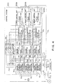
- FIG. 4 is a view showing the configuration of a first embodiment of the excitation control system according to the present invention. In the figure, those portions that correspond to portions of FIG. 1 are indicated with corresponding numerals and the corresponding descriptions of them are omitted.
- A
control system 200 shown in FIG. 4 comprises an Agroup control unit 200A, a Bgroup control unit 200B, a Cgroup control unit 200C, and afailure detection unit 20 which detects each failure of A-C groups. -
Intermediate pulse selectors - The failure signal DA is turned on (hereinafter referred to as the "H" signal level) when there is a failure in either of the
automatic voltage regulator 6a or thephase controller 8a of the A group, as detected by the OR circuit 20a of thefailure detection unit 20. In the same manner as for the failure signal DA, the failure signals DB and DC become "H" when there is a failure in either or both of theautomatic voltage regulators phase controllers OR circuits - As shown in FIG. 4, in each A
group control unit 200A, Bgroup control unit 200B and Cgroup control unit 200C, theautomatic voltage regulator failure detector regulator phase controller failure detector 31a, 31b or 31c for outputting a detection signal GA, GB or GC, respectively, when it detects a failure of thecontroller - The
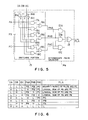
failure detection unit 20 comprises the OR circuit 20a for outputting the failure signal DA which is a logical sum of the detection signals FA and GA respectively output from thefailure detectors OR circuit 20b for outputting the failure signal DB which is a logical sum of the detection signals FB and GB respectively output from thefailure detectors 30b and 31b, and theOR circuit 20c for outputting the failure signal DC which is a logical sum of the detection signals FC and GC respectively output from thefailure detectors 30c and 31c. All these failure signals DA, DB and DC are supplied to all of theintermediate pulse selectors - FIG. 5 is a view showing the configuration of an intermediate
pulse selector portion 14a, and in the figure, those portions that correspond to portions of FIG. 2 are indicated with corresponding numerals and the corresponding descriptions of them are omitted. Aswitching portion 15 outputs the phase signals PHA, PHB and PHC corresponding to the phase signals PA, PB and PC, and when the failure signals DA, DB and DC are all "L", the phase signals PHA, PHB and PHC are all the same value as the phase signals PA, PB and PC. - More specifically, this
switching portion 15 is configured frominverters circuits circuits OR circuits aforementioned AND circuits - When two of the failure signals DA, DB and DC are at the "H" level, one of the corresponding phase signals PHA, PHB and PHC becomes the "H" level and the other becomes the "L" level.
- When all of the failure signals DA, DB and DC are at the "H" level, the phase signals PHA, PHB and PHC all become the "L" level.
- The phase signals PLA shows the majority result of the phase signals PHA, PHB and PHC.
- FIG. 6 is a view describing the truth value table of the intermediate
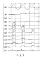
pulse selector portion 14a with respect to the failure signals DA, DB and DC. As can be seen from the diagram, the phase signals PLA become the majority result of the phase signals PA, PB and PC when all of the failure signals DA, DB and DC are the "L" level. In addition, when either of the failure signals DA, DB and DC is at the "H" level, the logical sum of the two that of the phase signals PA, PB and PC that do not correspond to a failures is taken. Furthermore, when two of the failure signals DA, DB and DC are at the "H" level, the one of the phase signals PA, PB and PC that does not correspond to a failure becomes the phase signal PLA. - FIG. 7 is a waveform diagram showing the operation of the
control system 200 relating to the embodiment of the present invention. - The cycle t₁ of the AC power shown in FIG. 7(a) shows normal operation, and the phase signals PA, PB and PC become signals that are proportional to the control signals CA, CB and CC, with the phases of the each of the AC power EA being the reference.
- In FIG. 7(b) through (d), each of the failure signals DA, DB and DC show the "L" level and so the phase signals PHA, PHB and PHC becomes the same as each of the phase signals PA, PB and PC as shown in FIG. 7(e) through (g). Accordingly, the phase signals PLA become the same signals as the phase signals PA at the cycle t₁. The arc pulse PL becomes the pulse signal with a predetermined width from the rise of the phase signal PLA.
- Then, the cycle t₂ shows the operation for the case when either or both of the
automatic voltage regulator 6a and thephase controller 8a fails, and the phase signal PA is not output. - In this case, the failure signal DA becomes the "H" level as shown in FIG. 7(b) and so the phase signal PHA becomes "H" irrespective of the status of the phase signal PA and as shown in FIG. 7(h), and the phase signal PLA becomes the result of the logical sum of the phase signals PB and PC, as shown in FIG. 7(k). Accordingly, at the cycle t₂, the phase signals PLA become the same signal as the phase signal PB.
- Furthermore, cycle t₃ shows the operation for the status where the phase signal PA is not output, and either or both of the
automatic voltage regulator 6b andphase controller 8b fails, and the phase signal PB is no longer output. - In this case, as shown in FIG. 7(b) and (c), the failure signals DA and DB become the "H" level and so the phase signals PHA become the "H" level irrespective of the status of the phase signal PA, as shown in FIG. 7(h), and the phase signals PHB of FIG. 7(i) become the "L" level irrespective of the status of the phase signal PB, and at the cycle t₃, the phase signal PLA of FIG. 7(k) becomes the same signal as the phase signal PC of FIG. 7(g).
- As has been described above, even if one or two systems of the triplicated
automatic voltage regulators triplicated phase controllers intermediate pulse selectors synchronous machine 1 can continue to operate normally.
Claims (6)
- An excitation control apparatus for a synchronous machine and configured from automatic voltage regulator portions (6a, 6b, 6c) that output control signals (CA, CB, CC) so as to regulate a terminal voltage of a synchronous machine (1), phase control portions (8a, 8b, 8c) that output phase signals (PA, PB, PC) so as to control the phase of an arc pulse (PL) of a thyristor rectifier apparatus that supplies a field current to a field winding (2) of said synchronous machine (1), intermediate pulse selector portions [14(10)] provided with three pulse output portions (11a, 11b, 11c) that output said arc pulse (PL) on the basis of said phase signals (PA, PB, PC) and which are provided between aforementioned three pulse output portions (11a, 11b, 11c) and phase control portions (8a, 8b, 8c) provided between pulse output portions (11a, 11b, 11c) and said three phase control portions (8a, 8b, 8c), a logical sum of said three arc pulses being supplied to said thyristor rectifier apparatus;
characterized in that said intermediate pulse selector portions (14) select a phase signal of an intermediate phase from said three phase signals (PA, PB, PC), phase signals from one of another two groups being selected and output when one pair of said three automatic voltage regulator portions (6a, 6b, 6c) and phase control portions (8a, 8b, 8c) fails, and phase signals output from the unfailed pair being selected and output when two of said three automatic voltage regulator portions (6a, 6b, 6c) and phase control portions (8a, 8b, 8c) fails. - The control system of claim 1, wherein:
each of said intermediate pulse selector portion (14a, 14b, 14c) receives the supply of failure signals (DA, DB, DC) output from a failure detector circuit (20) that detects whether or not a pair (6a and 8a, 6b and 8b, 6c and 8c) of said three pairs of automatic voltage regulator (6a, 6b, 6c) and phase control portions (8a, 8b, 8c) has failed on the basis of detection signals (FA, FB, FC and GA, GB, GC) respectively output from respective failure detectors (30a-30c and 31a-31c). - The control system of claim 2, wherein:
said failure detection circuit (20) comprises a first OR circuit (20a) that takes a logical sum of said detection signal (GA) from said detector (31a) of said first phase control portion (8a) and said detection signal (FA) from said detector (30a) of a first automatic voltage regulator portion (6a) and outputs the first failure signal (DA) to first through third intermediate pulse selector portions (14a, 14b, 14c), a second OR circuit (20b) that takes a logical sum of said detection signal (GB) from said detector (31b) of said second phase control portion (8b) and said detection signal (FA) from said detector (30b) of said second automatic voltage regulator (6b) and outputs the second failure signal (DB) to first through third intermediate pulse selector portions (14a, 14b, 14c), and a third OR circuit (20c) that takes a logical sum of said detection signal (GC) from said detector (31c) of said third phase control portion (8c) and said detection signal (FC) from said detector (30c) of said third automatic voltage regulator (6a) and outputs the third failure signals (DA) to first through third intermediate pulse selector portions (14a, 14b, 14c). - The control system of claim 1, wherein:
one intermediate pulse selector of said intermediate pulse selector portions (14a, 14b, 14c) of A to C groups comprises a switching portion (15) that outputs phase signals (PHA, PHB, PHC) on the basis of said failure signals (DA, DB, DC) that indicate failure of any of said pairs (6a and 8a, 6b and 8b, 6c and 8c) and said phase signals (PA, PB, PC), and a plural number of logical elements (12A, 12B, 12C) that by the logical calculation of said phase signals (PHA, PHB, PHC), output phase signals (PLA, PLB, PLC) that are majority result of said signals (PHA, PHB, PHC). - The control system of claim 4, wherein:
said switching portion (15) comprises first, second and third inverters (16A, 16B, 16C) that invert said first, second and third failure signals (DA, DB, DC), first through third AND circuits (17A, 17B, 17C) that take the logical product of said signals output from said first, second and third inverters with respect to said first, second and third phase signals (PA, PB, PC), fourth through sixth AND circuits (18A, 18B, 18C) that take the logical product between a signal output from said third inverter (16C) and said first failure signal (DA), between a signal output from said first inverter (16A) and said second failure signal (B), and between a signal output from said second inverter (16B) and said third failure signal (DC), respectively, and first through third OR circuits (19A, 19B, 19C) that respectively take the logical sum of outputs of first and fourth AND circuits (17A, 17B), second and fifth AND circuits (17B, 18B) and third and sixth AND circuits (17C, 18C) and respectively output said phase signals (PHA, PHB, PHC). - The control system of claim 4, wherein:
said logical elements (12A, 12B, 12C and 13) comprise first through third AND circuits (12A, 12B, 12C) that respectively take the logical sum of first and second signals (PHA, PHB), second and third signals (PHB, PHC), and third and first signals (PHC, PHA) of said phase signals, and an OR circuit (13) that inputs all of the outputs of said first through third AND circuits (12A, 12B, 12C), takes the logical sum, and outputs said phase signals (PLA, PLB, PLC) that indicate a majority result of said phase signals (PHA, PHB, PHC).
Applications Claiming Priority (2)
| Application Number | Priority Date | Filing Date | Title |
|---|---|---|---|
| JP64123/90 | 1990-03-16 | ||
| JP2064123A JP3017765B2 (en) | 1990-03-16 | 1990-03-16 | Excitation controller for synchronous machine |
Publications (3)
| Publication Number | Publication Date |
|---|---|
| EP0446954A2 true EP0446954A2 (en) | 1991-09-18 |
| EP0446954A3 EP0446954A3 (en) | 1992-08-05 |
| EP0446954B1 EP0446954B1 (en) | 1996-10-09 |
Family
ID=13248980
Family Applications (1)
| Application Number | Title | Priority Date | Filing Date |
|---|---|---|---|
| EP91104073A Expired - Lifetime EP0446954B1 (en) | 1990-03-16 | 1991-03-15 | Control system for excitation of synchronous machine |
Country Status (5)
| Country | Link |
|---|---|
| US (1) | US5200691A (en) |
| EP (1) | EP0446954B1 (en) |
| JP (1) | JP3017765B2 (en) |
| CA (1) | CA2038424C (en) |
| DE (1) | DE69122533T2 (en) |
Cited By (2)
| Publication number | Priority date | Publication date | Assignee | Title |
|---|---|---|---|---|
| EP0556481A1 (en) * | 1992-02-17 | 1993-08-25 | Asea Brown Boveri Ag | Procedure and device for operating a synchronous machine |
| RU204929U1 (en) * | 2020-12-09 | 2021-06-17 | Открытое акционерное общество "Электроагрегат" | Synchronous brushless generator with self-excitation, built into the chassis of the vehicle |
Families Citing this family (3)
| Publication number | Priority date | Publication date | Assignee | Title |
|---|---|---|---|---|
| US20050243491A1 (en) * | 2004-04-28 | 2005-11-03 | James Tanis | Multi-function power monitor and circuit protector |
| CN101795108B (en) * | 2010-03-16 | 2012-05-02 | 东方电气集团东方电机有限公司 | Excitation control system for giant machine set |
| DE102010042328A1 (en) * | 2010-10-12 | 2012-04-12 | Robert Bosch Gmbh | Method for monitoring the charging operation of an energy storage device in a vehicle and charging system for charging an energy storage device in a vehicle |
Citations (2)
| Publication number | Priority date | Publication date | Assignee | Title |
|---|---|---|---|---|
| US4472806A (en) * | 1982-05-03 | 1984-09-18 | The Boeing Company | Signal selection and fault detection apparatus |
| JPH01315300A (en) * | 1988-06-15 | 1989-12-20 | Toshiba Corp | Excitation controller |
Family Cites Families (5)
| Publication number | Priority date | Publication date | Assignee | Title |
|---|---|---|---|---|
| US3634750A (en) * | 1970-04-23 | 1972-01-11 | Westinghouse Electric Corp | Regulator apparatus responsive to generator output power factor and voltage |
| JPS4979158A (en) * | 1972-12-01 | 1974-07-31 | ||
| US4264856A (en) * | 1979-03-23 | 1981-04-28 | Basler Electric Company | System for maintaining excitation of an alternating current generator during excessive output current conditions |
| JPH0710149B2 (en) * | 1984-02-20 | 1995-02-01 | 日本電装株式会社 | Vehicle charge control device |
| JP2716778B2 (en) * | 1989-02-16 | 1998-02-18 | 株式会社東芝 | Thyristor device control circuit |
-
1990
- 1990-03-16 JP JP2064123A patent/JP3017765B2/en not_active Expired - Fee Related
-
1991
- 1991-03-15 EP EP91104073A patent/EP0446954B1/en not_active Expired - Lifetime
- 1991-03-15 DE DE69122533T patent/DE69122533T2/en not_active Expired - Fee Related
- 1991-03-15 CA CA002038424A patent/CA2038424C/en not_active Expired - Lifetime
- 1991-03-18 US US07/670,869 patent/US5200691A/en not_active Expired - Lifetime
Patent Citations (2)
| Publication number | Priority date | Publication date | Assignee | Title |
|---|---|---|---|---|
| US4472806A (en) * | 1982-05-03 | 1984-09-18 | The Boeing Company | Signal selection and fault detection apparatus |
| JPH01315300A (en) * | 1988-06-15 | 1989-12-20 | Toshiba Corp | Excitation controller |
Non-Patent Citations (1)
| Title |
|---|
| PATENT ABSTRACTS OF JAPAN vol. 14, no. 120 (E-899)6 March 1990 & JP-A-1 315 300 ( TOSHIBA ) 20 December 1989 * |
Cited By (2)
| Publication number | Priority date | Publication date | Assignee | Title |
|---|---|---|---|---|
| EP0556481A1 (en) * | 1992-02-17 | 1993-08-25 | Asea Brown Boveri Ag | Procedure and device for operating a synchronous machine |
| RU204929U1 (en) * | 2020-12-09 | 2021-06-17 | Открытое акционерное общество "Электроагрегат" | Synchronous brushless generator with self-excitation, built into the chassis of the vehicle |
Also Published As
| Publication number | Publication date |
|---|---|
| US5200691A (en) | 1993-04-06 |
| DE69122533D1 (en) | 1996-11-14 |
| JPH03270699A (en) | 1991-12-02 |
| JP3017765B2 (en) | 2000-03-13 |
| CA2038424A1 (en) | 1991-09-17 |
| EP0446954A3 (en) | 1992-08-05 |
| EP0446954B1 (en) | 1996-10-09 |
| CA2038424C (en) | 1994-07-12 |
| DE69122533T2 (en) | 1997-03-27 |
Similar Documents
| Publication | Publication Date | Title |
|---|---|---|
| EP0161283B1 (en) | Inverter control system for providing an easily filtered output | |
| KR940006837A (en) | Electric vehicle controller | |
| JPH0295143A (en) | Asynchronous multiphase switching circuit | |
| KR20020079987A (en) | PWM Cycloconverter and Power Supply Abnormality Detection | |
| US5210443A (en) | Process and apparatus for parallel control of tapped transformers | |
| EP3633465A1 (en) | Diagnostic apparatus | |
| EP0446954B1 (en) | Control system for excitation of synchronous machine | |
| GB2585855A (en) | Fault-tolerant electrical drive | |
| JP4726624B2 (en) | Inverter system | |
| RU2757695C2 (en) | Control of the number of active power elements of the speed controller | |
| EP4044417A1 (en) | Power conversion device | |
| JP3129780B2 (en) | Excitation controller for synchronous machine | |
| CN114600337A (en) | Uninterruptible power supply device | |
| KR101936564B1 (en) | Apparatus for controlling multilevel inverter | |
| JPH04365770A (en) | Control device for elevator | |
| US20230208185A1 (en) | Uninterruptible power supply apparatus | |
| JP7320331B2 (en) | Control device | |
| WO2023089683A1 (en) | Module type uninterruptible power supply device and uninterruptible power supply system | |
| JPH06233599A (en) | Excitation controller | |
| JPH07336897A (en) | Inverter device for distributed power supply and control method thereof | |
| JPH0398497A (en) | Generator exciter, synchronizer controller, and malfunction detection method for them | |
| JPH06105556A (en) | Power converter | |
| JPS63242126A (en) | Failure detector of generator | |
| JPH06209582A (en) | Parallel operation device of inverter | |
| JPS59127579A (en) | Parallel redundancy type power source |
Legal Events
| Date | Code | Title | Description |
|---|---|---|---|
| PUAI | Public reference made under article 153(3) epc to a published international application that has entered the european phase |
Free format text: ORIGINAL CODE: 0009012 |
|
| 17P | Request for examination filed |
Effective date: 19910326 |
|
| AK | Designated contracting states |
Kind code of ref document: A2 Designated state(s): CH DE LI |
|
| PUAL | Search report despatched |
Free format text: ORIGINAL CODE: 0009013 |
|
| AK | Designated contracting states |
Kind code of ref document: A3 Designated state(s): CH DE LI |
|
| 17Q | First examination report despatched |
Effective date: 19940119 |
|
| GRAG | Despatch of communication of intention to grant |
Free format text: ORIGINAL CODE: EPIDOS AGRA |
|
| GRAH | Despatch of communication of intention to grant a patent |
Free format text: ORIGINAL CODE: EPIDOS IGRA |
|
| GRAH | Despatch of communication of intention to grant a patent |
Free format text: ORIGINAL CODE: EPIDOS IGRA |
|
| GRAA | (expected) grant |
Free format text: ORIGINAL CODE: 0009210 |
|
| AK | Designated contracting states |
Kind code of ref document: B1 Designated state(s): CH DE LI |
|
| RAP1 | Party data changed (applicant data changed or rights of an application transferred) |
Owner name: KABUSHIKI KAISHA TOSHIBA |
|
| REF | Corresponds to: |
Ref document number: 69122533 Country of ref document: DE Date of ref document: 19961114 |
|
| REG | Reference to a national code |
Ref country code: CH Ref legal event code: NV Representative=s name: PATENTANWALTSBUERO FELDMANN AG |
|
| PLBE | No opposition filed within time limit |
Free format text: ORIGINAL CODE: 0009261 |
|
| STAA | Information on the status of an ep patent application or granted ep patent |
Free format text: STATUS: NO OPPOSITION FILED WITHIN TIME LIMIT |
|
| 26N | No opposition filed | ||
| REG | Reference to a national code |
Ref country code: CH Ref legal event code: PFA Owner name: KABUSHIKI KAISHA TOSHIBA Free format text: KABUSHIKI KAISHA TOSHIBA#72 HORIKAWA-CHO, SAIWAI-KU, KAWASAKI-SHI,#KANAGAWA-KEN (JP) -TRANSFER TO- KABUSHIKI KAISHA TOSHIBA#72 HORIKAWA-CHO, SAIWAI-KU, KAWASAKI-SHI,#KANAGAWA-KEN (JP) |
|
| PGFP | Annual fee paid to national office [announced via postgrant information from national office to epo] |
Ref country code: CH Payment date: 20090317 Year of fee payment: 19 |
|
| PGFP | Annual fee paid to national office [announced via postgrant information from national office to epo] |
Ref country code: DE Payment date: 20090313 Year of fee payment: 19 |
|
| REG | Reference to a national code |
Ref country code: CH Ref legal event code: PL |
|
| PG25 | Lapsed in a contracting state [announced via postgrant information from national office to epo] |
Ref country code: LI Free format text: LAPSE BECAUSE OF NON-PAYMENT OF DUE FEES Effective date: 20100331 Ref country code: CH Free format text: LAPSE BECAUSE OF NON-PAYMENT OF DUE FEES Effective date: 20100331 Ref country code: DE Free format text: LAPSE BECAUSE OF NON-PAYMENT OF DUE FEES Effective date: 20101001 |