EP0446878B1 - Image display element - Google Patents
Image display element Download PDFInfo
- Publication number
- EP0446878B1 EP0446878B1 EP19910103789 EP91103789A EP0446878B1 EP 0446878 B1 EP0446878 B1 EP 0446878B1 EP 19910103789 EP19910103789 EP 19910103789 EP 91103789 A EP91103789 A EP 91103789A EP 0446878 B1 EP0446878 B1 EP 0446878B1
- Authority
- EP
- European Patent Office
- Prior art keywords
- layer
- image display
- electron beams
- aluminum
- thickness
- Prior art date
- Legal status (The legal status is an assumption and is not a legal conclusion. Google has not performed a legal analysis and makes no representation as to the accuracy of the status listed.)
- Expired - Lifetime
Links
Images


Classifications
-
- H—ELECTRICITY
- H01—ELECTRIC ELEMENTS
- H01J—ELECTRIC DISCHARGE TUBES OR DISCHARGE LAMPS
- H01J29/00—Details of cathode-ray tubes or of electron-beam tubes of the types covered by group H01J31/00
- H01J29/02—Electrodes; Screens; Mounting, supporting, spacing or insulating thereof
- H01J29/10—Screens on or from which an image or pattern is formed, picked up, converted or stored
- H01J29/18—Luminescent screens
- H01J29/28—Luminescent screens with protective, conductive or reflective layers
Definitions
- the invention relates to a flat image display comprising a vacuum envelope having a face plate, a back cell and a plurality of vacuum cells having a potential gradient, a plurality of cathodes disposed within said vacuum envelope for radiating electron beams toward said face plate, control electrodes for controlling the electron beams radiated from said cathodes, a phosphor layer on said face plate and positioned to be irradiated by the electron beams and for emitting light when irradiated by the electron beams, and an aluminum back layer on the face of said phosphor layer towards said cathode for directing light emitted by said phosphor layer to the face of said face plate.
- a flat image display having the same light emitting principle as that of the Braun tube is known from USA patents Nos. 4,451,846 and 4,449,148.
- Such a flat image display uses electron beams from a plurality of linear thermal cathodes, controlled by a plurality of control electrodes, and colliding against a fluorescent screen. It can display letters, images and so on.
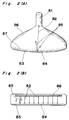
- a back electrode 51 is adapted to direct into the front face direction electron beams 72 emitted from a plurality of linear thermal cathodes 52a through 52d.
- An electron beam fetching electrode 53 fetches the electrons of the linear thermal cathode 52a through 52d.
- Through holes 62 are provided in the electrode 53 to let the electron beams 72 pass through them.
- a signal electrode 54 which is provided to apply video signals and is composed of a plurality of control electrodes 64.
- the control electrodes 64 have through holes 63 therein to let the electron beams 72 pass through it.
- a first focusing electrode 55 and a second focusing electrode 56 are provided to focus the electron beams 72 in the horizontal and vertical directions.
- a horizontal deflection electrode 68 deflects the electron beams in the right, left directions of the picture face, and is composed of one set of comb type electrodes 57a and 57b.
- the electrodes of the comb type electrodes 57a and 57b constitute a slot 67 to let the electron beams 72 pass through.
- a vertical deflection electrode 71 is provided to deflect the electron beams 72 in the vertical direction of the picture face, and is composed of a set of comb type electrodes 58a and 58b.
- the comb type electrodes 58a and 58b constitute a slot 70 between the electrodes to let the electrode beams 72 pass through it.
- a face plate (surface glass cell) 60 has a screen 73 composed of a three color phosphor layers of red, green, blue, a black stripe layer provided between them, and a metal back layer provided behind them on the inner face thereof.
- a metallic plate 61 made of a back cell, and the face plate 60 constitute a vacuum cell.
- the rearward dispersed electrons generated by the electrons applied upon the metal back layer of the face plate 60 as the interior of the display element have a potential gradient, instead of equipotential like in conventional Braun tubes, and are applied again upon the face plate, thus resulting in lowering the contrast ratio.
- Fig. 2 A, B are views showing the internal construction of a conventional Braun tube and of a conventional flat image display.
- GB-A-2 120 840 discloses a cathode ray tube of the BRAUN type in which the electron beams are accelerated through a large potential difference immediately before impact with a fluorescent screen. This acceleration is provided in a large area channel plate electron multiplier which is disposed close to the face plate of the cathode ray tube. However, within the electron multiplier there occurs impact of electrons so that dispersed secondary electron beams are caused. Accordingly, no high accuracy in deflection can be obtained as is necessary in a flat thin type display device of the type as described in the present application.
- a layer of material having an atomic number which is smaller than that of aluminum is provided on top of said aluminum back layer and facing said cathodes for reducing the generation of rearward dispersed electrons at the time of irradiation of said phospor layer by the electron beams, and the aluminum back layer having a thickness in relation to its supply voltage such that the transmission factor of the incident electrons becomes larger than 77 % and the transmission factor of the reflected and dispersed electrons becomes less than 16 %.
- the layer of material having an atomic number which is smaller than that of aluminum preferably consists of a carbon layer.
- Preferable embodiments defining the thickness of the aluminum back layer in relation to the supply voltage of the back layer are defined in the dependent claims.
- a flat image display is provided where the generation of the rearward dispersed electrons is reduced by approximately half, the disturbing light emission of the fluorescent screen, except for the location where the electron beams become primarily incident, is also reduced by half, and the contrast ratio is improved twice.
- reference numeral 1 is a back electrode equivalent to the back electrode 51 of Fig. 1
- reference numeral 2 is a linear cathode equivalent to a linear cathode 52 of Fig.
- reference numerals 3 through 7 are electrode blocks equivalent to a beam fetching electrode 53, a signal electrode 54, a focusing electrode 55, horizontal . vertical deflecting electrodes 57, 58 of Fig. 1
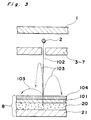
- reference numeral 8 is a screen plate equivalent to a screen 73 of Fig. 1, the screen plate being composed of a glass plate 21, a phosphor 20 to be positioned on it, a metal back (aluminum layer) 101 provided on the phosphor 20, a carbon layer 104 provided on the metal back 101.
- Reference numeral 102 shows electron beams to be generated from the linear cathode 2
- reference numeral 103 is a rearward dispersed electrons (secondary electrons).
- the rearward dispersed electrons 103 are 18% of the electron beams 102 incident in a case of aluminum (atomic number 13) normally used even in the metal back 101.
- the rearward dispersed electrons 103 become 9% of the electron beams 102 incident in the case of carbon (atomic number 6). If a carbon layer 104 is formed on the metal back 101, the generation of the rearward dispersion electrons 103 can be prevented by half, and the contrast ratio is improved twice.
- Fig. 4 is a structural model of a carbon layer forming method.
- phosphor 20 and a metal back 101 are already formed on the internal face of a glass plate 21.
- Carbon liquid 11 with powdered carbon being dissolved in a solvent such as water, alcohol or the like is put into a sprayer 12, is sprayed onto the metal back 101 of the glass plate 21 so as to provide the carbon layer 104. Thereafter, it is burned at approximately 450°C and the face plate is completed as a whole.
- the thickness of the carbon layer 104 can be adjusted by the spraying time or the spraying amount of the sprayer 12. When the carbon layer 104 is too thick, the passing ratio of the electron beams is lowered, thus reducing the brilliance.
- Fig. 6 is a structural model of another carbon layer forming method.
- phosphor 20 and a metal back 101 are already formed on the internal face of a glass plate 21.
- a sufficient amount of carbon powder 13 is prepared and a glass plate 21 is placed above it with the metal back 101 being directed downwards.
- a high voltage of a high tension generator 14 connected with the metal back 101 is applied, and a carbon layer 104 is formed on the metal back 101 by the electric evaporation. Thereafter, it is burned at approximately 450°C and the face plate is be completed as a whole.
- the carbon layer is formed by electric evaporation, a more uniform carbon layer may be obtained than by the spraying in the first method.
- the high-tension voltage to be applied upon the metal back on the face is comparatively low (in a case 15KV or lower), the face where uneven brilliance is not caused may be formed.
- the equal effect may be obtained if the normal temperature solid material which is smaller at the atomic number than aluminum is used.
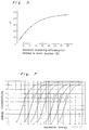
- Fig. 7 is a graph showing the relation of the electron incident energy to the energy transmission factor when the thickness of the metal back 101 is provided as a parameter.
- the metal back 101 is 1000 ⁇ in thickness with an electric potential of 10KV being applied upon it in Fig. 3.
- the electron beams 102 generated from the linear cathode 2 (potential OV) are accelerated by the potential gradient with respect to the metal back 101, and are applied upon the metal back with the incident energy of 10keV.
- the target is aluminum
- 18% of the incident electrons are dispersed as rearward dispersed electrons 103, and the energy of the rearward dispersed electrons 103 becomes approximately 6keV (approximately 60 % of the incident energies).
- the secondary electrons dispersed rearwards rush into the metal back again with an energy of approximately 6keV by the above described potential gradient.
- the energy transmission factor of the incident electrons (10keV) is 92%
- the energy transmission factor of the rearward dispersion electrons (6keV) is 64%. While the brilliance is extremely high, the transmission factor of the rearward dispersed electrons is also high, and the contrast is deteriorated.
- the energy transmission factors of the incident electrons and of the rearward dispersed electrons are respectively 77%, 16%.
- the energy transmission factor (which is proportional to brilliance) of the incident electrons changes from 92% to 77% and the brilliance is also lowered somewhat.
- the energy transmission factor (proportional to halation) of the rearward dispersed electrons is reduced as extremely low from 64% to 16%. Therefore, the brilliance is satisfactory and the contrast is also extremely good.
- the thickness of the metal back 101 is increased extremely, the brilliance is also extremely lowered, so that a proper thickness is demanded.
- the thickness is proper to be 2000 ⁇ or more and 3500 ⁇ or lower when the voltage of the metal back is 10KV. In the case of 9kV, it is proper to be 1500 ⁇ or more and 3000A or lower. In the case of 8KV, it is proper to be 1500 ⁇ or more and 2000 ⁇ or lower.
- the halation may be considerably reduced within some brilliance reduction by the adjustment of the thickness.
Description
Claims (5)
- A flat image display circuit including a flat image display and circuitry having a voltage supply; the flat image display comprisinga vacuum envelope having a face plate (8), a back cell (1) and a plurality of vacuum cells having a potential gradient;a plurality of cathodes (2) disposed within said vacuum envelope for radiating electron beams (102) toward said face plate (8);control electrodes (3 ... 7) for controlling the electron beams (102) radiated from said cathodes (2);a phosphor layer (20) on said face plate (8) and positioned to be irradiated by the electron beams (102) and for emitting light when irradiated by the electron beams; andan aluminum back layer (101) on the face of said phosphor layer (20) towards said cathode (2) for directing light emitted by said phosphor layer (20) to the face of said face plate (8); characterized bysaid image display comprising a uniform layer (104) of material having an atomic number which is smaller than that of aluminum on top of said aluminum back layer (101) and facing said cathodes (2) for reducing the generation of rearward dispersed electrons at the time of irradiation of said phosphor layer (20) by the electron beams (102), this uniform layer being deposited by an electric evaporation process (Fig. 6); said aluminum back layer (101) having a thickness of 1500Å to 3500Å for limiting the transmission factor of rearward dispersed electrons (103) generated at the time of irradiation of the phosphor layer (20) with the electron beams (101) to no more than 30%; andsaid voltage supply applying a voltage of 8KV to 10KV to said back layer (101).
- An image display element in accordance with claim 1,
where the layer (104) of material having an atomic number which is smaller than that of aluminum, consists of a carbon layer. - An image display element in accordance with claim 1 or 2,
wherein for a supply voltage of the aluminum back layer (101) of 10KV the thickness is from 2000Å to 3500Å. - An image display element in accordance with claim 1 or 2,
wherein for a supply voltage of the aluminum back layer (101) of 9KV the thickness is from 1500Å to 3000Å. - An image display element in accordance with claim 1 or 2,
wherein for a supply voltage of the aluminum back layer (101) of 8KV the thickness is from 1500Å to 2000Å.
Applications Claiming Priority (4)
| Application Number | Priority Date | Filing Date | Title |
|---|---|---|---|
| JP6315890A JPH03266339A (en) | 1990-03-14 | 1990-03-14 | Image display element |
| JP63158/90 | 1990-03-14 | ||
| JP7944290 | 1990-03-28 | ||
| JP79442/90 | 1990-03-28 |
Publications (3)
| Publication Number | Publication Date |
|---|---|
| EP0446878A2 EP0446878A2 (en) | 1991-09-18 |
| EP0446878A3 EP0446878A3 (en) | 1992-03-25 |
| EP0446878B1 true EP0446878B1 (en) | 1998-06-03 |
Family
ID=26404244
Family Applications (1)
| Application Number | Title | Priority Date | Filing Date |
|---|---|---|---|
| EP19910103789 Expired - Lifetime EP0446878B1 (en) | 1990-03-14 | 1991-03-13 | Image display element |
Country Status (2)
| Country | Link |
|---|---|
| EP (1) | EP0446878B1 (en) |
| DE (1) | DE69129506T2 (en) |
Families Citing this family (2)
| Publication number | Priority date | Publication date | Assignee | Title |
|---|---|---|---|---|
| KR960016719B1 (en) * | 1993-02-08 | 1996-12-20 | 마쯔시다덴기산교 가부시기가이샤 | Electron beam display and method of manufacturing the same |
| US20010038894A1 (en) * | 2000-03-14 | 2001-11-08 | Minoru Komada | Gas barrier film |
Family Cites Families (3)
| Publication number | Priority date | Publication date | Assignee | Title |
|---|---|---|---|---|
| US3340421A (en) * | 1963-07-31 | 1967-09-05 | Sony Corp | Cathode ray tube having metallic layer of non-uniform thickness |
| US3703401A (en) * | 1970-12-28 | 1972-11-21 | Rca Corp | Method for preparing the viewing-screen structure of a cathode-ray tube |
| GB2120840A (en) * | 1982-05-12 | 1983-12-07 | Philips Electronic Associated | Contrast improvement in vacuum image display devices |
-
1991
- 1991-03-13 EP EP19910103789 patent/EP0446878B1/en not_active Expired - Lifetime
- 1991-03-13 DE DE1991629506 patent/DE69129506T2/en not_active Expired - Fee Related
Also Published As
| Publication number | Publication date |
|---|---|
| EP0446878A3 (en) | 1992-03-25 |
| DE69129506T2 (en) | 1998-10-01 |
| EP0446878A2 (en) | 1991-09-18 |
| DE69129506D1 (en) | 1998-07-09 |
Similar Documents
| Publication | Publication Date | Title |
|---|---|---|
| US4973888A (en) | Image display device | |
| US3657596A (en) | Electron image device having target comprising porous region adjacent conductive layer and outer, denser region | |
| US5489817A (en) | Electron-optical terminal image device based on a cold cathode | |
| US2888513A (en) | Image reproduction system | |
| US4598233A (en) | Color display tube and device having such a tube | |
| US3377492A (en) | Flood gun for storage tubes having a dome-shaped cathode and dome-shaped grid electrodes | |
| US2819380A (en) | Method and apparatus for making apertured masks | |
| EP0446878B1 (en) | Image display element | |
| US2837689A (en) | Post acceleration grid devices | |
| US5639330A (en) | Method of making an image display element | |
| GB1585645A (en) | Gas discharge-electron display device | |
| US3603839A (en) | Color television picture tube of the single electron gun type | |
| US4181870A (en) | Assembly of electron guns having different gamma values | |
| US3819984A (en) | Side-by-side dual gun crt having horizontal deflector plates provided with side shields for correction of geometric distortion | |
| US2967262A (en) | Multi-color display tube | |
| US2856559A (en) | Picture storage tube | |
| US3317782A (en) | Image intensifier storage tube | |
| US2981863A (en) | Storage display system | |
| US2785328A (en) | Storage tube | |
| US4160187A (en) | Post-deflection acceleration crt system | |
| US2930930A (en) | Electronic device | |
| US20050146261A1 (en) | Display device | |
| US2888603A (en) | Color television tube and method for color television | |
| US2227092A (en) | Cathode ray tube | |
| US3519874A (en) | Divided screen display tube for store/non-store information presentation |
Legal Events
| Date | Code | Title | Description |
|---|---|---|---|
| PUAI | Public reference made under article 153(3) epc to a published international application that has entered the european phase |
Free format text: ORIGINAL CODE: 0009012 |
|
| 17P | Request for examination filed |
Effective date: 19910313 |
|
| AK | Designated contracting states |
Kind code of ref document: A2 Designated state(s): DE FR GB NL |
|
| PUAL | Search report despatched |
Free format text: ORIGINAL CODE: 0009013 |
|
| AK | Designated contracting states |
Kind code of ref document: A3 Designated state(s): DE FR GB NL |
|
| 17Q | First examination report despatched |
Effective date: 19931022 |
|
| GRAG | Despatch of communication of intention to grant |
Free format text: ORIGINAL CODE: EPIDOS AGRA |
|
| GRAG | Despatch of communication of intention to grant |
Free format text: ORIGINAL CODE: EPIDOS AGRA |
|
| GRAH | Despatch of communication of intention to grant a patent |
Free format text: ORIGINAL CODE: EPIDOS IGRA |
|
| GRAH | Despatch of communication of intention to grant a patent |
Free format text: ORIGINAL CODE: EPIDOS IGRA |
|
| GRAA | (expected) grant |
Free format text: ORIGINAL CODE: 0009210 |
|
| AK | Designated contracting states |
Kind code of ref document: B1 Designated state(s): DE FR GB NL |
|
| REF | Corresponds to: |
Ref document number: 69129506 Country of ref document: DE Date of ref document: 19980709 |
|
| ET | Fr: translation filed | ||
| PLBE | No opposition filed within time limit |
Free format text: ORIGINAL CODE: 0009261 |
|
| STAA | Information on the status of an ep patent application or granted ep patent |
Free format text: STATUS: NO OPPOSITION FILED WITHIN TIME LIMIT |
|
| 26N | No opposition filed | ||
| REG | Reference to a national code |
Ref country code: GB Ref legal event code: IF02 |
|
| PGFP | Annual fee paid to national office [announced via postgrant information from national office to epo] |
Ref country code: FR Payment date: 20030310 Year of fee payment: 13 |
|
| PGFP | Annual fee paid to national office [announced via postgrant information from national office to epo] |
Ref country code: GB Payment date: 20030312 Year of fee payment: 13 |
|
| PGFP | Annual fee paid to national office [announced via postgrant information from national office to epo] |
Ref country code: DE Payment date: 20030320 Year of fee payment: 13 |
|
| PG25 | Lapsed in a contracting state [announced via postgrant information from national office to epo] |
Ref country code: GB Free format text: LAPSE BECAUSE OF NON-PAYMENT OF DUE FEES Effective date: 20040313 |
|
| PG25 | Lapsed in a contracting state [announced via postgrant information from national office to epo] |
Ref country code: DE Free format text: LAPSE BECAUSE OF NON-PAYMENT OF DUE FEES Effective date: 20041001 |
|
| GBPC | Gb: european patent ceased through non-payment of renewal fee |
Effective date: 20040313 |
|
| PG25 | Lapsed in a contracting state [announced via postgrant information from national office to epo] |
Ref country code: FR Free format text: LAPSE BECAUSE OF NON-PAYMENT OF DUE FEES Effective date: 20041130 |
|
| REG | Reference to a national code |
Ref country code: FR Ref legal event code: ST |
|
| PGFP | Annual fee paid to national office [announced via postgrant information from national office to epo] |
Ref country code: NL Payment date: 20070330 Year of fee payment: 17 |
|
| PG25 | Lapsed in a contracting state [announced via postgrant information from national office to epo] |
Ref country code: NL Free format text: LAPSE BECAUSE OF NON-PAYMENT OF DUE FEES Effective date: 20081001 |
|
| NLV4 | Nl: lapsed or anulled due to non-payment of the annual fee |
Effective date: 20081001 |