EP0446878A2 - Image display element - Google Patents
Image display element Download PDFInfo
- Publication number
- EP0446878A2 EP0446878A2 EP91103789A EP91103789A EP0446878A2 EP 0446878 A2 EP0446878 A2 EP 0446878A2 EP 91103789 A EP91103789 A EP 91103789A EP 91103789 A EP91103789 A EP 91103789A EP 0446878 A2 EP0446878 A2 EP 0446878A2
- Authority
- EP
- European Patent Office
- Prior art keywords
- metal back
- layer
- image display
- display element
- electron beams
- Prior art date
- Legal status (The legal status is an assumption and is not a legal conclusion. Google has not performed a legal analysis and makes no representation as to the accuracy of the status listed.)
- Granted
Links
Images


Classifications
-
- H—ELECTRICITY
- H01—ELECTRIC ELEMENTS
- H01J—ELECTRIC DISCHARGE TUBES OR DISCHARGE LAMPS
- H01J29/00—Details of cathode-ray tubes or of electron-beam tubes of the types covered by group H01J31/00
- H01J29/02—Electrodes; Screens; Mounting, supporting, spacing or insulating thereof
- H01J29/10—Screens on or from which an image or pattern is formed, picked up, converted or stored
- H01J29/18—Luminescent screens
- H01J29/28—Luminescent screens with protective, conductive or reflective layers
Abstract
Description
- The present invention generally relates to a cathode-ray tube for displaying the images by the application, upon the phosphor, of the electrons generated by the cathode within a vacuum cell, and more particularly, to an image display element using a cathode-ray tube which has a potential gradient within the vacuum cell.
- Conventionally, although the Braun tube is mainly used as a display element for a color television image display use, it is impossible to make the conventional Braun tube thinner, because the depth thereof is much longer as compared with the size of the picture face.
- As a plate-shaped display apparatus having the same light emitting principle as that of the Braun tube, the present applicant has been proposed a novel display apparatus of the USA patents Nos. 4,451,846 and USP 4,449,148.
- This is a plate type image display apparatus which may fetch the electron beams from a plurality of linear thermal cathodes, may make the electron beams, controlled by an electron beam control electrode, collide against the fluorescent screen, and may display letters, images and so on.
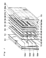
- The plate type image display apparatus is constructed as shown in Fig. 1. In Fig. 1, a
back electrode 51 is adapted to direct into the front face direction theelectron beams 72 to be emitted from a plurality of linear thermal cathodes shown inreference numerals 52a through reference numerals 52d. An electronbeam fetching electrode 53 fetches the electrons by the linearthermal cathode 52a through 52d. Throughholes 62 are provided in theelectrode 53 to let theelectron beams 72 pass through them. Asignal electrode 54 which is provided to apply the video signals is composed of a plurality ofcontrol electrodes 64. Thecontrol electrode 64 has throughholes 63 therein to let theelectron beams 72 pass through it. A first focusingelectrode 55 and a second focusingelectrode 56 are provided to focus theelectron beams 72 in the horizontal and vertical directions. - Through
holes electrodes electron beams 72 to pass through them. Ahorizontal deflection electrode 68 deflects the electron beams in the right, left directions of the picture face, and is composed of one set of comb type ofelectrode electrodes electron beams 72 pass through with the mutual electrodes. Avertical deflection electrode 71 is provided to deflect theelectron beams 72 in the vertical direction of the picture face, and is composed of a set of comb type ofelectrodes electrodes slot 70 with the mutual electrodes to let theelectrode beams 72 to pass through it. A face plate (surface glass cell) 60 has ascreen 73 composed of a three color phosphor layer of red, green, blue, a black stripe layer provided among them, and a metal back layer provided behind them on the inner face thereof. - A
metallic plate 61 made of a back cell, and theface plate 60 constitute a vacuum cell. - But in such a conventional display apparatus as described hereinabove, the rearward dispersed electrons to be generated by the electrons applied upon the metal back layer of the
face plate 60 as the interior of the display element has the potential gradient, instead of equipotential like the conventional Braun tube, are applied again upon the face plate, thus resulting in the largest factor for lowering the contrast ratio. - The above described factors will be described hereinafter again with reference to the drawings.
- Fig. 2 A, B are views showing the internal construction of the Braun tube and the present image display element of the conventional embodiment.
- In the drawings, the portions which are not necessary for illustration are omitted. In the case of the Braun tube a, the
electron beams 82 transmitted from theelectron gun 81 are applied upon themetal back 84 positioned on theface 83. Approximately 80 % of the electron beams pass through themetal back 84 and becomes incident to the fluorescent screen applied upon theface 83 so as to emit the light. - But the
electron beams 82 of approximately remaining 20 % are reflected on themetal back 84 and become the rearward dispersedelectrons 85 so that they are absorbed by afunnel 86 and a shadow mask. This is because the interior of thefunnel 86 is equipotential. Although the approximately 20 % of theelectron beams 82 transmitted from the cathode within theelectrode 88 becomes the rearward dispersedelectrons 85 as in the Braun tube in the case of the present image display element B of the conventional embodiment, the high voltage of approximately 10KV is applied upon the above describedmetal back 84 with theelectrode 88 being provided with respect to approximately 300V. The element has an electrode gradient therein. The rearward dispersedelectrons 85 are applied again upon themetal back 84 on theface 83, and the fluorescent screen except for the place where theelectron beams 82 become incident primarily emits the light, thus reducing the contrast ratio considerably. It is to be noted that themetal back 84 is composed of aluminum layer. - Accordingly, the present invention has been developed with a view to substantially eliminating the above discussed drawbacks inherent in the prior art, and has for its essential object to provide an improved image display element.
- Another important object of the present invention is to provide an improved image display element which is adapted to prevent the reduction in the contrast ratio by the rearward dispersed electrode so as to display the distinct images of good contrast.
- In accomplishing these and other objects, according to the present invention, the carbon layer are formed on the metal back layer on the face plate. The thickness of the metal back layer is adjusted, and the transmission ratio of the transmission factor of the rearward dispersed electrons to be generated at the rush time of the electronic beams is to be restrained at 30% or lower.
- By the above described construction, an image display element is provided where the generation of the rearward dispersed electrons is reduced by approximately half, the light emission of the fluorescent screen except for the location where the electron beams become primarily incident is also reduced by half, the contrast ratio is improved twice.
- These and other objects and features of the present invention will become apparent from the following description taken in conjunction with the preferred embodiments thereof with reference to the accompanying drawings, in which;
- Fig. 1 is an exploded perspective view showing the basic construction of an image display element;
- Fig. 2 A, B are views showing the inner construction of a Braun tube and an image display element;
- Fig. 3 is an approximately side sectional view of an image display element in one embodiment of the present invention;
- Fig. 4 is a structural model showing one example of a carbon layer forming method;
- Fig. 5 is a characteristic graph showing the generation factor of the rearward dispersed electrons with respect to the atomic numeral of a target to which the electron beams become incident;
- Fig. 6 is a structural model view showing the other example of the carbon layer forming method; and
- Fig. 7 is a graph showing the relationship of the electron energy against energy transmission factor with the thickness of the metal back being made parameters.
- Before the description of the present invention proceeds, it is to be noted that like parts are designated by like reference numerals throughout the accompanying drawings.
- One embodiment of the image display element of the present invention will be described hereinafter with reference to the drawings.
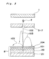
- Fig. 3 is an approximately side sectional view of an image display element of the present invention. Fig. 4 is a structural model showing a forming method of a carbon layer. Fig. 5 is a graph showing the relationship of the generation factor (rearward dispersion coefficient) η of the rearward dispersed electrons with respect to the atomic number Z of an target to which the electron beams become incident.
- In Fig. 3, reference numeral 1 is a back electrode equivalent to the
back electrode 51 of Fig. 1,reference numeral 2 is a linear cathode equivalent to a linear cathode 52 of Fig. 1,reference numerals 3 through 7 are electrode blocks equivalent to abeam fetching electrode 53, asignal electrode 54, a focusingelectrode 55, horizontal · vertical deflecting electrodes 57, 58 of Fig. 1,reference numeral 8 is a screen plate equivalent to ascreen 73 of Fig. 1, the screen plate being composed of aglass plate 21, aphosphor 20 to be positioned on it, a metal back (aluminum layer) 101 provided on thephosphor 20, acarbon layer 104 provided on themetal back 101.Reference numeral 102 shows electron beams to be generated from thelinear cathode 2,reference numeral 103 is a rearward dispersed electrons (secondary electrons). - As clear from Fig. 5, the rearward dispersed
electrons 103 are 18% of theelectron beams 102 to be incident in a case of aluminum (atomic number 13) to be normally used even in themetal back 101. The rearward dispersedelectrons 103 become 9% of theelectron beams 102 to become incident in the case of the carbon (atomic number 6). If thecarbon layer 104 is formed on themetal back 101, the generation of therearward dispersion electrons 103 may be prevented by half, and the contrast ratio may be improved twice. - Fig. 4 is a structural model of the carbon layer forming method. In the drawing, assume that the
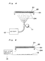
phosphor 20 and themetal back 101 are already formed on the internal face of theglass plate 21. Carbon liquid 11 with powdered carbon being dissolved in a solvent such as water, alcohol or the like is put into asprayer 12, is sprayed onto themetal back 101 of theglass plate 21 so as to thecarbon layer 104. Thereafter, it is burned at approximately 450°C and the face plate is completed as a whole. Here the thickness of thecarbon layer 104 is adjusted by the spraying time or the spraying amount of thesprayer 12. When thecarbon layer 104 is too thick, the passing ratio of the electron beams is lowered, thus reducing the brilliance. Therefore, the carbon layer of approximately 0.3 through 0.4 in the thermal absorption factor is formed this time. - Fig. 6 is a structural model of the carbon layer forming method in a second embodiment of the image display element of the present invention.
- Assume that the
phosphor 20 and the metal back 101 are already formed on the internal face of theglass plate 21. A sufficient amount ofcarbon powder 13 is prepared and aglass plate 21 is placed above it with the metal back 101 being directed downwards. Apply the high voltage with ahigh tension generator 14 being connected with the metal back 101, and thecarbon layer 104 is formed on the metal back 101 by the electric evaporation. Thereafter, it is burned at approximately 450°C and the face plate may be completed as a whole. - When the carbon layer is formed by the electric evaporation, the more uniform carbon layer may be obtained than by the spraying in the first embodiment. When the high-tension voltage to be applied upon the metal back on the face is comparatively low (in a case 15KV or lower), the face where uneven brilliance is not caused may be formed.
- A third embodiment of the present invention will be described hereinafter.
- Silicon resin is provided in the thickness of 2 microns on the full face of the resin film of approximately several tens of microns as a mold releasing layer. The carbon film is formed with spraying, electric evaporating or the like on the mold releasing layer so as to obtain the carbon layer forming sheet. The carbon layer forming sheet is transferred under pressure adherence on the metal back layer on the face plate, is burned at approximately 450°C to complete the face plate as a whole.
- By the formation of the carbon layer through the above described transferring operation, the carbon layer forming sheet may be kept prepared in advance. The pressure adherence transferring operation has only to be effected at the face plate completing step. The simplification of the step may be effected.
- Although the carbon is used in the present embodiment, the equal effect may be obtained if the normal temperature solid material which is smaller at the atomic number than aluminum is used.
- A method of setting the thickness of the metal back 101 will be described with reference to the drawings. Fig. 7 is a graph showing the relation of the electron incident energy to the energy transmission factor when the thickness of the metal back 101 is provided as parameters.
- Assume that the metal back 101 is 1000Å in thickness with the electric potential of 10KV being applied upon it in Fig. 3. In this case, the
electron beams 102 generated from the linear cathode 2 (potential OV) are accelerated by the potential gradient with respect to the metal back 101, and are applied upon the metal back with the incident energy of 10keV. When the target is aluminum, the incident 18% is dispersed rearwards as rearward dispersedelectrons 103, and the energies of the rearward dispersedelectrons 103 become approximately 6keV (approximately 60 % of the incident energies). The secondary electrons dispersed rearwards rushes into the metal back again by the energies of approximately 6keV by the above described potential gradient. When the thickness of the metal back 101 is 1000Å, the energy transmission factor of the incident electrons (10keV) is 92%, the energy transmission factor of the rearward dispersion electrons (6keV) is 64%. Therefore, it is undesirable that the brilliance is extremely high, the transmission factor of the rearward dispersed electrons is also high, and the contrast is deteriorated. Assume that the thickness of the metal back is made 2000Å, the energy transmission factors of the incident electrons, the rearward dispersed electrons are respectively 77%, 16%. When the thickness of the metal back 101 is made 1000Å → 2000Å, the energy transmission factor (which is proportional to brilliance) of the incident electrons becomes 92% - 77% and the brilliance is also lowered somewhat. But the energy transmission factor (proportional to halation) of the rearward dispersed electrons is reduced as extremely low as 64% → 16%. Therefore, the brilliance is satisfactory and the contrast is also extremely good. But when the thickness of the metal back increases extremely, the brilliance is lowered large, so that the proper thickness is demanded. By the experiment, it has been found out that the balancing is provided in the brilliance and the contrast if the energy transmission factor of the rearward dispersed electrons is 30% or lower. On the basis of it, the thickness is proper to be 2000Å or more and 3500Å or lower when the voltage of the metal back is 10KV. In the case of 9kV, it is proper to be 1500Å or more and 3000A or lower. In the case of 8KV, it is proper to be 1500Å or more and 2000Å or lower. - As described hereinabove, the halation may be considerably reduced within some brilliance reduction by the adjustment of the thickness.
- Although the present invention has been fully described by way of example with reference to the accompanying drawings, it is to be noted here that various changes and modifications will be apparent to those skilled in the art. Therefore, unless otherwise such changes and modifications depart from the scope of the present invention, they should be construed as included therein.
Claims (7)
- An image display element comprising a vacuum envelope having a face plate and a back cell, a cathode disposed within the vacuum envelope, a control electrode for controlling the electron beams radiated from the cathode, a hosphor layer positioned on the face plate and adapted to emit the light by the application of the electron beams, a metal back layer positioned on the phosphor layer and adapted to bring the light emission of the phosphor to the front face by the mirror face effect, a carbon layer positioned on the metal back layer to reduce the generation of the rearward dispersed electrons.
- An image display element described in accordance with the claim 1, where the formation of the carbon layer is effected on the electric evaporation.
- An image display element described in accordance with the claim 1, where the carbon layer formed sheet with the carbon film being formed on the mold releasing support member is transferred on the metal back layer on the face plate, the carbon layer is formed by the peeling off of the support member.
- An image display element comprising a vacuum envelope having a face plate and a back cell, a cathode disposed within the vacuum envelope, a control electrode for controlling the electron beams radiated from the cathode, a phosphor layer positioned on the face plate and adapted to emit the light by the application of the electron beams, a metal back layer positioned on the phosphor layer and adapted to bring the light emission of the phosphor to the front face by the mirror face effect, the metal back layer is made of aluminum layer, with the thickness thereof being set to restrain the transmission factor of the rearward dispersed electron beams to be generated at the rush time of the electron beams at 30% or lower.
- An image display element described in accordance with the claim 4, where the voltage of the metal back layer on the face plate is 10Kv, the thickness is 2000Å or more and 3500Å or lower.
- An image display element described in accordance with the claim 4, where the voltage of the metal back layer on the face plate is 9KV, the thickness is 1500Å or more and 3000Å or lower.
- An image display element described in accordance with the claim 4, where the voltage of the metal back layer on the face plate is 8KV, the thickness is 1500A or more and 2000Å or lower.
Applications Claiming Priority (4)
| Application Number | Priority Date | Filing Date | Title |
|---|---|---|---|
| JP63158/90 | 1990-03-14 | ||
| JP6315890A JPH03266339A (en) | 1990-03-14 | 1990-03-14 | Image display element |
| JP7944290 | 1990-03-28 | ||
| JP79442/90 | 1990-03-28 |
Publications (3)
| Publication Number | Publication Date |
|---|---|
| EP0446878A2 true EP0446878A2 (en) | 1991-09-18 |
| EP0446878A3 EP0446878A3 (en) | 1992-03-25 |
| EP0446878B1 EP0446878B1 (en) | 1998-06-03 |
Family
ID=26404244
Family Applications (1)
| Application Number | Title | Priority Date | Filing Date |
|---|---|---|---|
| EP19910103789 Expired - Lifetime EP0446878B1 (en) | 1990-03-14 | 1991-03-13 | Image display element |
Country Status (2)
| Country | Link |
|---|---|
| EP (1) | EP0446878B1 (en) |
| DE (1) | DE69129506T2 (en) |
Cited By (2)
| Publication number | Priority date | Publication date | Assignee | Title |
|---|---|---|---|---|
| EP0610872A2 (en) * | 1993-02-08 | 1994-08-17 | Matsushita Electric Industrial Co., Ltd. | Electron beam display device and production thereof |
| EP1134073A1 (en) * | 2000-03-14 | 2001-09-19 | Dai Nippon Printing Co., Ltd. | Gas barrier film |
Citations (3)
| Publication number | Priority date | Publication date | Assignee | Title |
|---|---|---|---|---|
| DE1281588B (en) * | 1963-07-31 | 1968-10-31 | Sony Corp | Cathode ray tube |
| DE2164174A1 (en) * | 1970-12-28 | 1972-07-06 | Rca Corp | A method of applying a carbon layer on a light-reflecting metal layer covering the phosphor layer on the faceplate portion of a cathode ray tube |
| GB2120840A (en) * | 1982-05-12 | 1983-12-07 | Philips Electronic Associated | Contrast improvement in vacuum image display devices |
-
1991
- 1991-03-13 EP EP19910103789 patent/EP0446878B1/en not_active Expired - Lifetime
- 1991-03-13 DE DE1991629506 patent/DE69129506T2/en not_active Expired - Fee Related
Patent Citations (3)
| Publication number | Priority date | Publication date | Assignee | Title |
|---|---|---|---|---|
| DE1281588B (en) * | 1963-07-31 | 1968-10-31 | Sony Corp | Cathode ray tube |
| DE2164174A1 (en) * | 1970-12-28 | 1972-07-06 | Rca Corp | A method of applying a carbon layer on a light-reflecting metal layer covering the phosphor layer on the faceplate portion of a cathode ray tube |
| GB2120840A (en) * | 1982-05-12 | 1983-12-07 | Philips Electronic Associated | Contrast improvement in vacuum image display devices |
Cited By (6)
| Publication number | Priority date | Publication date | Assignee | Title |
|---|---|---|---|---|
| EP0610872A2 (en) * | 1993-02-08 | 1994-08-17 | Matsushita Electric Industrial Co., Ltd. | Electron beam display device and production thereof |
| EP0610872A3 (en) * | 1993-02-08 | 1994-10-12 | Matsushita Electric Ind Co Ltd | Electron beam display device and production thereof. |
| US5451835A (en) * | 1993-02-08 | 1995-09-19 | Matsushita Electric Industrial Co., Ltd. | Electron beam display device and production thereof |
| EP1134073A1 (en) * | 2000-03-14 | 2001-09-19 | Dai Nippon Printing Co., Ltd. | Gas barrier film |
| EP1522403A2 (en) * | 2000-03-14 | 2005-04-13 | Dai Nippon Printing Co., Ltd. | Gas barrier film |
| EP1522403A3 (en) * | 2000-03-14 | 2008-10-22 | Dai Nippon Printing Co., Ltd. | Gas barrier film |
Also Published As
| Publication number | Publication date |
|---|---|
| EP0446878B1 (en) | 1998-06-03 |
| DE69129506D1 (en) | 1998-07-09 |
| EP0446878A3 (en) | 1992-03-25 |
| DE69129506T2 (en) | 1998-10-01 |
Similar Documents
| Publication | Publication Date | Title |
|---|---|---|
| US2280191A (en) | Cathode-ray signal-reproducing unit | |
| CA2319395A1 (en) | A fed crt having various control and focusing electrodes along with horizontal and vertical deflectors | |
| US2888513A (en) | Image reproduction system | |
| US2837689A (en) | Post acceleration grid devices | |
| US3377492A (en) | Flood gun for storage tubes having a dome-shaped cathode and dome-shaped grid electrodes | |
| US5639330A (en) | Method of making an image display element | |
| EP0446878A2 (en) | Image display element | |
| US2970219A (en) | Use of thin film field emitters in luminographs and image intensifiers | |
| US3028521A (en) | Image-reproducting device | |
| US3819984A (en) | Side-by-side dual gun crt having horizontal deflector plates provided with side shields for correction of geometric distortion | |
| US6288482B1 (en) | Color cathode ray tube with reduced drive voltage | |
| US4181870A (en) | Assembly of electron guns having different gamma values | |
| US2785328A (en) | Storage tube | |
| US3317782A (en) | Image intensifier storage tube | |
| US20050146261A1 (en) | Display device | |
| US2914696A (en) | Electron beam device | |
| US3304462A (en) | Single gun storage tube with target emission sustained by electric field | |
| US2227092A (en) | Cathode ray tube | |
| US4160187A (en) | Post-deflection acceleration crt system | |
| US4065695A (en) | Cathode ray tube screen having charge-retaining layer apertured in registration with color elements | |
| GB791486A (en) | Improvements in or relating to cathode-ray tubes | |
| US2805359A (en) | Television pick-up tubes and television apparatus incorporating the same | |
| US6369512B1 (en) | Dual beam projection tube and electron lens therefor | |
| US3484862A (en) | Colour kinescopes | |
| US4900978A (en) | Electron gun having blackened grids used in-line type color CRT, and color CRT using the same |
Legal Events
| Date | Code | Title | Description |
|---|---|---|---|
| PUAI | Public reference made under article 153(3) epc to a published international application that has entered the european phase |
Free format text: ORIGINAL CODE: 0009012 |
|
| 17P | Request for examination filed |
Effective date: 19910313 |
|
| AK | Designated contracting states |
Kind code of ref document: A2 Designated state(s): DE FR GB NL |
|
| PUAL | Search report despatched |
Free format text: ORIGINAL CODE: 0009013 |
|
| AK | Designated contracting states |
Kind code of ref document: A3 Designated state(s): DE FR GB NL |
|
| 17Q | First examination report despatched |
Effective date: 19931022 |
|
| GRAG | Despatch of communication of intention to grant |
Free format text: ORIGINAL CODE: EPIDOS AGRA |
|
| GRAG | Despatch of communication of intention to grant |
Free format text: ORIGINAL CODE: EPIDOS AGRA |
|
| GRAH | Despatch of communication of intention to grant a patent |
Free format text: ORIGINAL CODE: EPIDOS IGRA |
|
| GRAH | Despatch of communication of intention to grant a patent |
Free format text: ORIGINAL CODE: EPIDOS IGRA |
|
| GRAA | (expected) grant |
Free format text: ORIGINAL CODE: 0009210 |
|
| AK | Designated contracting states |
Kind code of ref document: B1 Designated state(s): DE FR GB NL |
|
| REF | Corresponds to: |
Ref document number: 69129506 Country of ref document: DE Date of ref document: 19980709 |
|
| ET | Fr: translation filed | ||
| PLBE | No opposition filed within time limit |
Free format text: ORIGINAL CODE: 0009261 |
|
| STAA | Information on the status of an ep patent application or granted ep patent |
Free format text: STATUS: NO OPPOSITION FILED WITHIN TIME LIMIT |
|
| 26N | No opposition filed | ||
| REG | Reference to a national code |
Ref country code: GB Ref legal event code: IF02 |
|
| PGFP | Annual fee paid to national office [announced via postgrant information from national office to epo] |
Ref country code: FR Payment date: 20030310 Year of fee payment: 13 |
|
| PGFP | Annual fee paid to national office [announced via postgrant information from national office to epo] |
Ref country code: GB Payment date: 20030312 Year of fee payment: 13 |
|
| PGFP | Annual fee paid to national office [announced via postgrant information from national office to epo] |
Ref country code: DE Payment date: 20030320 Year of fee payment: 13 |
|
| PG25 | Lapsed in a contracting state [announced via postgrant information from national office to epo] |
Ref country code: GB Free format text: LAPSE BECAUSE OF NON-PAYMENT OF DUE FEES Effective date: 20040313 |
|
| PG25 | Lapsed in a contracting state [announced via postgrant information from national office to epo] |
Ref country code: DE Free format text: LAPSE BECAUSE OF NON-PAYMENT OF DUE FEES Effective date: 20041001 |
|
| GBPC | Gb: european patent ceased through non-payment of renewal fee |
Effective date: 20040313 |
|
| PG25 | Lapsed in a contracting state [announced via postgrant information from national office to epo] |
Ref country code: FR Free format text: LAPSE BECAUSE OF NON-PAYMENT OF DUE FEES Effective date: 20041130 |
|
| REG | Reference to a national code |
Ref country code: FR Ref legal event code: ST |
|
| PGFP | Annual fee paid to national office [announced via postgrant information from national office to epo] |
Ref country code: NL Payment date: 20070330 Year of fee payment: 17 |
|
| PG25 | Lapsed in a contracting state [announced via postgrant information from national office to epo] |
Ref country code: NL Free format text: LAPSE BECAUSE OF NON-PAYMENT OF DUE FEES Effective date: 20081001 |
|
| NLV4 | Nl: lapsed or anulled due to non-payment of the annual fee |
Effective date: 20081001 |