EP0446829B1 - Light emitter array diagnostic apparatus - Google Patents
Light emitter array diagnostic apparatus Download PDFInfo
- Publication number
- EP0446829B1 EP0446829B1 EP91103678A EP91103678A EP0446829B1 EP 0446829 B1 EP0446829 B1 EP 0446829B1 EP 91103678 A EP91103678 A EP 91103678A EP 91103678 A EP91103678 A EP 91103678A EP 0446829 B1 EP0446829 B1 EP 0446829B1
- Authority
- EP
- European Patent Office
- Prior art keywords
- light emitter
- emitter array
- light
- unit
- photo detector
- Prior art date
- Legal status (The legal status is an assumption and is not a legal conclusion. Google has not performed a legal analysis and makes no representation as to the accuracy of the status listed.)
- Expired - Lifetime
Links
- 238000003745 diagnosis Methods 0.000 claims description 26
- 230000003287 optical effect Effects 0.000 claims description 20
- 238000001514 detection method Methods 0.000 description 40
- 238000006243 chemical reaction Methods 0.000 description 8
- 238000012986 modification Methods 0.000 description 4
- 230000004048 modification Effects 0.000 description 4
- 230000002411 adverse Effects 0.000 description 3
- 230000003247 decreasing effect Effects 0.000 description 3
- 238000000034 method Methods 0.000 description 3
- 239000002131 composite material Substances 0.000 description 2
- 230000000694 effects Effects 0.000 description 2
- 230000035945 sensitivity Effects 0.000 description 2
- 230000001419 dependent effect Effects 0.000 description 1
- 238000005401 electroluminescence Methods 0.000 description 1
- 230000001771 impaired effect Effects 0.000 description 1
- 239000012212 insulator Substances 0.000 description 1
- 239000004973 liquid crystal related substance Substances 0.000 description 1
- 238000001454 recorded image Methods 0.000 description 1
Images


Classifications
-
- B—PERFORMING OPERATIONS; TRANSPORTING
- B41—PRINTING; LINING MACHINES; TYPEWRITERS; STAMPS
- B41J—TYPEWRITERS; SELECTIVE PRINTING MECHANISMS, i.e. MECHANISMS PRINTING OTHERWISE THAN FROM A FORME; CORRECTION OF TYPOGRAPHICAL ERRORS
- B41J2/00—Typewriters or selective printing mechanisms characterised by the printing or marking process for which they are designed
- B41J2/435—Typewriters or selective printing mechanisms characterised by the printing or marking process for which they are designed characterised by selective application of radiation to a printing material or impression-transfer material
- B41J2/44—Typewriters or selective printing mechanisms characterised by the printing or marking process for which they are designed characterised by selective application of radiation to a printing material or impression-transfer material using single radiation source per colour, e.g. lighting beams or shutter arrangements
-
- B—PERFORMING OPERATIONS; TRANSPORTING
- B41—PRINTING; LINING MACHINES; TYPEWRITERS; STAMPS
- B41J—TYPEWRITERS; SELECTIVE PRINTING MECHANISMS, i.e. MECHANISMS PRINTING OTHERWISE THAN FROM A FORME; CORRECTION OF TYPOGRAPHICAL ERRORS
- B41J2/00—Typewriters or selective printing mechanisms characterised by the printing or marking process for which they are designed
- B41J2/435—Typewriters or selective printing mechanisms characterised by the printing or marking process for which they are designed characterised by selective application of radiation to a printing material or impression-transfer material
- B41J2/447—Typewriters or selective printing mechanisms characterised by the printing or marking process for which they are designed characterised by selective application of radiation to a printing material or impression-transfer material using arrays of radiation sources
- B41J2/45—Typewriters or selective printing mechanisms characterised by the printing or marking process for which they are designed characterised by selective application of radiation to a printing material or impression-transfer material using arrays of radiation sources using light-emitting diode [LED] or laser arrays
Definitions
- This invention relates to an optical recording apparatus such as an optical printer whose light source is a light emitter array, and more particularly to a diagnostic apparatus for diagnosing whether or not light emitter elements forming the light emitter array in the optical printer are satisfactorily normally emitting light.
- a conventional optical printer having a light emitting diode (LED) array as its light source has a structure as schematically shown in Fig. 10.
- data to be recorded is supplied from a host computer 100 to an LED array printer 200.
- This LED array printer 200 is generally composed of a driver circuit 201, an LED array 202, an image focusing lines array 203 and a photoconductive drum 204.
- the data is supplied in a digital form so as to selectively cause emission of light from corresponding LED elements (not shown) in the LED array 202.
- data corresponding to one line is sequentially supplied from the host computer 100 to cover all of the LED elements arrayed to form the LED array 202.
- the data supplied from the host computer 100 is subjected to serial-parallel conversion in the driver circuit 201 so as to selectively cause emission of light from the LED elements in the LED array 202 according to the data supplied from the host computer 100.
- Light emitted from the energized LED elements among those forming the LED array 202 is focused by the focusing lens array 203 to form a dot image on the photoconductive drum 204.
- Such a manner of line sequential scanning for causing emission of light from selected LED elements is continued so as to sequentially form a dot image on the photoconductive drum 204 being rotated.
- character, pattern or like images are recorded on the photoconductive drum 204.
- the dot images formed on the photoconductive drum 204 are then transfer printed on a sheet of paper by a method such as an electrostatic recording method.
- JP-A-61-264361 cited above does not refer to the case where any one of the LED elements in the LED array does not emit light due to, for example, disconnection of its power supply lead and does not also refer to the detection of the quantity of light emitted from each of the LED elements.
- a light emitter array diagnostic apparatus which comprises a light emitter array unit, a photo detector means disposed in the emission space of the light emitter array opposite to the light emitting surface of the light emitter array and divided into a plurality of photo detector units electrically connected in series, a check data generator unit supplying check data to the light emitter array unit divided into a plurality of groups corresponding to the respective photo detector units at the time of emission diagnosis so as to sequentially select at least one light emitter element from each of the groups and to cause simultaneous emission of light from the selected light emitter elements and a diagnostic unit sequentially comparing a reference signal with a signal appearing across output terminals of the series-connected photo detector units at the time of the emission diagnosis, and, when the level of the output signal of the series-connected photo detector units is lower than that of the reference signal, diagnosis that at least one of the light emitter elements which should simultaneously emit light is faulty.
- an output terminal is provided for each of the photo detector units in lieu of electrically connecting all of the photo detector units in series, and a signal appearing from each of the output terminals is compared with the reference signal.
- an output terminal is provided for each of the photo detector units in lieu of electrically connecting all of the photo detector units in series, and the sum of the signals appearing from all of the output terminals is compared with the reference signal.
- odd-numbered ones and even-numbered ones of the photo detector units are separately connected in series respectively in lieu of electrically connecting all of the photo detector units in series, and odd-numbered output terminals and even-numbered output terminals are separately provided so that signals appearing from these output terminals are diagnosed in a time series mode.
- the photo detector means is not divided into the plural photo detector units and remains in a single unit.
- the single photo detector unit is replaced by two photo detector units disposed at different positions.
- the photo detector means is divided into the plural photo detector units each of which receives light emitted from at least one light emitter element in the corresponding group of the light emitter unit so that the emission diagnosis for all of the light emitter elements forming the light emitter array can be attained at a high speed.
- the photo detector means is not divided but remains in the single unit, so that, by merely comparing the signal appearing from the single output terminal of the photo detector unit, the emission diagnosis for all of the light emitter elements forming the light emitter array can be attained at a high speed.
- Fig. 1 is a diagrammatic view showing the structure of a first embodiment of the light emitter array diagnostic apparatus according to the present invention.
- Fig. 2 is a schematic perspective view of the first embodiment of the present invention shown in Fig. 1.
- Figs. 3A and 3B show two forms respectively of the photo diode arrangement employed in the present invention.
- Figs. 4, 5, 6 and 7 show a second, a third, a fourth and a fifth embodiment respectively of the present invention.
- Fig. 8 shows a partial modification of the fifth embodiment of the present invention shown in Fig. 7.
- Figs. 9A and 9B show two forms respectively of the diagnostic timing according to the present invention.
- Fig. 10 is a diagrammatic view generally illustrating the prior art concerning the present invention.
- Fig. 1 shows a first embodiment of the light emitter array diagnostic apparatus according to the present invention.
- the light emitter array diagnostic apparatus comprises a check data generator 1 acting as a check data supply unit, a driver circuit 2, an LED array 3 which is a light emitter array unit, a faulty LED element detector 4 acting as a diagnostic unit, a plurality of photo diodes 41, 42, 43, ..., 4n, each of which is a photo detector unit, an amplifier 5, a comparator 6, a decision circuit 6a, an image data input terminal IN, and a switching unit S1.
- the LED array 3 consisting of several-thousand LED elements is divided into a plurality of groups 31, 32, 33, ..., 3n each having the same number of LED elements.
- the LED array 3 is divided into such equally-sized groups for the sake of convenience only, and this manner of grouping does not in any way limit the arrangement of the LED elements forming the LED array 3.
- the check data generator 1 generates check data so as to diagnose as to whether or not any one of the LED elements forming the LED array 3 is faulty and fail to normally emit light. It is necessary to detect whether or not each of the LED elements forming the LED array 3 emits light by actuating LED elements.
- the check data generator 1 supplies check data in each scanning step so that at least one LED element in each of the groups 31, 32, 33, ..., 3n forming the LED array 3 is energized to emit light in response to the check data.
- one LED element in each of the groups 31, 32, 33, ..., 3n that is, a total of n LED elements are simultaneously energized to emit light.
- the LED elements different from those energized in the preceding scanning step in the respective groups are simultaneously energized to emit light.
- the check data generator 1 repeatedly generates the check data a plurality of times until all of the LED elements constituting the LED array 3 have been energized to emit light.
- the check data is such that a plurality of LED elements are scanned by a scanning signal to cause simultaneous emission of light from these LED elements. Practical examples of the manner of scanning and the check data will now be described.
- the number of the LED elements can be expressed as (m x n), where m represents the number of columns, and n represents the number of rows. That is, these LED elements are grouped into m groups each including n LED elements in the LED array 3.
- the LED element numbers belonging to the first to the m-th group respectively are as follows: According to the above manner of grouping, the LED elements having the following numbers are scanned in the first to the n-th scanning steps, respectively: Thus, according to the above manner of scanning, the LED elements numbered (1, 1), (2, 1), ..., (m, 1) are selected at the time of the first scanning, and these m LED elements are simultaneously energized to emit light in response to the check data. After this first scanning, the second scanning starts, and, in the second scanning, the LED elements numbered (1, 2), (2, 2), ..., (m, 2) are selected and simultaneously energized to emit light in response to the check data. Thereafter, the sequential scanning continues until the n-th scanning is completed. In this manner, all of the LED elements are energized to emit light for the purpose of the emission diagnosis.
- the driver circuit 2 is composed of an (m x n)-bit register and drive means.
- the check data having a pattern as described in (2) is supplied from the check data generator 1, the check data is subjected to serial-parallel conversion in the driver circuit 2, so that the LED elements selected by the emission data are simultaneously energized to emit light.
- the emission data for causing simultaneous emission of light from LED elements E1, E2, E3, ..., E n located at the left ends of the respective groups 31, 32, 33, ..., 3n of the LED array 3 is supplied to the driver circuit 2 at the time of certain scanning.
- the emission data is subjected to the serial-parallel conversion in the driver circuit 2 so as to simultaneously energize the LED elements E1, E2, E3, ..., E n .
- E1, E2, E3, ..., E n As a result, light outputs L1, L2, L3, ..., L n appear from these LED elements, respectively.
- the photoelectric transducer connected to the faulty LED element detector 4 has such a structure that the plural photo diodes 41, 42, 43, ..., 4n each having a short length corresponding to the associated group of the LED array 3 (which diodes will be referred to hereinafter as short-size photo diodes) are electrically connected in cascade to extend along the full length of the LED array 3.
- Each of these short-size photo diodes 41, 42, 43, ..., 4n is disposed at the position where it can receive light emitted from whatever LED element belongs to the associated groups 31, 32, 33, ..., 3n of the LED array 3.
- Each of these short-size photo diodes 41, 42, 43, ..., 4n has a light receiving surface having a wide area capable of receiving light emitted from any one of the LED elements belonging to the associated groups 31, 32, 33, ..., 3n of the LED array 3.
- Such a short-size photo diode can be equivalently replaced by a voltaic cell when the diode is conducting, and it can be replaced by an insulator when the diode is not conducting. Therefore, when any one of the cascade-connected photo diode corresponding to any one of the groups 31, 32, 33, ..., 3n of the LED array 3 is not receiving emission, no photovoltage appears across output terminals 41A and 41B of the cascade connection.
- Fig. 2 is a schematic perspective view of the first embodiment of the present invention, and, in Fig. 2, the LED array 3, the short-size photo diodes 41 to 4n, the focusing lens array 203 and the photoconductive drum 204 are emphasized.
- the short-size photo diodes 41 to 4n are disposed in close proximity and in parallel to the focusing lens array 203.
- the short-size photo diode 41 receives light emitted from the LED elements belonging to the group 31, and the short-size photo diode 42 receives light emitted from the LED elements belonging to the group 32.
- Fig. 3A is a schematic sectional view taken along the line IIIA - IIIA in Fig. 1.
- Fig. 3B is a sectional view of another form corresponding to Fig. 3A.
- Each of Figs. 3A and 3B shows that, among the plural LED elements, a specific one supplied with the check data is emitting light.
- Fig. 3A shows that the light output from the LED array 3 passes through an optical path 8 shown by the dotted lines to be transmitted through the focusing lens array 203.
- Fig. 3B shows that the light output passes through a similar optical path 8 to be transmitted through a focusing lens array 203.
- the reference numeral 10 designates a light shielding case which is not shown in Figs.
- the short-size photo diode 40 is disposed in the light shielding case 10 at a position outside of the optical path 8 along which the light output from the LED array 3 generally passes to be transmitted through the focusing lens array 203. That is, the short-size photo diode 40 is disposed at a position where it receives the light output 9 from the LED array 3.
- short-size photo diode 401 corresponding to odd-numbered group (for example, groups 31, 33) of LED array 3 and short-size photo diode 402 corresponding to even-numbered group (for example, group 32, 34) of LED array 3 are disposed on both sides respectively of the optical path 8 when viewed from the focusing lens array 203.
- the response time of each of the short-size photo diodes 41, 42, 43, ..., 4n shown in Fig. 1 is generally greatly dependent on its junction capacity.
- C is the junction capacity of each of these short-size photo diodes 41, 42, 43, ..., 4n.
- the overall electrostatic capacity when viewed from the detection output terminals 41A and 41B is given by C/n, where n is the number of the photo diodes.
- the short-size photo diodes 41, 42, 43, ..., 4n receive the light outputs L1, L2, L3, ..., L n of the same light quantity from the LED elements E1, E2, E3, ..., E n respectively. Therefore, photovoltages of the same quantity are induced in the respective short-size photo diodes 41, 42, 43, ..., 4n, and a detection resistor Rd detects the sum of the photovoltages.
- the amplifier 5 has input resistors R1, R2 and a resistor R3 connected across its input and output terminals. The voltage detected by the detection resistor Rd is amplified by the amplifier 5 up to a level of about several volts.
- the LED array 3 includes a faulty LED element
- the overall photovoltage is correspondingly decreased to decrease the voltage detected by the detection resistor Rd.
- the comparator 6 is provided for the purpose of this identification. Also, when any one of the LED elements does not emit light, the short-size photo diode associated with the faulty LED element is not active, and a zero output appears across its output terminals.
- the output of the photo electric transducer is applied to one input terminal D of the comparator 6, while a reference voltage obtained from dividing a source voltage by resistors R4 and R5 is applied to the other input terminal REF of the comparator 6.
- This reference voltage is set at a value between a minimum voltage (an absolute value) detected when all of plural LED elements simultaneously energized to emit light are normal and a maximum voltage (an absolute value) detected when any one of these LED elements is faulty. Therefore, when one or more of these LED elements are faulty, the detected voltage is lower than the reference voltage, and a binary output signal having a logic level "H" appears at the output terminal OUT of the comparator 6. On the other hand, when all of the LED elements are normal, a binary output signal having a logic level "L” appears at the output terminal OUT of the comparator 6.
- the faulty LED element detection carried out in the manner described above by the use of the check data generated from the check data generator 1 is commonly performed separately from the image recording operation. Therefore, the switching unit S1 is provided so as to switch over the image data supplied from the input terminal IN and the check data supplied from the check data generator 1.
- the operation sequence is programed so that, before the image recording mode is started by turning on the power supply or between the preceding image recording operation and the next, the switching unit S1 is switched to supply the check data to the driver circuit 2 so as to start the faulty LED element detection mode.
- the period of time required for the emission diagnosis of all the LED elements constituting the LED array can be greatly shortened.
- the short-size photo diodes 41, 42, 43, ..., 4n are connected in cascade, the electrostatic capacity when viewed from the detection output terminals becomes small in an inversely proportional relation to the number of the short-size photo diodes, so that the response time of the outputs of the LED elements simultaneously energized in one scanning step can be accelerated. Therefore, because the period of time required for one scanning step simultaneously energizing the plural LED elements can be shortened, the period of time required for the emission diagnosis of all the LED elements constituting the LED array 3 can be further accelerated.
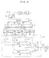
- Fig. 4 shows a second embodiment of the present invention, and, in Fig. 4, like reference numerals are used to designate like parts appearing in Fig. 1.
- the apparatus comprises a check data generator 1, a driver circuit 2, an LED array 3, a faulty LED element detector 4, a plurality of short-size photo diodes 41 to 4n, a pair of amplifiers 5 disposed in the faulty LED element detector 4, a decision circuit 6a, an image data input terminal IN, a switching unit S1, and another switching unit S2 disposed in the detector 4.
- the LED array 3 is divided into a plurality of groups 31, 32, 33, ..., 3n. However, this grouping implies no hardware limitation in the structure of the LED array 3.
- the faulty LED element detector 4 is associated with a photoelectric transducer which is composed of the plural short-size photo diodes 41, 42, 43, ..., 4n arranged to correspond to the respective groups 31, 32, 33, ..., 3n of the LED array 3.
- the short-size photo diodes located at positions where they do not receive light outputs from the LED element belonging to the other groups are grouped to form a plurality of groups G1 and G2 corresponding to the short-size photo diodes 41, 43 and 42, 44 as shown in Fig. 4. That is, the even-numbered short-size photo diodes 41, 43 and the odd-numbered short-size photo diodes 42, 44 are grouped into two groups.
- the short-size photo diodes 41, 43 belonging to the group G1 are electrically connected in cascade, and the output from this group G1 is applied to one of two detection resistors Rd.
- the short-size photo diodes 42, 44 belonging to the group G2 are electrically connected in cascade, and the output from this group G2 is applied to the other detection resistor Rd.
- the short size photo diodes 41 to 4n so grouped cover the full length of the LED array 3 so that the light output from whatever LED element can be photoelectrically converted.
- the short-size photo diodes 41 to 4n may be disposed on one side only of the optical path when viewed from the focusing lens array 203 as shown in Fig. 3A, or their groups G1 and G2 may be disposed on the left and right sides respectively of the optical path when viewed from the focusing lens array 203 as shown in Fig. 3B.
- the check data generator 1 generates check data for detecting whether or not the LED array 3 includes a faulty LED element, and this emission diagnostic operation is carried out separately from the image recording operation.
- the check data generator 1 generates the check data before the image recording mode is started by turning on the power supply or between the preceding image recording operation and the next.
- the switching unit S1 controls the data flow so that the check data can be supplied separately from image data supplied to the input terminal IN.
- the operation of this second embodiment is the same as that of the first embodiment in that the check data generator 1 repeats the scanning a plurality of times until all of the LED elements in the LED array 3 have been energized to emit light.
- the scanning with the check data is such that a plurality of LED elements belonging to different groups corresponding to one photo diode group, for example, the LED elements E1 and E3 in the respective groups 31 and 33 corresponding to the photo diode group G1 are simultaneously energized in one scanning step, and such a manner of scanning is repeated until all of the LED elements in the groups corresponding to the photo diode group G1 have been energized to emit light. Then, the similar manner of scanning is repeated for the LED elements belonging to the groups corresponding to the photo diode group G2, so that all of the LED elements in the LED array 3 are energized to emit light.
- the number of the groups in the LED array 3 is increased, the number of the LED elements simultaneously scanned in one scanning step is increased. Therefore, the number of the scanning steps is decreased in an inversely proportional relation to the number of the groups, and the period of time required for the emission diagnosis can be correspondingly shortened.
- the check data supplied to the drive circuit 2 in each scanning step is subjected to serial-parallel conversion, so that the LED elements are simultaneously energized to emit light according to the check data.
- the LED elements E1 and E3 generate their light outputs L1 and L3 respectively in one scanning step.
- the short-size photo diodes 41 and 43 belonging to the photo diode group G1 receive the light outputs L1 and L3 from the LED elements E1 and E3 respectively, and the associated detection resistor Rd detects the sum of the photovoltages. While the LED elements belonging to the groups corresponding to the photo diode group G1 are being diagnosed, the detection signal is output to the exterior through the switching unit S2.
- the diagnostic sequence is such that, as soon as the emission diagnosis for the LED elements belonging to the groups corresponding to the photo diode group G2 is started, the switching unit S2 switches over the detection route.
- the associated short-size photo diode When any one of the LED elements scanned for the purpose of emission diagnosis is faulty, the associated short-size photo diode does not generate its output, and its internal impedance becomes high. As a result, any substantial output does not appear from the associated detection resistor Rd even when the remaining short-size photo diodes connected in cascade receive normal light outputs. That is, when the plural LED elements simultaneosuly energized to emit light do not include a faulty one, each of the photo diodes has a low internal impedance, and a high output is generated from each of the photo diodes in the photo diode group.
- the electrostatic capacity of the short-size photo diode group when viewed from detection output terminals is the combined value of the junction capacities of the short-size photo diodes connected in cascade and becomes small in an inversely proportional relation to the number of the photo diodes. Therefore, the detection signal response is quick, and the scanning can be made at a high speed.
- the amplifiers 5 amplify the detection signals up to a level of about several volts so that the output signal of the faulty LED element detector 4 can be easily handled in the digital circuit 6a connected thereto.
- a faulty LED element detector is connected to groups of short-size photo diodes 41, 42, 43, ..., 4n connected in cascade to have a decreased effective electrostatic capacity, so as to operate at a high speed. Because such a detector is used to diagnose emission from a plurality of LED elements simultaneosuly energized, the period of time required for the emission diagnosis of all of the LED elements in the LED array 3 can be greatly shortened.
- the emission diagnosis in which a plurality of LED elements are simultaneously energized to emit light, the light outputs from these LED elements are photoelectrically converted by the cascade-connected short-size photo diodes 41, 42, 43, ..., 4n, and the faulty LED element detector generates a binary signal having a logic level indicating whether a specific LED element is faulty or not. Therefore, the second embodiment exhibits the merit that the structure of the circuit is simplified.
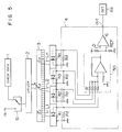
- Fig. 5 shows a third embodiment of the present invention, and, in Fig. 5, like reference numerals are used to designate like parts appearing in Fig. 1.
- the apparatus comprises a check data generator 1, a driver circuit 2, an LED array 3, a faulty LED element detector 4, a plurality of short-size photo diodes 41, 42, 43, ..., 4n, an adder 50, a comparator 6, a decision circuit 6a an image data input terminal IN, and a switching unit S1.
- the check data generator 1 generates check data for simultaneously energizing a plurality of LED elements in the LED array 3.
- the check data generated in one scanning step is such that, for example, LED elements E1, E2, ..., E n are simultaneously energized to emit their light outputs L1, L2, ..., L n respectively.
- a plurality of other LED elements are simultaneously energized.
- the check data generator 1 repeatedly generates check data so as to simultaneously energize a predetermined plurality of LED elements in each scanning step until all of the LED elements are energized to emit light.
- the switching unit S1 controls the data flow so that the check data can be supplied separately from image data supplied to the input terminal IN.
- the operation sequence is programed so that, before the image recording mode is started by turning on the power supply or between the preceding image recording operation and the next, the switching unit S1 is switched to supply the check data so as to diagnose the emission from the LED elements.
- the check data supplied to the driver circuit 2 in each scanning step is subjected to serial-parallel conversion, so that the LED elements are simultaneously energized to emit light according to the check data.
- the plural short-size photo diodes 41, 42, 43, ..., 4n apply their outputs representing the result of photoelectric conversion to the faulty LED element detector 4.
- These short-size photo diodes 41, 42, 43, ..., 4n are arranged on one line on one side only of the optical path when viewed from the focusing lens array 203 as shown in Fig. 3A or arranged in a zig-zag relation straddling the optical path when viewed from the focusing lens array 203 as shown in Fig. 3B, so that they can receive the light outputs from whatever LED elements constituting the LED array 3.
- these short-size photo diodes 41, 42, 43, ..., 4n are equivalent to a full-size photo diode.
- the photovoltages generated from these short-size photo diodes 41, 42, 43, ..., 4n are applied across associated detection resistors Rd respectively to appear as detection signals which are applied to the adder 50 through associated input resistor R respectively.
- the adder 50 generates its output voltage proportional to the sum of the light outputs from normal ones of the plural LED elements simultaneously energized to emit light.
- the output voltage of the adder 50 represents the sum of the light outputs from the LED elements simultaneously energized in the LED array 3 in one scanning step, and the function of the short-size photo diode group is equivalent to that of the full-size photo diode.
- the detection signal response speed is determined by the junction capacity of the photo diodes.
- the present invention is advantageous in that the period of time required for each scanning operation can be correspondingly shortened.
- the output voltage of the adder 50 is applied to one input terminal D of the comparator 6.
- a reference voltage is applied to the other input terminal REF of the comparator 6.
- This reference voltage is set at a value between a minimum voltage (an absolute value) detected when all of plural LED elements simultaneously energized to emit light are normal and a maximum voltage (an absolute value) detected when any one of these LED elements is faulty. Therefore, when one or more LED elements are faulty, the detected voltage is lower than the reference voltage, and a binary output signal having a logic level "H” appears at the output terminal OUT of the comparator 6. On the other hand, when all of the LED elements are normal, a binary output signal having a logic level "L” appears at the output terminal OUT of the comparator 6.
- the provision of a plurality of short-size photo diodes 41, 42, 43, ..., 4n can accelerate the response of the photoelectric transducer, and a plurality of LED elements can be simultaneously diagnosed.
- the period of time required for the emission diagnosis for all of the LED elements can be shortened.
- the outputs from the photo detector units which may not have the same or uniform sensitivity are summed by an adder, so that an adverse effect attributable to a fluctuation of the sensitivities of the individual photo detector units can be minimized.
- Fig. 6 shows a fourth embodiment of the present invention, and, in Fig. 6, like reference numerals are used to designate like parts appearing in Fig. 1.
- the apparatus comprises a check data generator 1, a driver circuit 2, an LED array 3, a faulty LED element detector 4, a photo diode 41, an amplifier 5, a comparator 6, a decision circuit 6a, a switching unit S1, and an image data input terminal IN.
- the manners of generation of check data control of the data flow sequence and energization of LED elements in the LED array 3 are the same as those in the third embodiment described above. That is, when the check data generator 1 is actuated by turning on the power supply in each scanning step, a predetermined plurality of LED elements different from those energized in the preceding step are simultaneously energized to emit light.
- the single photo diode 41 receiving the light outputs from these LED elements is electrically connected to the faulty LED element detector 4 which diagnoses whether or not any one of the LED elements is faulty.
- This photo diode 41 has a full-size light receiving area so that it can receive the light output from any one of the LED elements in the LED array 3.
- This photo diode 41 is disposed at a position as shown in Fig. 3A. That is, the photo diode 41 is disposed at a position which is close to the LED array 3 but outside of the optical path 8 of light emitted from the LED array 3 to pass through the focusing lens array 203.
- the photo diode 41 generates a photovoltage proportional to the number of the light-emitting LED elements, and this photovoltage is applied across a detection resistor Rd to appear as a detection signal.
- the function and operation of the amplifier 5 and the comparator 6 are entirely the same as those described with reference to Fig. 1 showing the first embodiment. Therefore, when any one of the LED elements simultaneosuly energized to emit light is faulty, an error signal having a logic level "H" appears at the output terminal OUT of the comparator 6.
- a plurality of LED elements are simultaneously energized to emit light in each scanning step, so that all of the LED elements can be diagnosed within a short period of time.
- Fig. 7 shows a fifth embodiment of the present invention, and, in Fig. 7, like reference numerals are used to designate like parts appearing in Fig. 6.
- the apparatus comprises a check data generator 1, a driver circuit 2, an image data input terminal IN, a switching unit S1, an LED array 3, a faulty LED element detector 4, photo diodes 41, 42, an amplifier 5, an adder 50, a comparator 6, and a decision circuit 6a.
- this fifth embodiment is entirely the same as that of the third and fourth embodiments described above in that check data generated from the check data generator 1 and supplied through the switching unit S1 and the driver circuit 2 simultaneously energize a predetermined plurality of different LED elements in each scanning step, and such a scanning operation is repeated until all of the LED elements are energized to emit light.
- the two photo diodes 41 and 42 receiving the light outputs from the plural LED elements in each scanning step are electrically connected to the faulty LED element detector 4 which diagnoses whether or not any one of these LED elements is faulty.
- Each of these photo diodes 41 and 42 has a full size corresponding to the size of the LED array 3 as in the case of the photo diode 41 used in the fourth embodiment described above.
- These photo diode 41 corresponding to odd-numbered group of LED array 3 and photo diode 42 corresponding to even-numbered group of LED array 3 are disposed at positions close to the LED array 3 on both sides respectively of the optical path 8 when viewed from the focusing lens array 203 as shown in Fig. 3B.
- these photo diodes 41 and 42 are disposed outside of the optical path 8 of light emitted from the LED array 3 to path through the focusing lens array 203, and receive the light emitted from the LED array 3.
- These two full-size photo diodes 41 and 42 are electrically connected in cascade to apply their outputs across a detection resistor Rd. Because of the above arrangement, the light outputs from the individual LED elements are received by the two full-size photo diodes 41 and 42, and the outputs of the photo diodes are summed. Therefore, the detection output voltage of the detection resistor Rd is two times as high as that obtained when the single photo diode is provided, so that the output voltage is substantially freed from the adverse effect of a noise signal.
- the composite junction capacity of the photo diodes 41 and 42 connected in cascade is equivalently halved when viewed from the detection output terminals, so that the response speed for the light outputs from the LED elements becomes high.
- the detection output signal from the detection resistor Rd is amplified up to a level of about several volts by the amplifier 5, and the amplified detection output signal from the amplifier 5 is applied to the comparator 6.
- the comparator 6 When any one of the plural LED elements simultaneously energized is faulty, the comparator 6 generates an error signal as in the case of the first and fourth embodiments described above.
- the photo detector units 41 and 42 can be comprised of a plurality of photo diodes thereof, respectively.
- the photo diodes 41 and 42 can be connected with any types as shown in Fig. 1, Fig. 4 and Fig. 5.
- Fig. 8 shows a modification of the faulty LED element detector 4 shown in Fig. 7.
- the full-size photo diodes 41 and 42 disposed on both sides respectively of the optical path 8 when viewed from the focusing lens array 203 are electrically connected to the respective detection resistors Rd, and the detection output signals from these detection resistors Rd are summed by an adder 50.
- the light outputs from the individual LED elements are received by the two full-size photo diodes 41 and 42, and the outputs of these photo diodes are summed.
- the level of the detection output voltage from the adder 50 is two times as high as that obtained when the single photo diode is provided, so that the detection output signal is easily distinguished from a noise signal.
- the response speed of the detection output signal in response to the light outputs from the LED elements is the same as that obtained when the single photo diode is provided. Thus, the response speed is not lowered regardless of the increase in detection output voltage.
- a plurality of LED elements are simultaneosuly energized for the emission diagnosis in each scanning step, so that the period of time required for the emission diagnosis of all of the LED elements in the LED array 3 can be shortened. Further, because the light outputs from the LED elements are received by two full-size photo diodes to be summed thereby doubling the detected light quantity. Therefore, the emission diagnosis can be carried out without being adversely effected by noise.
- its recording apparatus includes an LED array as a light source.
- the light emitter array used in the present invention is in no way limited to the LED array 3 and may be any one of for example, an electroluminescence element array, a liquid crystal shutter array and a laser array.
- a photoconductor device such as an image sensor may be used as a photo detector in lieu of the photo diode.
- the LED array is divided into a plurality of groups in the order of from one end thereof, it is apparent that the LED array may be randomly divided into such groups without any limitation in the positions of the groups.
- Figs. 9A and 9B show two forms of the diagnostic timing, that is, the timing for switching the switching unit S1.
- Fig. 9A shows that the emission diagnosis is performed between preceding image printing (or character printing) operation and the next.
- Fig. 9B shows that the emission diagnosis is performed at the starting time and ending time only of the image printing (or character printing) operation.
- a full-size photo diode is provided for an LED array or a plurality of short-size photo diodes which constitute an equivalent full-size photo diode are provided for an LED array so as to receive light simultaneously emitted from a plurality of LED elements and to photoelectrically convert the light outputs, so that the plural LED elements can be subjected to the emission diagnosis at a time. Therefore, the period of time required for the emission diagnosis of all of the LED elements constituting the LED array can be greatly shortened. Further, when the plural photo diodes are connected in cascade, the composite electrostatic capacity becomes small, so that the photo response speed of the detection output signal is accelerated. Therefore, the plural LED elements can be scanned at a high speed in each scanning step for the emission diagnosis, so that the period of time required for the emission diagnosis of all of the LED elements constituting the LED array can be greatly shortened.
Landscapes
- Physics & Mathematics (AREA)
- Optics & Photonics (AREA)
- Health & Medical Sciences (AREA)
- General Health & Medical Sciences (AREA)
- Toxicology (AREA)
- Printers Or Recording Devices Using Electromagnetic And Radiation Means (AREA)
- Led Devices (AREA)
- Led Device Packages (AREA)
- Accessory Devices And Overall Control Thereof (AREA)
- Dot-Matrix Printers And Others (AREA)
- Exposure Or Original Feeding In Electrophotography (AREA)
- Facsimile Heads (AREA)
Description
- This invention relates to an optical recording apparatus such as an optical printer whose light source is a light emitter array, and more particularly to a diagnostic apparatus for diagnosing whether or not light emitter elements forming the light emitter array in the optical printer are satisfactorily normally emitting light.
- A conventional optical printer having a light emitting diode (LED) array as its light source has a structure as schematically shown in Fig. 10. Referring to Fig. 10, data to be recorded is supplied from a
host computer 100 to anLED array printer 200. ThisLED array printer 200 is generally composed of adriver circuit 201, anLED array 202, an image focusinglines array 203 and aphotoconductive drum 204. The data is supplied in a digital form so as to selectively cause emission of light from corresponding LED elements (not shown) in theLED array 202. In this case, data corresponding to one line is sequentially supplied from thehost computer 100 to cover all of the LED elements arrayed to form theLED array 202. The data supplied from thehost computer 100 is subjected to serial-parallel conversion in thedriver circuit 201 so as to selectively cause emission of light from the LED elements in theLED array 202 according to the data supplied from thehost computer 100. Light emitted from the energized LED elements among those forming theLED array 202 is focused by the focusinglens array 203 to form a dot image on thephotoconductive drum 204. Such a manner of line sequential scanning for causing emission of light from selected LED elements is continued so as to sequentially form a dot image on thephotoconductive drum 204 being rotated. Thus, character, pattern or like images are recorded on thephotoconductive drum 204. The dot images formed on thephotoconductive drum 204 are then transfer printed on a sheet of paper by a method such as an electrostatic recording method. - When the luminance of any one or more of the LED elements forming the
LED array 202 is subject to a variation, it leads to the problem that the optical density of the recorded image is not maintained constant, and the image quality will be greatly impaired or degraded. Such a variation in the luminance of emission is attributable to various factors including the temperature, corruption and secular variation. An attempt to deal with such a problem is made in, for example, JP-A-61-264361 which discloses that the quantity of light emitted from an LED array is detected by a luminous power sensor, and the period of time of emission from the LED array is controlled on the basis of the result of luminous power detection so as to maintain constant the quantity of light emitted from the LED array. - However, JP-A-61-264361 cited above does not refer to the case where any one of the LED elements in the LED array does not emit light due to, for example, disconnection of its power supply lead and does not also refer to the detection of the quantity of light emitted from each of the LED elements.
- When any one of the LED elements becomes faulty, the corresponding portion of the dot image drops out. In such a case, the problem is more serious than the case of a non-uniform image density distribution in that the information will sometimes be incorrectly recorded. Therefore, it is necessary to diagnose whether or not any one of the LED elements in the LED array becomes faulty in the state in which the LED array is incorporated in a printer. This problem is addressed by EP-A-0 297 603, wherein a diagnostic apparatus according to the preamble portion of
claim 1 is described. In this apparatus, the LED elements are checked by causing them to shine one by one, each element in turn, detecting the light emitted by any of the elements and processing the detection signals so as to provide data representing functional characteristics of each of the elements. - It is an object of the present invention to provide a light emitter array diagnostic apparatus which can detect a faulty light emitter element, if any, by diagnosing all of light emitter elements in a light emitter array within a short period of time.
- This object is achieved by a diagnostic apparatus according to
claim 1. - In one embodiment of the present invention there is provided a light emitter array diagnostic apparatus which comprises a light emitter array unit, a photo detector means disposed in the emission space of the light emitter array opposite to the light emitting surface of the light emitter array and divided into a plurality of photo detector units electrically connected in series, a check data generator unit supplying check data to the light emitter array unit divided into a plurality of groups corresponding to the respective photo detector units at the time of emission diagnosis so as to sequentially select at least one light emitter element from each of the groups and to cause simultaneous emission of light from the selected light emitter elements and a diagnostic unit sequentially comparing a reference signal with a signal appearing across output terminals of the series-connected photo detector units at the time of the emission diagnosis, and, when the level of the output signal of the series-connected photo detector units is lower than that of the reference signal, diagnosis that at least one of the light emitter elements which should simultaneously emit light is faulty.
- In another embodiment of the present invention, an output terminal is provided for each of the photo detector units in lieu of electrically connecting all of the photo detector units in series, and a signal appearing from each of the output terminals is compared with the reference signal.
- In still another embodiment of the present invention, an output terminal is provided for each of the photo detector units in lieu of electrically connecting all of the photo detector units in series, and the sum of the signals appearing from all of the output terminals is compared with the reference signal.
- In yet another embodiment of the present invention, odd-numbered ones and even-numbered ones of the photo detector units are separately connected in series respectively in lieu of electrically connecting all of the photo detector units in series, and odd-numbered output terminals and even-numbered output terminals are separately provided so that signals appearing from these output terminals are diagnosed in a time series mode.
- In a further embodiment of the present invention, the photo detector means is not divided into the plural photo detector units and remains in a single unit.
- In a still further embodiment of the present invention, the single photo detector unit is replaced by two photo detector units disposed at different positions.
- According to one embodiment of the present invention, the photo detector means is divided into the plural photo detector units each of which receives light emitted from at least one light emitter element in the corresponding group of the light emitter unit so that the emission diagnosis for all of the light emitter elements forming the light emitter array can be attained at a high speed.
- Further, according to another embodiment of the present invention, the photo detector means is not divided but remains in the single unit, so that, by merely comparing the signal appearing from the single output terminal of the photo detector unit, the emission diagnosis for all of the light emitter elements forming the light emitter array can be attained at a high speed.
- Fig. 1 is a diagrammatic view showing the structure of a first embodiment of the light emitter array diagnostic apparatus according to the present invention.
- Fig. 2 is a schematic perspective view of the first embodiment of the present invention shown in Fig. 1.
- Figs. 3A and 3B show two forms respectively of the photo diode arrangement employed in the present invention.
- Figs. 4, 5, 6 and 7 show a second, a third, a fourth and a fifth embodiment respectively of the present invention.
- Fig. 8 shows a partial modification of the fifth embodiment of the present invention shown in Fig. 7.
- Figs. 9A and 9B show two forms respectively of the diagnostic timing according to the present invention.
- Fig. 10 is a diagrammatic view generally illustrating the prior art concerning the present invention.
- Preferred embodiments of the present invention will now be described in detail with reference to the accompanying drawings.
- Fig. 1 shows a first embodiment of the light emitter array diagnostic apparatus according to the present invention. Referring to Fig. 1, the light emitter array diagnostic apparatus comprises a
check data generator 1 acting as a check data supply unit, adriver circuit 2, anLED array 3 which is a light emitter array unit, a faultyLED element detector 4 acting as a diagnostic unit, a plurality ofphoto diodes amplifier 5, acomparator 6, adecision circuit 6a, an image data input terminal IN, and a switching unit S1. - The
LED array 3 consisting of several-thousand LED elements is divided into a plurality ofgroups LED array 3 is divided into such equally-sized groups for the sake of convenience only, and this manner of grouping does not in any way limit the arrangement of the LED elements forming theLED array 3. Thecheck data generator 1 generates check data so as to diagnose as to whether or not any one of the LED elements forming theLED array 3 is faulty and fail to normally emit light. It is necessary to detect whether or not each of the LED elements forming theLED array 3 emits light by actuating LED elements. However, when most of the many LED elements forming theLED array 3 are simultaneously emitting light, it is impossible to identify one or more LED elements which are faulty and fail to normally emit light. Therefore, it is necessary to limit the number of the LED elements which are simultaneously energized and to divide the emission detection into a plurality of scanning steps. In the first embodiment of the present invention, thecheck data generator 1 supplies check data in each scanning step so that at least one LED element in each of thegroups LED array 3 is energized to emit light in response to the check data. Thus, in one scanning step, one LED element in each of thegroups check data generator 1 repeatedly generates the check data a plurality of times until all of the LED elements constituting theLED array 3 have been energized to emit light. - The check data is such that a plurality of LED elements are scanned by a scanning signal to cause simultaneous emission of light from these LED elements. Practical examples of the manner of scanning and the check data will now be described.
- For simplicity of description, all of the linearly arranged LED elements are numbered (1, 1), (1, 2), ..., (2, 1), (2, 2), ..., (m, n) in the order of from the leftmost one in Fig. 1. Therefore, the number of the LED elements can be expressed as (m x n), where m represents the number of columns, and n represents the number of rows. That is, these LED elements are grouped into m groups each including n LED elements in the
LED array 3. Therefore, the LED element numbers belonging to the first to the m-th group respectively are as follows: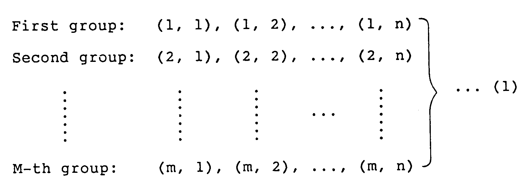
According to the above manner of grouping, the LED elements having the following numbers are scanned in the first to the n-th scanning steps, respectively:
Thus, according to the above manner of scanning, the LED elements numbered (1, 1), (2, 1), ..., (m, 1) are selected at the time of the first scanning, and these m LED elements are simultaneously energized to emit light in response to the check data. After this first scanning, the second scanning starts, and, in the second scanning, the LED elements numbered (1, 2), (2, 2), ..., (m, 2) are selected and simultaneously energized to emit light in response to the check data. Thereafter, the sequential scanning continues until the n-th scanning is completed. In this manner, all of the LED elements are energized to emit light for the purpose of the emission diagnosis. - There are various forms for supplying the check data, as described below.
- (1) In one form, the check data representing the element numbers (the addresses) of the LED elements to be simultaneously scanned is sequentially generated from the
check data generator 1. In this case, the check data representing the element numbers (the addresses) of the LED elements numbered (1, 1), (2, 1), ..., (m, 1) is sequentially generated in the first scanning. At this time, emission data "1" for the diagnostic purpose is added to the element numbers (the addresses) of the LED elements to be scanned. The same applies to the second and succeeding scanning. - (2) The emission data "1" is directly generated to indicate each of the element numbers of the LED elements to be simultaneosuly scanned. For example, at the time of the first scanning for the LED elements numbered (1, 1), (2, 1), ..., (m, 1), the
check data generator 1 generates data "1", but generates data "0" for the remaining LED elements having the other element numbers, as follows:
check data generator 1 is as follows:
check data generator 1 continuously generates similar check data patterns until the end of the n-th scanning. - (3) The
check data generator 1 generates and supplies check data of 1-bit only to thedriver circuit 2, and a separate scanning circuit carries out the scanning according to the scanning mode given by the expression (2). - (4) There are various other manners of supplying the check data. In such a case too, it is the essential requirement that the LED elements in the
LED array 3 are to be scanned according to the scanning mode given by the expression (2). For this purpose, both thecheck data generator 1 and thedriver circuit 2 may have structures different from those shown in Fig. 1. - The
driver circuit 2 is composed of an (m x n)-bit register and drive means. When the check data having a pattern as described in (2) is supplied from thecheck data generator 1, the check data is subjected to serial-parallel conversion in thedriver circuit 2, so that the LED elements selected by the emission data are simultaneously energized to emit light. Suppose, for example, that the emission data for causing simultaneous emission of light from LED elements E₁, E₂, E₃, ..., En located at the left ends of therespective groups LED array 3 is supplied to thedriver circuit 2 at the time of certain scanning. The emission data is subjected to the serial-parallel conversion in thedriver circuit 2 so as to simultaneously energize the LED elements E₁, E₂, E₃, ..., En. As a result, light outputs L₁, L₂, L₃, ..., Ln appear from these LED elements, respectively. - The photoelectric transducer connected to the faulty
LED element detector 4 has such a structure that theplural photo diodes LED array 3. Each of these short-size photo diodes groups LED array 3. - Each of these short-
size photo diodes groups LED array 3. Such a short-size photo diode can be equivalently replaced by a voltaic cell when the diode is conducting, and it can be replaced by an insulator when the diode is not conducting. Therefore, when any one of the cascade-connected photo diode corresponding to any one of thegroups LED array 3 is not receiving emission, no photovoltage appears across output terminals 41A and 41B of the cascade connection. - Fig. 2 is a schematic perspective view of the first embodiment of the present invention, and, in Fig. 2, the
LED array 3, the short-size photo diodes 41 to 4n, the focusinglens array 203 and thephotoconductive drum 204 are emphasized. Referring to Fig. 2, the short-size photo diodes 41 to 4n are disposed in close proximity and in parallel to the focusinglens array 203. The short-size photo diode 41 receives light emitted from the LED elements belonging to thegroup 31, and the short-size photo diode 42 receives light emitted from the LED elements belonging to thegroup 32. The same applies to the relation between the remaining photo diodes and the remaining groups. - Fig. 3A is a schematic sectional view taken along the line IIIA - IIIA in Fig. 1. Fig. 3B is a sectional view of another form corresponding to Fig. 3A. Each of Figs. 3A and 3B shows that, among the plural LED elements, a specific one supplied with the check data is emitting light. Fig. 3A shows that the light output from the
LED array 3 passes through an optical path 8 shown by the dotted lines to be transmitted through the focusinglens array 203. Similarly, Fig. 3B shows that the light output passes through a similar optical path 8 to be transmitted through a focusinglens array 203. In each of Figs. 3A and 3B, thereference numeral 10 designates a light shielding case which is not shown in Figs. 1 and 2. In Fig. 3A, the short-size photo diode 40 is disposed in thelight shielding case 10 at a position outside of the optical path 8 along which the light output from theLED array 3 generally passes to be transmitted through the focusinglens array 203. That is, the short-size photo diode 40 is disposed at a position where it receives the light output 9 from theLED array 3. In the case of Fig. 3B, short-size photo diode 401 corresponding to odd-numbered group (for example,groups 31, 33) ofLED array 3 and short-size photo diode 402 corresponding to even-numbered group (for example,group 32, 34) ofLED array 3 are disposed on both sides respectively of the optical path 8 when viewed from the focusinglens array 203. - The response time of each of the short-
size photo diodes size photo diodes photo diodes LED array 3 does not include any faulty LED element, the short-size photo diodes size photo diodes amplifier 5 has input resistors R₁, R₂ and a resistor R₃ connected across its input and output terminals. The voltage detected by the detection resistor Rd is amplified by theamplifier 5 up to a level of about several volts. - When now the
LED array 3 includes a faulty LED element, the overall photovoltage is correspondingly decreased to decrease the voltage detected by the detection resistor Rd. In order to generate an error signal, when any one of the LED elements simultaneously energized to emit light at the time of each scanning step is faulty, it is necessary to identify the faulty LED element on the basis of the detected voltage variation attributable to the faulty LED element. Thecomparator 6 is provided for the purpose of this identification. Also, when any one of the LED elements does not emit light, the short-size photo diode associated with the faulty LED element is not active, and a zero output appears across its output terminals. Even when that LED element does not emit light, light emitted from the LED element belonging to the group other than the group to which the faulty LED element belongs, may be incident upon the short-size photo diode associated with the faulty LED element. However, in this case, the quantity of the incident light is small, so that the emission diagnosis can be made according to the same process as that carried out to deal with the presence of a faulty LED element. - The output of the photo electric transducer is applied to one input terminal D of the
comparator 6, while a reference voltage obtained from dividing a source voltage by resistors R₄ and R₅ is applied to the other input terminal REF of thecomparator 6. This reference voltage is set at a value between a minimum voltage (an absolute value) detected when all of plural LED elements simultaneously energized to emit light are normal and a maximum voltage (an absolute value) detected when any one of these LED elements is faulty. Therefore, when one or more of these LED elements are faulty, the detected voltage is lower than the reference voltage, and a binary output signal having a logic level "H" appears at the output terminal OUT of thecomparator 6. On the other hand, when all of the LED elements are normal, a binary output signal having a logic level "L" appears at the output terminal OUT of thecomparator 6. - The faulty LED element detection carried out in the manner described above by the use of the check data generated from the
check data generator 1 is commonly performed separately from the image recording operation. Therefore, the switching unit S1 is provided so as to switch over the image data supplied from the input terminal IN and the check data supplied from thecheck data generator 1. Thus, the operation sequence is programed so that, before the image recording mode is started by turning on the power supply or between the preceding image recording operation and the next, the switching unit S1 is switched to supply the check data to thedriver circuit 2 so as to start the faulty LED element detection mode. - According to the first embodiment of the present invention, whether any one of a plurality of LED elements is faulty or not, can be diagnosed by one scanning step simultaneously energizing these LED elements. Therefore, the period of time required for the emission diagnosis of all the LED elements constituting the LED array can be greatly shortened. Further, because the short-
size photo diodes LED array 3 can be further accelerated. - Fig. 4 shows a second embodiment of the present invention, and, in Fig. 4, like reference numerals are used to designate like parts appearing in Fig. 1. Referring to big. 4, the apparatus comprises a
check data generator 1, adriver circuit 2, anLED array 3, a faultyLED element detector 4, a plurality of short-size photo diodes 41 to 4n, a pair ofamplifiers 5 disposed in the faultyLED element detector 4, adecision circuit 6a, an image data input terminal IN, a switching unit S1, and another switching unit S2 disposed in thedetector 4. As in the case of the first embodiment, theLED array 3 is divided into a plurality ofgroups LED array 3. - The faulty
LED element detector 4 is associated with a photoelectric transducer which is composed of the plural short-size photo diodes respective groups LED array 3. The short-size photo diodes located at positions where they do not receive light outputs from the LED element belonging to the other groups are grouped to form a plurality of groups G1 and G2 corresponding to the short-size photo diodes size photo diodes size photo diodes 42, 44 are grouped into two groups. The short-size photo diodes size photo diodes 42, 44 belonging to the group G2 are electrically connected in cascade, and the output from this group G2 is applied to the other detection resistor Rd. The shortsize photo diodes 41 to 4n so grouped cover the full length of theLED array 3 so that the light output from whatever LED element can be photoelectrically converted. The short-size photo diodes 41 to 4n may be disposed on one side only of the optical path when viewed from the focusinglens array 203 as shown in Fig. 3A, or their groups G1 and G2 may be disposed on the left and right sides respectively of the optical path when viewed from the focusinglens array 203 as shown in Fig. 3B. - The
check data generator 1 generates check data for detecting whether or not theLED array 3 includes a faulty LED element, and this emission diagnostic operation is carried out separately from the image recording operation. As in the case of the first embodiment, thecheck data generator 1 generates the check data before the image recording mode is started by turning on the power supply or between the preceding image recording operation and the next. The switching unit S1 controls the data flow so that the check data can be supplied separately from image data supplied to the input terminal IN. The operation of this second embodiment is the same as that of the first embodiment in that thecheck data generator 1 repeats the scanning a plurality of times until all of the LED elements in theLED array 3 have been energized to emit light. The scanning with the check data is such that a plurality of LED elements belonging to different groups corresponding to one photo diode group, for example, the LED elements E₁ and E₃ in therespective groups LED array 3 are energized to emit light. When the number of the groups in theLED array 3 is increased, the number of the LED elements simultaneously scanned in one scanning step is increased. Therefore, the number of the scanning steps is decreased in an inversely proportional relation to the number of the groups, and the period of time required for the emission diagnosis can be correspondingly shortened. - As in the case of the first embodiment, the check data supplied to the
drive circuit 2 in each scanning step is subjected to serial-parallel conversion, so that the LED elements are simultaneously energized to emit light according to the check data. For example, the LED elements E₁ and E₃ generate their light outputs L₁ and L₃ respectively in one scanning step. - The short-
size photo diodes - When any one of the LED elements scanned for the purpose of emission diagnosis is faulty, the associated short-size photo diode does not generate its output, and its internal impedance becomes high. As a result, any substantial output does not appear from the associated detection resistor Rd even when the remaining short-size photo diodes connected in cascade receive normal light outputs. That is, when the plural LED elements simultaneosuly energized to emit light do not include a faulty one, each of the photo diodes has a low internal impedance, and a high output is generated from each of the photo diodes in the photo diode group. On the other hand, when any one of the LED elements is faulty, its internal impedance is high, and no output appears from that photo diode in the photo diode group. This manner of photoelectric conversion is very convenient for the diagnosis for detecting the presence or absence of a faulty LED element. Thus, according to the above manner of photoelectric conversion, a binary signal representing the presence or absence of a faulty LED element appears at an output terminal OUT regardless of the number of faulty LED elements among the plural LED elements simultaneously energized.
- The electrostatic capacity of the short-size photo diode group when viewed from detection output terminals is the combined value of the junction capacities of the short-size photo diodes connected in cascade and becomes small in an inversely proportional relation to the number of the photo diodes. Therefore, the detection signal response is quick, and the scanning can be made at a high speed.
- The
amplifiers 5 amplify the detection signals up to a level of about several volts so that the output signal of the faultyLED element detector 4 can be easily handled in thedigital circuit 6a connected thereto. - According to the second embodiment of the present invention described above, a faulty LED element detector is connected to groups of short-
size photo diodes LED array 3 can be greatly shortened. - Further, in the emission diagnosis in which a plurality of LED elements are simultaneously energized to emit light, the light outputs from these LED elements are photoelectrically converted by the cascade-connected short-
size photo diodes - Fig. 5 shows a third embodiment of the present invention, and, in Fig. 5, like reference numerals are used to designate like parts appearing in Fig. 1. Referring to Fig. 5, the apparatus comprises a
check data generator 1, adriver circuit 2, anLED array 3, a faultyLED element detector 4, a plurality of short-size photo diodes adder 50, acomparator 6, adecision circuit 6a an image data input terminal IN, and a switching unit S1. - The
check data generator 1 generates check data for simultaneously energizing a plurality of LED elements in theLED array 3. The check data generated in one scanning step is such that, for example, LED elements E₁, E₂, ..., En are simultaneously energized to emit their light outputs L₁, L₂, ..., Ln respectively. In the next scanning step, a plurality of other LED elements, the number of which is the same as that energized in the preceding scanning step, are simultaneously energized. In the manner described above, thecheck data generator 1 repeatedly generates check data so as to simultaneously energize a predetermined plurality of LED elements in each scanning step until all of the LED elements are energized to emit light. The switching unit S1 controls the data flow so that the check data can be supplied separately from image data supplied to the input terminal IN. As in the case of the first and second embodiments, the operation sequence is programed so that, before the image recording mode is started by turning on the power supply or between the preceding image recording operation and the next, the switching unit S1 is switched to supply the check data so as to diagnose the emission from the LED elements. - The check data supplied to the
driver circuit 2 in each scanning step is subjected to serial-parallel conversion, so that the LED elements are simultaneously energized to emit light according to the check data. - The plural short-
size photo diodes LED element detector 4. These short-size photo diodes lens array 203 as shown in Fig. 3A or arranged in a zig-zag relation straddling the optical path when viewed from the focusinglens array 203 as shown in Fig. 3B, so that they can receive the light outputs from whatever LED elements constituting theLED array 3. Thus, these short-size photo diodes size photo diodes adder 50 through associated input resistor R respectively. Theadder 50 generates its output voltage proportional to the sum of the light outputs from normal ones of the plural LED elements simultaneously energized to emit light. Thus, the output voltage of theadder 50 represents the sum of the light outputs from the LED elements simultaneously energized in theLED array 3 in one scanning step, and the function of the short-size photo diode group is equivalent to that of the full-size photo diode. The detection signal response speed is determined by the junction capacity of the photo diodes. Because this junction capacity is estimated l/n (n: the number of the short-size photo diodes) of that of a signal full-size photo diode, the response speed is n times as high as that of the full-size photo diode. Therefore, the present invention is advantageous in that the period of time required for each scanning operation can be correspondingly shortened. - The output voltage of the
adder 50 is applied to one input terminal D of thecomparator 6. A reference voltage is applied to the other input terminal REF of thecomparator 6. This reference voltage is set at a value between a minimum voltage (an absolute value) detected when all of plural LED elements simultaneously energized to emit light are normal and a maximum voltage (an absolute value) detected when any one of these LED elements is faulty. Therefore, when one or more LED elements are faulty, the detected voltage is lower than the reference voltage, and a binary output signal having a logic level "H" appears at the output terminal OUT of thecomparator 6. On the other hand, when all of the LED elements are normal, a binary output signal having a logic level "L" appears at the output terminal OUT of thecomparator 6. - According to this third embodiment of the present invention, the provision of a plurality of short-
size photo diodes - Although the outputs from the individual photo detector units are summed by the adder, such outputs may be separately derived to be separately identified.
- Fig. 6 shows a fourth embodiment of the present invention, and, in Fig. 6, like reference numerals are used to designate like parts appearing in Fig. 1. Referring to Fig. 6, the apparatus comprises a
check data generator 1, adriver circuit 2, anLED array 3, a faultyLED element detector 4, aphoto diode 41, anamplifier 5, acomparator 6, adecision circuit 6a, a switching unit S1, and an image data input terminal IN. The manners of generation of check data control of the data flow sequence and energization of LED elements in theLED array 3 are the same as those in the third embodiment described above. That is, when thecheck data generator 1 is actuated by turning on the power supply in each scanning step, a predetermined plurality of LED elements different from those energized in the preceding step are simultaneously energized to emit light. - The
single photo diode 41 receiving the light outputs from these LED elements is electrically connected to the faultyLED element detector 4 which diagnoses whether or not any one of the LED elements is faulty. Thisphoto diode 41 has a full-size light receiving area so that it can receive the light output from any one of the LED elements in theLED array 3. Thisphoto diode 41 is disposed at a position as shown in Fig. 3A. That is, thephoto diode 41 is disposed at a position which is close to theLED array 3 but outside of the optical path 8 of light emitted from theLED array 3 to pass through the focusinglens array 203. Thephoto diode 41 generates a photovoltage proportional to the number of the light-emitting LED elements, and this photovoltage is applied across a detection resistor Rd to appear as a detection signal. The function and operation of theamplifier 5 and thecomparator 6 are entirely the same as those described with reference to Fig. 1 showing the first embodiment. Therefore, when any one of the LED elements simultaneosuly energized to emit light is faulty, an error signal having a logic level "H" appears at the output terminal OUT of thecomparator 6. - According to this fourth embodiment too, a plurality of LED elements are simultaneously energized to emit light in each scanning step, so that all of the LED elements can be diagnosed within a short period of time.
- Fig. 7 shows a fifth embodiment of the present invention, and, in Fig. 7, like reference numerals are used to designate like parts appearing in Fig. 6. Referring to Fig. 7, the apparatus comprises a
check data generator 1, adriver circuit 2, an image data input terminal IN, a switching unit S1, anLED array 3, a faultyLED element detector 4,photo diodes amplifier 5, anadder 50, acomparator 6, and adecision circuit 6a. - The operation of this fifth embodiment is entirely the same as that of the third and fourth embodiments described above in that check data generated from the
check data generator 1 and supplied through the switching unit S1 and thedriver circuit 2 simultaneously energize a predetermined plurality of different LED elements in each scanning step, and such a scanning operation is repeated until all of the LED elements are energized to emit light. - The two
photo diodes LED element detector 4 which diagnoses whether or not any one of these LED elements is faulty. Each of thesephoto diodes LED array 3 as in the case of thephoto diode 41 used in the fourth embodiment described above. Thesephoto diode 41 corresponding to odd-numbered group ofLED array 3 andphoto diode 42 corresponding to even-numbered group ofLED array 3, are disposed at positions close to theLED array 3 on both sides respectively of the optical path 8 when viewed from the focusinglens array 203 as shown in Fig. 3B. That is, thesephoto diodes LED array 3 to path through the focusinglens array 203, and receive the light emitted from theLED array 3. These two full-size photo diodes size photo diodes - On the other hand, the composite junction capacity of the
photo diodes - The detection output signal from the detection resistor Rd is amplified up to a level of about several volts by the
amplifier 5, and the amplified detection output signal from theamplifier 5 is applied to thecomparator 6. When any one of the plural LED elements simultaneously energized is faulty, thecomparator 6 generates an error signal as in the case of the first and fourth embodiments described above. - In the fifth embodiment, the
photo detector units photo diodes - Fig. 8 shows a modification of the faulty
LED element detector 4 shown in Fig. 7. In the modification shown in Fig. 8, the full-size photo diodes lens array 203 are electrically connected to the respective detection resistors Rd, and the detection output signals from these detection resistors Rd are summed by anadder 50. In this modification too, the light outputs from the individual LED elements are received by the two full-size photo diodes adder 50 is two times as high as that obtained when the single photo diode is provided, so that the detection output signal is easily distinguished from a noise signal. In this case, the response speed of the detection output signal in response to the light outputs from the LED elements is the same as that obtained when the single photo diode is provided. Thus, the response speed is not lowered regardless of the increase in detection output voltage. - According to the embodiments shown in Figs. 7 and 8, a plurality of LED elements are simultaneosuly energized for the emission diagnosis in each scanning step, so that the period of time required for the emission diagnosis of all of the LED elements in the
LED array 3 can be shortened. Further, because the light outputs from the LED elements are received by two full-size photo diodes to be summed thereby doubling the detected light quantity. Therefore, the emission diagnosis can be carried out without being adversely effected by noise. - In each of the first, second, third, fourth and fifth embodiments of the present invention described above, its recording apparatus includes an LED array as a light source. However, it is apparent that the light emitter array used in the present invention is in no way limited to the
LED array 3 and may be any one of for example, an electroluminescence element array, a liquid crystal shutter array and a laser array. Also, a photoconductor device such as an image sensor may be used as a photo detector in lieu of the photo diode. - Further, although the LED array is divided into a plurality of groups in the order of from one end thereof, it is apparent that the LED array may be randomly divided into such groups without any limitation in the positions of the groups.
- Figs. 9A and 9B show two forms of the diagnostic timing, that is, the timing for switching the switching unit S1. Fig. 9A shows that the emission diagnosis is performed between preceding image printing (or character printing) operation and the next. Fig. 9B shows that the emission diagnosis is performed at the starting time and ending time only of the image printing (or character printing) operation.
- It will be understood from the foregoing detailed description of the present invention that a full-size photo diode is provided for an LED array or a plurality of short-size photo diodes which constitute an equivalent full-size photo diode are provided for an LED array so as to receive light simultaneously emitted from a plurality of LED elements and to photoelectrically convert the light outputs, so that the plural LED elements can be subjected to the emission diagnosis at a time. Therefore, the period of time required for the emission diagnosis of all of the LED elements constituting the LED array can be greatly shortened. Further, when the plural photo diodes are connected in cascade, the composite electrostatic capacity becomes small, so that the photo response speed of the detection output signal is accelerated. Therefore, the plural LED elements can be scanned at a high speed in each scanning step for the emission diagnosis, so that the period of time required for the emission diagnosis of all of the LED elements constituting the LED array can be greatly shortened.
Claims (16)
- A light emitter array diagnostic apparatus for diagnosing whether or not a light emitter array including a plurality of light emitter elements is normally emitting light, said apparatus comprising:
a light emitter array unit (3) including a plurality of light emitter elements;
a check data generator unit (1) supplying predetermined check data to said light emitter array unit;
a photo detector means (41, 42, 43, ..., 4n) disposed opposite to said light emitter array unit so as to receive light emitted from said light emitter elements energized according to said check data; and
a diagnostic unit (4, 6a) electrically connected to said photo detector means so as to diagnose whether or not said light emitter elements are normally emitting light,
characterized in that
said light emitter elements forming said light emitter array unit are divided into a plurality of groups (31, 32, 33, ..., 3n) during emission diagnosis,
said check data acting to cause simultaneous emission of light from at least one light emitter element in each of said groups (31, 32, 33, ..., 3n), and said diagnostic unit diagnoses the intensity of light emitted from said at least one of said light emitter elements in each of said groups on the basis of light received by said photo detector means. - A light emitter array diagnostic apparatus according to claim 1, wherein said check data generator unit (1) supplies check data acting to cause simultaneous emission of light from at least one light emitter element belonging to each of said groups (31, 32, 33, ..., 3n) of said light emitter array unit (3).
- A light emitter array diagnostic apparatus according to claim 2, wherein said photo detector means comprises a plurality of photo detector units (41, 42, 43, ..., 4n) disposed opposite to said light emitter array unit (3), and said photo detector units are electrically connected in series with each other.
- A light emitter array diagnostic apparatus according to claim 3, wherein said diagnostic unit (4) includes a comparator (6) comparing a reference signal (REF) with a signal appearing across said series-connected photo detector units (41, 42, 43, ..., 4n).
- A light emitter array diagnostic apparatus according to claim 4, wherein said diagnostic unit includes a decision circuit (6a) deciding that at least one of said light emitter elements belonging to said respective groups is faulty on the basis of the output signal from said comparator (6).
- A light emitter array diagnostic apparatus according to claim 3, wherein said photo detector units (41, 42, 43, ..., 4n) are photoconductor devices.
- A light emitter array diagnostic apparatus according to claim 6, wherein said photoconductor devices are photo diodes.
- A light emitter array diagnostic apparatus according to claim 6, wherein said photoconductor devices are image sensors.
- A light emitter array diagnostic apparatus according to claim 1, wherein said light emitter array unit (3) and said photo detector means (41, 42, 43, ..., 43n) disposed opposite to said light emitter array unit, are housed in a light shielding case (10) extending in the longitudinal direction, and having a longitudinal opening in which a focusing lens array (203) is disposed so as to focus light emitted from said light emitter array unit, and said photo detector means is located in said case in parallel to said light emitter array unit at a position outside of an optical path (8) of the light transmitted through said forcusing lens array (203).
- A light emitter array diagnostic apparatus according to claim 9, wherein said photo detector means comprises a plurality of photo detector units (401, 402), and one photo detector unit (401) corresponding to odd-numbered groups (31, 33) of said light emitter array unit (3) disposed in the longitudinal direction of said case (10) is located on one side of said optical path (8), while another photo detector unit (402) corresponding to even-numbered groups (32, 34) of said light emitter array unit (3) is located on the other side of said optical path (8).
- A light emitter array diagnostic apparatus according to claim 1, wherein said photo detector means comprises a plurality of photo detector units (41, 42, 43, ..., 4n) each having output terminals.
- A light emitter array diagnostic apparatus according to claim 11, wherein each of said photo detector units belongs to one from a plurality of groups (G1, G2), all photo detector units in one group being connected in cascade, and each group (G1, G2) having output terminals connected to said diagnostic unit.
- A light emitter array diagnostic apparatus according to claim 12, wherein said diagnostic unit (4) includes a switching unit (S2) for switching signals output from said output terminals of each group.
- A light emitter array diagnostic apparatus according to claim 11, wherein said diagnostic unit (4) includes a comparator (6) comparing a reference signal (REF) with the sum of signals appearing from the output terminals of said photo detector units.
- A light emitter array diagnostic apparatus according to claim 9, wherein said light emitter array unit (3) and said photo detector means (41, 42) are single units disposed opposite to each other, and both ends of said photo detector unit have output terminals.
- A light emitter array diagnostic apparatus according to claim 10, wherein said check data generator unit (1) supplies said check data acting to cause simultaneously emission of light from at least one light emitter element in each odd-numbered group (31, 33) of said light emitter array unit (3) and in each even-numbered group (32, 3n) of said light emitter array unit.
Applications Claiming Priority (2)
| Application Number | Priority Date | Filing Date | Title |
|---|---|---|---|
| JP62669/90 | 1990-03-15 | ||
| JP6266990A JP2834521B2 (en) | 1990-03-15 | 1990-03-15 | LED array diagnostic device |
Publications (3)
| Publication Number | Publication Date |
|---|---|
| EP0446829A2 EP0446829A2 (en) | 1991-09-18 |
| EP0446829A3 EP0446829A3 (en) | 1991-11-13 |
| EP0446829B1 true EP0446829B1 (en) | 1995-01-04 |
Family
ID=13206932
Family Applications (1)
| Application Number | Title | Priority Date | Filing Date |
|---|---|---|---|
| EP91103678A Expired - Lifetime EP0446829B1 (en) | 1990-03-15 | 1991-03-11 | Light emitter array diagnostic apparatus |
Country Status (5)
| Country | Link |
|---|---|
| US (1) | US5160837A (en) |
| EP (1) | EP0446829B1 (en) |
| JP (1) | JP2834521B2 (en) |
| KR (1) | KR0157061B1 (en) |
| DE (1) | DE69106408T2 (en) |
Families Citing this family (18)
| Publication number | Priority date | Publication date | Assignee | Title |
|---|---|---|---|---|
| US5596255A (en) * | 1993-06-07 | 1997-01-21 | Seiko Epson Corporation | Method of and apparatus for guiding microrobot |
| JP3183057B2 (en) * | 1993-10-19 | 2001-07-03 | セイコーエプソン株式会社 | Microrobot guidance method and guidance device |
| JP2882293B2 (en) * | 1994-11-11 | 1999-04-12 | ノーリツ鋼機株式会社 | Exposure correction method in photographic printing apparatus and photographic printing apparatus |
| US6034710A (en) * | 1994-11-16 | 2000-03-07 | Konica Corporation | Image forming method for silver halide photographic material |
| US6185443B1 (en) | 1997-09-29 | 2001-02-06 | Boston Scientific Corporation | Visible display for an interventional device |
| JP3652945B2 (en) * | 1999-12-28 | 2005-05-25 | 松下電器産業株式会社 | Optical information processing equipment |
| US8423110B2 (en) * | 2002-01-09 | 2013-04-16 | Boston Scientific Scimed, Inc. | Imaging device and related methods |
| JP2007027295A (en) * | 2005-07-14 | 2007-02-01 | Ushio Inc | Uv-ray irradiator |
| KR100754010B1 (en) * | 2005-11-16 | 2007-09-03 | 한국광기술원 | System for measuring optical and thermal properties of light emitting diode array and Control method useing thereof |
| JP4839805B2 (en) * | 2005-11-30 | 2011-12-21 | オムロン株式会社 | Sensor device |
| US20090219376A1 (en) * | 2006-03-21 | 2009-09-03 | Peter Berner | Internal Drum Image Setter |
| GB2443204A (en) * | 2006-10-04 | 2008-04-30 | Sharp Kk | Photosensor and ambient light sensor |
| JP2008268683A (en) * | 2007-04-24 | 2008-11-06 | Ricoh Co Ltd | Optical scanner and image forming apparatus |
| US8552356B2 (en) * | 2010-03-01 | 2013-10-08 | Pratt & Whitney Rocketdyne, Inc. | Optical power converter |
| JP2012189652A (en) * | 2011-03-09 | 2012-10-04 | Ricoh Co Ltd | Image forming device |
| US9430097B2 (en) * | 2013-09-30 | 2016-08-30 | Synaptics Incorporated | Non-orthogonal coding techniques for optical sensing |
| JP6325506B2 (en) * | 2015-11-09 | 2018-05-16 | ファナック株式会社 | Laser apparatus having failure diagnosis function |
| KR102285564B1 (en) * | 2020-04-09 | 2021-08-04 | (주)실리콘인사이드 | Fault detectable led back-light unit |
Family Cites Families (15)
| Publication number | Priority date | Publication date | Assignee | Title |
|---|---|---|---|---|
| DE2007840C3 (en) * | 1970-02-20 | 1979-11-15 | Endl, Alfons, 8000 Muenchen | Light barrier |
| US3970846A (en) * | 1973-10-29 | 1976-07-20 | Xenex Corporation | Presence detecting system with self-checking |
| US4520262A (en) * | 1979-09-10 | 1985-05-28 | Kenneth Ambler | Photoelectric safety screen with stray source detection |
| US4645920A (en) * | 1984-10-31 | 1987-02-24 | Carroll Touch, Inc. | Early fault detection in an opto-matrix touch input device |
| US4672195A (en) * | 1984-11-08 | 1987-06-09 | Spacelabs, Inc. | Radiant beam coordinate detector system |
| US4652741A (en) * | 1984-11-08 | 1987-03-24 | Spacelabs Inc. | Radiant beam coordinate detector |
| JPS61264361A (en) * | 1985-05-20 | 1986-11-22 | Matsushita Graphic Commun Syst Inc | Controller for light emitting element array |
| JPS61264362A (en) * | 1985-05-20 | 1986-11-22 | Matsushita Graphic Commun Syst Inc | Light output device |
| DE3534338A1 (en) * | 1985-09-26 | 1987-04-02 | Siemens Ag | ELECTROPHOTOGRAPHIC PRINTER WITH AN EXPOSURE ENERGY / CORRECTION DEVICE FOR THE OPTICAL CHARACTER GENERATOR |
| JPS62270350A (en) * | 1986-05-19 | 1987-11-24 | Sanyo Electric Co Ltd | Dot element driver |
| JPS6325066A (en) * | 1986-07-17 | 1988-02-02 | Sanyo Electric Co Ltd | Dot element driving apparatus |
| US4893120A (en) * | 1986-11-26 | 1990-01-09 | Digital Electronics Corporation | Touch panel using modulated light |
| US4897672A (en) * | 1987-07-02 | 1990-01-30 | Fujitsu Limited | Method and apparatus for detecting and compensating light emission from an LED array |
| JP2743493B2 (en) * | 1989-07-10 | 1998-04-22 | 株式会社ニコン | Light receiving position detector |
| US5015840B1 (en) * | 1990-01-09 | 1995-04-11 | Scient Technologies Inc | Self-checking light curtain system and method of operation. |
-
1990
- 1990-03-15 JP JP6266990A patent/JP2834521B2/en not_active Expired - Fee Related
-
1991
- 1991-03-11 EP EP91103678A patent/EP0446829B1/en not_active Expired - Lifetime
- 1991-03-11 DE DE69106408T patent/DE69106408T2/en not_active Expired - Fee Related
- 1991-03-14 KR KR1019910004055A patent/KR0157061B1/en not_active IP Right Cessation
- 1991-03-15 US US07/669,957 patent/US5160837A/en not_active Expired - Fee Related
Also Published As
| Publication number | Publication date |
|---|---|
| KR0157061B1 (en) | 1999-03-30 |
| JPH03264365A (en) | 1991-11-25 |
| DE69106408T2 (en) | 1995-05-04 |
| EP0446829A3 (en) | 1991-11-13 |
| KR920005759A (en) | 1992-04-03 |
| DE69106408D1 (en) | 1995-02-16 |
| EP0446829A2 (en) | 1991-09-18 |
| US5160837A (en) | 1992-11-03 |
| JP2834521B2 (en) | 1998-12-09 |
Similar Documents
| Publication | Publication Date | Title |
|---|---|---|
| EP0446829B1 (en) | Light emitter array diagnostic apparatus | |
| US5917534A (en) | Light-emitting diode arrays with integrated photodetectors formed as a monolithic device and methods and apparatus for using same | |
| EP0307994B1 (en) | An exposure device with an aging correction system for a led printer | |
| EP0141880B1 (en) | Recording apparatus | |
| EP0115088B1 (en) | Recording apparatus | |
| EP0297603A2 (en) | Checking a device having a plurality of light emission elements | |
| EP0142579A1 (en) | Recording apparatus | |
| JPH02501646A (en) | Dot printer with data latch selection token bit and driver circuit used for the printer | |
| CN101654022B (en) | Exposure device, light-emitting device, image forming apparatus and failure diagnosing method | |
| US5191362A (en) | Electrophotographic printing apparatus with a control system responsive to temperature changes | |
| US8194111B2 (en) | Light-emitting element head, light-emitting element chip, image forming apparatus and signal supply method | |
| US5699103A (en) | Method for producing a calibrated array of light-emitting diodes and apparatus including the calibrated array | |
| JP3707073B2 (en) | Light intensity control method | |
| US5034757A (en) | LED printing array current control | |
| US5235174A (en) | Image sensor having dual shift registers and a plurality of capacitors | |
| US5325207A (en) | Facsimile machine using thin film electroluminescent device for spot scanning | |
| JPH04128063A (en) | Led array light emitting apparatus | |
| US6188424B1 (en) | Light beam scanning, image forming apparatus, and method of adjusting the image forming apparatus | |
| JPS62240919A (en) | Image recorder | |
| JP4449145B2 (en) | Inspection device for light emitting element array | |
| JPH10217539A (en) | Method for inspecting light amount characteristic of scan light beam of image-recording apparatus | |
| JPH11170600A (en) | Image forming apparatus | |
| JP3079594B2 (en) | Inspection device for array optical head | |
| JPH04239664A (en) | Inspection device of array optical head | |
| SU1527670A1 (en) | Method of recording image |
Legal Events
| Date | Code | Title | Description |
|---|---|---|---|
| PUAI | Public reference made under article 153(3) epc to a published international application that has entered the european phase |
Free format text: ORIGINAL CODE: 0009012 |
|
| AK | Designated contracting states |
Kind code of ref document: A2 Designated state(s): DE FR GB |
|
| PUAL | Search report despatched |
Free format text: ORIGINAL CODE: 0009013 |
|
| AK | Designated contracting states |
Kind code of ref document: A3 Designated state(s): DE FR GB |
|
| 17P | Request for examination filed |
Effective date: 19911118 |
|
| 17Q | First examination report despatched |
Effective date: 19930915 |
|
| GRAA | (expected) grant |
Free format text: ORIGINAL CODE: 0009210 |
|
| AK | Designated contracting states |
Kind code of ref document: B1 Designated state(s): DE FR GB |
|
| REF | Corresponds to: |
Ref document number: 69106408 Country of ref document: DE Date of ref document: 19950216 |
|
| ET | Fr: translation filed | ||
| PLBE | No opposition filed within time limit |
Free format text: ORIGINAL CODE: 0009261 |
|
| STAA | Information on the status of an ep patent application or granted ep patent |
Free format text: STATUS: NO OPPOSITION FILED WITHIN TIME LIMIT |
|
| 26N | No opposition filed | ||
| PGFP | Annual fee paid to national office [announced via postgrant information from national office to epo] |
Ref country code: FR Payment date: 19970117 Year of fee payment: 7 |
|
| PGFP | Annual fee paid to national office [announced via postgrant information from national office to epo] |
Ref country code: GB Payment date: 19970228 Year of fee payment: 7 |
|
| PGFP | Annual fee paid to national office [announced via postgrant information from national office to epo] |
Ref country code: DE Payment date: 19970528 Year of fee payment: 7 |
|
| PG25 | Lapsed in a contracting state [announced via postgrant information from national office to epo] |
Ref country code: GB Free format text: LAPSE BECAUSE OF NON-PAYMENT OF DUE FEES Effective date: 19980311 |
|
| PG25 | Lapsed in a contracting state [announced via postgrant information from national office to epo] |
Ref country code: FR Free format text: THE PATENT HAS BEEN ANNULLED BY A DECISION OF A NATIONAL AUTHORITY Effective date: 19980331 |
|
| GBPC | Gb: european patent ceased through non-payment of renewal fee |
Effective date: 19980311 |
|
| PG25 | Lapsed in a contracting state [announced via postgrant information from national office to epo] |
Ref country code: DE Free format text: LAPSE BECAUSE OF NON-PAYMENT OF DUE FEES Effective date: 19981201 |
|
| REG | Reference to a national code |
Ref country code: FR Ref legal event code: ST |