EP0446549A2 - Procedure to measure the dimensions of a spacer - Google Patents
Procedure to measure the dimensions of a spacer Download PDFInfo
- Publication number
- EP0446549A2 EP0446549A2 EP90420552A EP90420552A EP0446549A2 EP 0446549 A2 EP0446549 A2 EP 0446549A2 EP 90420552 A EP90420552 A EP 90420552A EP 90420552 A EP90420552 A EP 90420552A EP 0446549 A2 EP0446549 A2 EP 0446549A2
- Authority
- EP
- European Patent Office
- Prior art keywords
- spacer
- spacers
- lobe
- substrate
- dimensions
- Prior art date
- Legal status (The legal status is an assumption and is not a legal conclusion. Google has not performed a legal analysis and makes no representation as to the accuracy of the status listed.)
- Granted
Links
- 125000006850 spacer group Chemical group 0.000 title claims abstract description 80
- 238000000034 method Methods 0.000 title claims abstract description 18
- 239000000758 substrate Substances 0.000 claims abstract description 17
- 238000005530 etching Methods 0.000 description 36
- 238000004519 manufacturing process Methods 0.000 description 13
- 238000005259 measurement Methods 0.000 description 10
- 239000000463 material Substances 0.000 description 9
- 235000012431 wafers Nutrition 0.000 description 6
- 230000008901 benefit Effects 0.000 description 3
- 238000000151 deposition Methods 0.000 description 2
- 230000001066 destructive effect Effects 0.000 description 2
- 238000001514 detection method Methods 0.000 description 2
- 238000012886 linear function Methods 0.000 description 2
- 238000000206 photolithography Methods 0.000 description 2
- 240000008042 Zea mays Species 0.000 description 1
- 239000011324 bead Substances 0.000 description 1
- 238000004364 calculation method Methods 0.000 description 1
- 238000011088 calibration curve Methods 0.000 description 1
- 238000005229 chemical vapour deposition Methods 0.000 description 1
- 230000007423 decrease Effects 0.000 description 1
- 230000008021 deposition Effects 0.000 description 1
- 238000010586 diagram Methods 0.000 description 1
- 238000001493 electron microscopy Methods 0.000 description 1
- 230000008030 elimination Effects 0.000 description 1
- 238000003379 elimination reaction Methods 0.000 description 1
- 238000011065 in-situ storage Methods 0.000 description 1
- 230000000873 masking effect Effects 0.000 description 1
- 238000000691 measurement method Methods 0.000 description 1
- 238000004377 microelectronic Methods 0.000 description 1
- 238000003908 quality control method Methods 0.000 description 1
- 239000004065 semiconductor Substances 0.000 description 1
- 229910021332 silicide Inorganic materials 0.000 description 1
- FVBUAEGBCNSCDD-UHFFFAOYSA-N silicide(4-) Chemical compound [Si-4] FVBUAEGBCNSCDD-UHFFFAOYSA-N 0.000 description 1
- 238000004088 simulation Methods 0.000 description 1
- 238000005507 spraying Methods 0.000 description 1
- 230000001052 transient effect Effects 0.000 description 1
Images

Classifications
-
- G—PHYSICS
- G01—MEASURING; TESTING
- G01B—MEASURING LENGTH, THICKNESS OR SIMILAR LINEAR DIMENSIONS; MEASURING ANGLES; MEASURING AREAS; MEASURING IRREGULARITIES OF SURFACES OR CONTOURS
- G01B11/00—Measuring arrangements characterised by the use of optical techniques
- G01B11/02—Measuring arrangements characterised by the use of optical techniques for measuring length, width or thickness
- G01B11/06—Measuring arrangements characterised by the use of optical techniques for measuring length, width or thickness for measuring thickness ; e.g. of sheet material
- G01B11/0616—Measuring arrangements characterised by the use of optical techniques for measuring length, width or thickness for measuring thickness ; e.g. of sheet material of coating
- G01B11/0675—Measuring arrangements characterised by the use of optical techniques for measuring length, width or thickness for measuring thickness ; e.g. of sheet material of coating using interferometry
-
- G—PHYSICS
- G01—MEASURING; TESTING
- G01B—MEASURING LENGTH, THICKNESS OR SIMILAR LINEAR DIMENSIONS; MEASURING ANGLES; MEASURING AREAS; MEASURING IRREGULARITIES OF SURFACES OR CONTOURS
- G01B11/00—Measuring arrangements characterised by the use of optical techniques
- G01B11/02—Measuring arrangements characterised by the use of optical techniques for measuring length, width or thickness
- G01B11/024—Measuring arrangements characterised by the use of optical techniques for measuring length, width or thickness by means of diode-array scanning
Definitions
- the present invention relates to a method for measuring the characteristic dimensions of a spacer or a similar structure used in particular during the manufacture of certain integrated circuits.
- the present invention applies in particular to the field of integrated circuits where it is useful for certain quality control operations during manufacture.
- spacers In the production of certain integrated circuits, it is necessary to constitute particular structures which are called spacers.
- a spacer consists of a residue of a certain material, located exclusively against the vertical lateral edges of the structures present at the time of the step of making the spacer.
- a layer of uniform thickness of a certain material is deposited on the wafer during treatment, then anisotropic etching of this layer is carried out.
- the etching operation of this layer is stopped as soon as the areas of this layer located on horizontal or inclined parts of the underlying structures are completely removed. Under these conditions, the parts of this layer located, very locally, against the vertical lateral edges of the underlying structures are only partially etched and therefore leave locally a bead of very small width which constitutes the spacer.
- This technique essentially has the advantage of being able to produce certain microstructures in a self-aligned manner, without masking and photolithography.
- LDD Lightly Doped Drain
- a known method for controlling the shape and dimensions of the spacers is to break a wafer transversely to the spacers and examine the cross section through an electron microscope. This method is expensive, long and delicate. In addition, it is destructive. To date, no reliable, non-destructive and immediate control method for spacers is known.
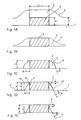
- FIG. 1 schematically illustrates the structure which must be produced before the etching operation intended for the production of the spacers.
- a layer of a first material is deposited, over a thickness e.
- An operation, known per se, is then carried out of photolithography and anisotropic etching leading to the production, from the initially deposited layer, of patterns 2 having a rectangular cross section.
- a layer 3 of a second material over a thickness f is then deposited over the entire wafer.
- Layer 3 can be deposited by spraying or by a chemical vapor deposition process.
- the upper surface 4 of the layer 3 is horizontal in the zones located on the underlying zones which are themselves horizontal and is clearly inclined in the transient zones corresponding to a step change.
- FIG. 1C represents this etching stage during which the spacers 7 are produced.
- the inhomogeneities of deposition and etching can be compensated for by continuing the etching operation up to the stage shown in FIG. 1D. If etching is continued, a thinning of the spacer 7 is obtained, its height h is significantly reduced and its width l is also reduced, as shown in FIG. 1E. By continuing the etching even more, it is possible to obtain the total elimination of the spacer 7 (not shown). It should be noted that this further etching is accompanied by the consumption of the substrate 1.
- the difficulty in producing the spacers lies in the fact that it is necessary to stop the etching operation at a precise instant in order to obtain a spacer of the desired shape (as shown in FIG. 1D).
- many other factors are likely to create disparities in the constitution of the spacers 7. Indeed, if the initial thickness f of the layer 3 is slightly too large or too small, the spacer 7 which will result therefrom the engraving operation will not be in conformity. If, moreover, the material constituting the layer 3 has characteristics slightly different from those considered to be normal, it may cause a higher or lower etching speed, also leading to the production of non-conforming spacers 7.
- the actual etching process can also be subject to unwanted variations resulting from certain misadjustments of machines or equipment.
- the invention as will be seen in the detailed description which follows, makes it possible to meet these wishes.
- FIGS. 2, 3 and 4 Reference will now be made essentially to FIGS. 2, 3 and 4 to describe in more detail the measurement method according to the present invention.
- FIGS. 1A to 1E represent either microstructures of integrated circuits with which it is desired to associate spacers 7 or else parallel strips forming a network to which it is also envisaged to associate spacers 7 intended for dimensional control.
- spacers are then produced on the lateral edges 6 of the parallel strips 2.
- the steps described in relation to FIG. 1 are carried out.
- the network 2 is illuminated with a monochromatic light beam.
- the light diffracted by the grating produces a diffraction pattern composed of a main light spot 15 corresponding to the specular reflection and of a multitude of adjacent aligned diffraction spots whose envelope has a lobe main L0 including the main spot 15 and secondary lobes among which the first lobe L1 is adjacent to the main lobe L0.
- the present invention measures the light intensity of spots constituting the first lobe L1.
- a group of spots of the lobe L1 will preferably be selected, the light intensity of which varies notably with the degree of etching of the spacer.
- the present invention is based on the observation made by the applicant that this light intensity measurement IL1 can be deduced from one or more spots of the first lobe L1, the width l, the angle ⁇ and the difference in height. d, by comparison with calibration curves.
- the light intensity IL1 of the first lobe L1 is in linear relationship, both with the width l of the spacer 7, the angle ⁇ of the spacer 7 and the difference in height d when the latter is negative, that is to say when the height h of the spacer 7 is less than the thickness e of the parallel strips 2.
- FIG. 3 represents the linear relationship between the measurement of light intensity IL1 and the width l of the spacer.
- the light intensity of lobe L1 increases when the width l of the spacer 7 decreases.
- We can therefore easily, by a set of preliminary experimental measurements or by a simulation, determine the linear function connecting l and IL1 by a function of the type: l k1 ⁇ IL1 + k2 in which k1 and k2 are two constants.
- FIG. 4 represents the linear relationship between the parameter IL1 and ⁇ .
- ⁇ k3 ⁇ IL1 + k4, in which k3 and k4 are two constants.
- FIG. 5 represents the evolution of the algebraic value d during the etching operation as a function of the light intensity of a determined group of spots belonging to the first lobe 1.
- the very beginning of the etching operation corresponds to FIG. 1A.
- the mark B in Figure 5 corresponds to the level of engraving in Figure 1B, and so on for the marks C, D and E.
- the marks C, D and E correspond respectively to level of etching shown in Figures 1C, 1D and 1E.
- the light intensity IL1 has increased to that the etching reaches the state shown in Figure 1C, that is to say when the horizontal areas of the layer 3 are completely removed.
- the states represented in FIGS. 1D and 1E it can be seen that the light intensity IL1 has evolved linearly as a function of the algebraic value d.
- the group of spots of the first lobe L1 should be chosen such that the intensity IL1 passes through an optimum for the level of etching corresponding to point C.
- the invention can be easily implemented using an appropriate device (not shown).
- This device essentially comprises a monochromatic light source, generally a laser source, which strikes at a determined angle of incidence, the network of parallel bands.
- the apparatus also comprises a detector which is situated at the level of the diffraction spots and which may consist, for example, of a strip of CCD sensors.
- the apparatus then comprises, in a manner known per se, a set of electronic devices making it possible to locate the different light spots, to spot the spot 15 corresponding to the specular reflection, to count the different spots and to spot the first lobe L1 and, in this lobe L1, the brightest spot 16.
- the device can then carry out the intensity measurements IL1 corresponding to the process described above and carry out very simple calculations to directly edit the values of the parameters l, ⁇ and d.
Abstract
Description
La présente invention concerne un procédé pour mesurer les dimensions caractéristiques d'un espaceur ou d'une structure analogue utilisé en particulier lors de la fabrication de certains circuits intégrés.The present invention relates to a method for measuring the characteristic dimensions of a spacer or a similar structure used in particular during the manufacture of certain integrated circuits.
La présente invention s'applique notamment au domaine des circuits intégrés où elle est utile pour certaines opérations de contrôle de qualité en cours de fabrication.The present invention applies in particular to the field of integrated circuits where it is useful for certain quality control operations during manufacture.
Dans la réalisation de certains circuits intégrés, on est amené à constituer des structures particulières qui sont appelées des espaceurs.In the production of certain integrated circuits, it is necessary to constitute particular structures which are called spacers.
Un espaceur est constitué d'un résidu d'un certain matériau, localisé exclusivement contre les bords latéraux verticaux des structures présentes au moment de l'étape de réalisation de l'espaceur.A spacer consists of a residue of a certain material, located exclusively against the vertical lateral edges of the structures present at the time of the step of making the spacer.
Pour réaliser des espaceurs, on dépose une couche d'épaisseur uniforme d'un certain matériau sur la plaquette en cours de traitement, puis on effectue une gravure anisotrope de cette couche. L'opération de gravure de cette couche est arrêtée dès que les zones de cette couche situées sur des parties horizontales ou inclinées des structures sous-jacentes sont totalement enlevées. Dans ces conditions, les parties de cette couche situées, très localement, contre les bords latéraux verticaux des structures sous-jacentes ne sont que partiellement gravées et laissent donc subsister localement un bourrelet de très faible largeur qui constitue l'espaceur. Cette technique présente essentiellement l'avantage de pouvoir réaliser certaines microstructures de façon autoalignée, sans opération de masquage et de photolithographie. Les espaceurs ont trouvé en microélectronique plusieurs applications, en particulier lors de la réalisation de drains faiblement dopés, correspondant à la technique appelée LDD (Lightly Doped Drain), lors du dépôt de siliciure sur les drains, les sources et les grilles sans court-circuit entre ces différentes parties, ou afin d'adoucir des marches pour permettre un meilleur passage des couches déposées par dessus.To make spacers, a layer of uniform thickness of a certain material is deposited on the wafer during treatment, then anisotropic etching of this layer is carried out. The etching operation of this layer is stopped as soon as the areas of this layer located on horizontal or inclined parts of the underlying structures are completely removed. Under these conditions, the parts of this layer located, very locally, against the vertical lateral edges of the underlying structures are only partially etched and therefore leave locally a bead of very small width which constitutes the spacer. This technique essentially has the advantage of being able to produce certain microstructures in a self-aligned manner, without masking and photolithography. Spacers have found several applications in microelectronics, in particular when producing lightly doped drains, corresponding to the technique called LDD (Lightly Doped Drain), when depositing silicide on drains, sources and grids without short circuits. between these different parts, or to soften steps to allow better passage of the layers deposited on top.
Dans tous les cas où l'on a ainsi recours à la constitution d'espaceurs, il est nécessaire de contrôler, lors de la fabrication, les formes géométriques des espaceurs et de pouvoir effectuer certaines mesures dimensionnelles. Ces contrôles sont d'autant plus nécessaires que les opérations technologiques conduisant à la constitution des espaceurs sont difficiles à maîtriser et sont sujettes à des dérives, en particulier du fait que l'opération de gravure doit être interrompue brusquement. Si l'on interrompt la gravure trop tôt ou trop tard, si la vitesse de gravure est plus grande ou plus faible que celle prévue, l'espaceur qui en résulte ne présente plus la même forme ni les mêmes dimensions.In all cases where recourse is made to the creation of spacers, it is necessary to check, during manufacture, the geometric shapes of the spacers and to be able to carry out certain dimensional measurements. These controls are all the more necessary as the technological operations leading to the constitution of the spacers are difficult to control and are subject to drifts, in particular because the etching operation must be abruptly interrupted. If the etching is interrupted too early or too late, if the etching speed is higher or lower than that expected, the resulting spacer no longer has the same shape or the same dimensions.
Un procédé connu pour contrôler la forme et les dimensions des espaceurs consiste à casser une plaquette transversalement aux espaceurs et à examiner la coupe transversale au travers d'un microscope électronique. Cette méthode est chère, longue et délicate. En plus, elle est destructive. On ne connaît pas à ce jour de procédé de contrôle des espaceurs fiable, non destructif et immédiat.A known method for controlling the shape and dimensions of the spacers is to break a wafer transversely to the spacers and examine the cross section through an electron microscope. This method is expensive, long and delicate. In addition, it is destructive. To date, no reliable, non-destructive and immediate control method for spacers is known.
Ainsi, un objet de la présente invention est de prévoir un procédé permettant la mesure des dimensions caractéristiques des espaceurs.It is therefore an object of the present invention to provide a method for measuring the characteristic dimensions of the spacers.
Pour atteindre ces objets, la présente invention prévoit un procédé de mesure des dimensions d'un espaceur consistant à:
- former sur un substrat un réseau de bandes parallèles, chaque bande ayant une section transversale rectangulaire;
- réaliser des espaceurs sur les bords latéraux des bandes parallèles, ces espaceurs présentant, selon une section transversale, une largeur ℓ correspondant à la distance séparant le bord de la bande et le bord extérieur de l'espaceur au niveau de leur contact avec le substrat, et un angle ϑ que forme, avec le plan du substrat, la tangente au bord extérieur de l'espaceur au niveau du substrat;
- au cours de l'étape de réalisation des espaceurs ou à la suite de celle-ci, éclairer le réseau par un faisceau lumineux monochromatique dont la lumière diffractée produit une figure de diffraction composée d'une tache lumineuse principale correspondant à la réflexion spéculaire et d'une multitude de taches adjacentes alignées de diffraction dont l'enveloppe présente un lobe principal incluant la tache principale et des lobes secondaires parmi lesquels le premier lobe est adjacent au lobe principal;
- mesurer la somme des intensités lumineuses d'un nombre prédéterminé de taches appartenant au premier lobe; et
- en déduire la largeur ℓ et l'angle ϑ de l'espaceur par les formules suivantes:


- forming on a substrate an array of parallel strips, each strip having a rectangular cross section;
- making spacers on the lateral edges of the parallel strips, these spacers having, along a cross section, a width ℓ corresponding to the distance separating the edge of the strip and the outer edge of the spacer at their contact with the substrate, and an angle ϑ which forms, with the plane of the substrate, the tangent to the outer edge of the spacer at the substrate;
- during the step of making the spacers or as a result thereof, illuminating the network with a monochromatic light beam whose diffracted light produces a diffraction pattern composed of a main light spot corresponding to the specular reflection and d 'a multitude of adjacent aligned diffraction spots, the envelope of which has a main lobe including the main spot and secondary lobes among which the first lobe is adjacent to the main lobe;
- measuring the sum of the light intensities of a predetermined number of spots belonging to the first lobe; and
- deduce the width ℓ and the angle ϑ of the spacer by the following formulas:
L'espaceur présentant une hauteur h correspondant, selon une section transversale, à la distance séparant le bord supérieur de l'espaceur en contact avec le bord latéral de la bande parallèle et la surface du substrat, et la valeur algébrique d correspondant à la différence entre la hauteur h et l'épaisseur e de la bande parallèle, on déduit la valeur algébrique d par la formule suivante:![]()
![]()
Ces objets, caractéristiques et avantages ainsi que d'autres de la présente invention seront exposés plus en détail dans la description suivante d'un mode de réalisation particulier faite en relation avec les figures jointes parmi lesquelles:
- la figure 1A représente schématiquement, en coupe transversale, les couches existantes avant la gravure destinée à la réalisation des espaceurs;
- la figure 1B représente schématiquement, en coupe transversale, la même structure que la figure 1A mais à un stade intermédiaire de la gravure destinée à la réalisation des espaceurs;
- la figure 1C représente schématiquement, en coupe transversale, la même structure à un stade de gravure plus avancé;
- la figure 1D représente schématiquement, en coupe transversale, la même structure à un stade de gravure encoure plus avancé, correspondant à l'élaboration correcte des espaceurs;
- la figure 1E représente schématiquement, en coupe transversale, la même structure résultant d'une surgravure des espaceurs;
- la figure 2 représente le diagramme de diffraction obtenu lors de la mise en oeuvre de l'invention;
- la figure 3 représente la courbe établissant la relation linéaire entre la largeur de l'espaceur et la mesure d'intensité lumineuse selon l'invention;
- la figure 4 représente la courbe établissant la relation linéaire entre l'angle ϑ et la mesure d'intensité lumineuse selon l'invention; et
- la figure 5 représente la courbe établissant la relation entre le décrochement d et la mesure d'intensité lumineuse selon l'invention.
- FIG. 1A schematically represents, in cross section, the layers existing before the etching intended for the production of the spacers;
- FIG. 1B schematically represents, in cross section, the same structure as FIG. 1A but at an intermediate stage of the etching intended for the production of the spacers;
- FIG. 1C schematically represents, in cross section, the same structure at a more advanced etching stage;
- FIG. 1D schematically represents, in cross section, the same structure at a more advanced stage of etching, corresponding to the correct development of the spacers;
- FIG. 1E schematically represents, in cross section, the same structure resulting from an over-etching of the spacers;
- FIG. 2 represents the diffraction diagram obtained during the implementation of the invention;
- FIG. 3 represents the curve establishing the linear relationship between the width of the spacer and the measurement of light intensity according to the invention;
- FIG. 4 represents the curve establishing the linear relationship between the angle ϑ and the measurement of light intensity according to the invention; and
- FIG. 5 represents the curve establishing the relationship between the offset d and the measurement of light intensity according to the invention.
La figure 1 illustre de façon schématique la structure que l'on doit réaliser avant l'opération de gravure destinée à la réalisation des espaceurs. Sur un substrat 1, constitué généralement d'une plaquette en matériau semiconducteur, on dépose une couche d'un premier matériau, sur une épaisseur e. On effectue ensuite une opération, connue en soi, de photolithographie et de gravure anisotrope conduisant à la réalisation, à partir de la couche déposée initialement, de motifs 2 présentant une section transversale rectangulaire. On dépose ensuite sur toute la plaquette une couche 3 d'un second matériau sur une épaisseur f. La couche 3 peut être déposée par pulvérisation ou par un procédé de dépôt chimique en phase vapeur. La surface supérieure 4 de la couche 3 est horizontale dans les zones situées sur des zones sous-jacentes elles-mêmes horizontales et est nettement inclinée dans les zones transitoires correspondant à un passage de marche.FIG. 1 schematically illustrates the structure which must be produced before the etching operation intended for the production of the spacers. On a
On effectue ensuite une opération de gravure anisotrope par un procédé quelconque connu de l'art antérieur. Dans une première phase de cette gravure, comme cela est représenté en figure 1B, la surface supérieure 4 de la couche 3 conserve sensiblement le même profil. On dit que, dans cette phase de gravure, le profil est transféré. On se retrouve alors avec un très net amincissement de l'épaisseur de la couche 3 dans les zones horizontales et une présence relativement importante de matériau de la couche 3 au niveau 5 du passage de marche, c'est-à-dire dans les zones où la surface supérieure 4 de la couche 3 est fortement inclinée.An anisotropic etching operation is then carried out by any method known from the prior art. In a first phase of this etching, as shown in FIG. 1B, the
En poursuivant encore la gravure, on obtient l'enlèvement complet de la couche 3 dans toutes les zones horizontales, et il ne reste plus alors que des bandes étroites, indépendantes, constituées du matériau de la couche 3, longeant les bords latéraux verticaux 6 des motifs 2. Ces bandes étroites 7 sont appelées alors des espaceurs. La figure 1C représente ce stade de gravure au cours duquel on a réalisé les espaceurs 7.By continuing the etching, the complete removal of the
On peut compenser les inhomogénéités de dépôt et de gravure en poursuivant l'opération de gravure jusqu'au stade représenté en figure 1D. Si l'on poursuit encore la gravure, on obtient un amincissement de l'espaceur 7, sa hauteur h se trouve nettement réduite et sa largeur l est réduite également, comme cela est représenté en figure 1E. En poursuivant encore davantage la gravure, on peut obtenir l'élimination totale de l'espaceur 7 (non représenté). Il faut noter que cette poursuite de gravure s'accompagne de la consommation du substrat 1.The inhomogeneities of deposition and etching can be compensated for by continuing the etching operation up to the stage shown in FIG. 1D. If etching is continued, a thinning of the
Lors de la fabrication de circuits intégrés, la difficulté de réalisation des espaceurs réside dans le fait qu'il faut arrêter à un instant précis l'opération de gravure pour obtenir un espaceur de forme voulue (tel que représenté en figure 1D). En plus, de nombreux autres facteurs sont susceptibles de créer des disparités dans la constitution des espaceurs 7. En effet, si l'épaisseur initiale f de la couche 3 est légèrement trop grande ou trop faible, l'espaceur 7 qui en résultera après l'opération de gravure ne sera pas conforme. Si, par ailleurs, le matériau constituant la couche 3 présente des caractéristiques légèrement différentes de celles considérées comme normales, il peut entraîner une vitesse de gravure plus grande ou plus faible, conduisant également à la réalisation d'espaceurs 7 non conformes. Le procédé même de gravure peut également être soumis à des variations non souhaitées résultant de certains déréglages des machines ou des équipements. On voit par conséquent l'intérêt d'un contrôle dimensionnel précis et fiable des espaceurs. On comprend aussi qu'il est souhaitable que ce contrôle dimensionnel des espaceurs 7 s'effectue très rapidement, pour éviter de fabriquer un trop grand nombre de pièces mauvaises pendant le temps séparant la fabrication et les résultats du contrôle. On voit également qu'il serait très avantageux de pouvoir contrôler les dimensions de l'espaceur 7 pendant l'opération de gravure elle-même, c'est-à-dire de pouvoir opérer un contrôle in situ. L'invention, comme on va le voir dans la description détaillée qui va suivre, permet de répondre à ces souhaits.During the manufacture of integrated circuits, the difficulty in producing the spacers lies in the fact that it is necessary to stop the etching operation at a precise instant in order to obtain a spacer of the desired shape (as shown in FIG. 1D). In addition, many other factors are likely to create disparities in the constitution of the
Avant de décrire plus en détail le procédé selon l'invention, on va décrire précisément les différentes grandeurs physiques représentatives de la forme de la section transversale de l'espaceur 7, en se référant à la figure 1D. La section transversale de l'espaceur 7 présente une forme générale s'approchant d'un triangle dont le côté opposé à l'angle droit est légèrement bombé. Cette caractéristique n'est pas essentielle pour comprendre l'objet de la présente invention. D'ailleurs, dans certains procédés de réalisation d'espaceurs ceux-ci peuvent présenter des formes légèrement différentes. Cependant, dans tous les espaceurs que l'on réalise actuellement, on retrouve cette forme générale approximative de triangle et l'on peut toujours définir les trois grandeurs caractéristiques h, ℓ et ϑ de la manière suivante:
- la hauteur h de l'espaceur 7 correspond à la distance séparant le bord supérieur 8 de l'espaceur, en contact avec le bord latéral vertical 6
du motif 2, et la surface supérieure plane 9 du substrat 1; - la largeur ℓ est égale à la distance séparant le bord latéral 6 du
motif 2, au niveau de son contact avec le substrat 1, et le bord extérieur 10 de l'espaceur 7, au niveau de son contact avec le substrat 1; et - l'angle ϑ est l'angle que forme la tangente 11 au bord extérieur 10 de l'espaceur, au niveau de son contact avec le substrat 1.
- the height h of the
spacer 7 corresponds to the distance separating theupper edge 8 of the spacer, in contact with the verticallateral edge 6 of thepattern 2, and the planar upper surface 9 of thesubstrate 1; - the width ℓ is equal to the distance separating the
lateral edge 6 of thepattern 2, at its contact with thesubstrate 1, and theouter edge 10 of thespacer 7, at its contact with thesubstrate 1; and - the angle ϑ is the angle formed by the tangent 11 at the
outer edge 10 of the spacer, at its contact with thesubstrate 1.
On définit en plus la différence de hauteur d selon la formule algébrique suivante:![]()
![]()
On se référera maintenant essentiellement aux figures 2,3 et 4 pour décrire plus en détail le procédé de mesure selon la présente invention.Reference will now be made essentially to FIGS. 2, 3 and 4 to describe in more detail the measurement method according to the present invention.
Lorsque l'on effectue l'opération de réalisation d'espaceurs sur des plaquettes destinées à constituer par la suite des circuits intégrés, on dispose toujours, sur certaines régions de ces plaquettes, d'espaces dépourvus de circuits intégrés, servant essentiellement à diverses opérations de test et de contrôle.When performing the operation of making spacers on wafers intended to subsequently constitute integrated circuits, there are always, in certain regions of these wafers, spaces devoid of integrated circuits, essentially used for various operations test and control.
Dans une de ces zones libres, il est toujours possible de ménager certaines structures particulières qui sont réalisées simultanément avec des opérations correspondantes destinées à la fabrication des circuits intégrés. Dans au moins une de ces zones libres, on forme un réseau de bandes parallèles lors des mêmes étapes technologiques que celles destinées à constituter dans les circuits les microstructures aux bords 6 desquelles on envisage d'associer des espaceurs. On réalise donc un réseau de bandes parallèles 2 en un premier matériau correspondant à celui de ces microstructures. Chaque bande parallèle présente une section transversale approximativement rectangulaire. On peut considérer que les figures 1A à 1E représentent ou bien des microstructures de circuits intégrés auxquels on souhaite associer des espaceurs 7 ou bien des bandes parallèles formant un réseau auquel on envisage également d'associer des espaceurs 7 destinés au contrôle dimensionnel. Selon la présente invention, on réalise ensuite des espaceurs sur les bords latéraux 6 des bandes parallèles 2. Pour cela, on procède aux étapes décrites en relation avec la figure 1. Au cours de l'opération de gravure anisotrope, ou après que cette opération de gravure soit terminée, on éclaire le réseau 2 par un faisceau lumineux monochromatique. Comme cela est représenté en figure 2, la lumière diffractée par le réseau produit une figure de diffraction composée d'une tache lumineuse principale 15 correspondant à la réflexion spéculaire et d'une multitude de taches adjacentes alignées de diffraction dont l'enveloppe présente un lobe principal L0 incluant la tache principale 15 et des lobes secondaires parmi lesquels le premier lobe L1 est adjacent au lobe principal L0. Selon la présente invention, on effectue la mesure de l'intensité lumineuse de taches constituant le premier lobe L1. On peut, soit mesurer l'intensité lumineuse de la tache la plus brillante 16 du premier lobe L1, soit faire la somme des mesures des intensités lumineuses d'un nombre prédéterminé de taches appartenant au premier lobe L1, les taches ainsi prises en compte ne correspondant pas obligatoirement aux taches les plus lumineuses de ce premier lobe L1. On peut également prendre en considération toutes les taches incluses dans le premier lobe L1, c'est-à-dire mesurer l'intensité lumineuse globale du premier lobe L1. En fait, on sélectionnera de préférence un groupe de taches du lobe L1 dont l'intensité lumineuse varie notablement avec le degré de gravure de l'espaceur.In one of these free zones, it is always possible to provide certain specific structures which are produced simultaneously with corresponding operations intended for the manufacture of integrated circuits. In at least one of these free zones, a network of parallel strips is formed during the same technological steps as those intended to constitute in the circuits the microstructures at the
La présente invention se base sur l'observation faite par la demanderesse selon laquelle on peut déduire cette mesure d'intensité lumineuse IL1 d'une ou plusieurs taches du premier lobe L1, la largeur ℓ, l'angle ϑ ainsi que la différence de hauteur d, par comparaison avec des courbes d'étalonnage.The present invention is based on the observation made by the applicant that this light intensity measurement IL1 can be deduced from one or more spots of the first lobe L1, the width ℓ, the angle ϑ and the difference in height. d, by comparison with calibration curves.
En effet, il a été constaté que l'intensité lumineuse IL1 du premier lobe L1 est en relation linéaire, à la fois avec la largeur ℓ de l'espaceur 7, l'angle ϑ de l'espaceur 7 et la différence de hauteur d lorsque celle-ci est négative, c'est-à-dire lorsque la hauteur h de l'espaceur 7 est inférieure à l'épaisseur e des bandes parallèles 2.Indeed, it was found that the light intensity IL1 of the first lobe L1 is in linear relationship, both with the width ℓ of the
La figure 3 représente la relation linéaire entre la mesure d'intensité lumineuse IL1 et la largeur ℓ de l'espaceur. On voit que l'intensité lumineuse du lobe L1 croît lorsque la largeur ℓ de l'espaceur 7 décroît. On peut donc aisément, par un ensemble de mesures expérimentales préalables ou par une simulation, déterminer la fonction linéaire reliant ℓ et IL1 par une fonction du type:![]()
![]()
La figure 4 représente la relation linéaire entre le paramètre IL1 et ϑ. On peut établir pareillement la formule suivante:![]()
![]()
La figure 5 représente l'évolution de la valeur algébrique d au cours de l'opération de gravure en fonction de l'intensité lumineuse d'un groupe déterminé de taches appartenant au premier lobe 1. Le tout début de l'opération de gravure, correspondant au repère A, correspond à la figure 1A. Le repère B de la figure 5 correspond au niveau de gravure de la figure 1B, et ainsi de suite pour les repères C, D et E. De même, dans les figures 3 et 4, les repères C, D et E correspondent respectivement au niveau de gravure représenté dans les figures 1C, 1D et 1E.FIG. 5 represents the evolution of the algebraic value d during the etching operation as a function of the light intensity of a determined group of spots belonging to the
En se reportant à nouveau à la figure 5, on remarque que, pour le groupe de taches choisi dans cet exemple particulier, au début de la gravure, correspondant au repère A, B et C, l'intensité lumineuse IL1 a cru jusqu'à ce que la gravure parvienne à l'état représenté en figure 1C, c'est-à-dire au moment où les zones horizontales de la couche 3 sont totalement enlevées. Lorsque l'on a poursuivi la gravure, en passant successivement dans les états représentés dans les figures 1D et 1E, on voit que l'intensité lumineuse IL1 a évolué linéairement en fonction de la valeur algébrique d. Par conséquent, dans la plage C, D et E, on a pu déterminer pareillement une fonction linéaire entre l'intensité lumineuse IL1 et la grandeur physique d, correspondant à la formule suivante:![]()
![]()
Pour déterminer les constantes k1 et k6, on procédera à un étalonnage préalable sur des espaceurs de forme et de dimensions connues, déterminées, par exemple, par microscopie électronique.To determine the constants k1 and k6, a prior calibration will be carried out on spacers of known shape and dimensions, determined, for example, by electron microscopy.
On notera par ailleurs que, au moment où les zones horizontales de la couches 3 sont complètement gravées, c'est-à-dire quand on se trouve dans la configuration de la figure 1C, l'intensité lumineuse IL1 passe par un maximum, facilement décelable par des moyens de mesures classiques. On peut donc aisément déterminer cet instant précis correspondant au point C et effectuer de la sorte un système de détection de fin d'attaque.It will also be noted that, when the horizontal zones of the
On notera que, pour obtenir une détection de fin d'attaque satisfaisante, il convient de choisir le groupe de taches du premier lobe L1 tel que l'intensité IL1 passe par un optimum pour le niveau de gravure correspondant au point C.It will be noted that, to obtain a satisfactory end of attack detection, the group of spots of the first lobe L1 should be chosen such that the intensity IL1 passes through an optimum for the level of etching corresponding to point C.
L'invention peut être aisément mise en oeuvre à l'aide d'un appareil approprié (non représenté).The invention can be easily implemented using an appropriate device (not shown).
Cet appareil comporte essentiellement une source de lumière monochromatique, en général une source laser, qui vient frapper selon un angle d'incidence déterminé, le réseau de bandes parallèles. L'appareil comporte également un détecteur qui est situé au niveau des taches de diffraction et qui peut être constitué, par exemple d'une barrette de capteurs CCD. L'appareil comporte ensuite, de façon connue en soi, un ensemble de dispositifs électroniques permettant de repérer les différentes taches lumineuses, de repérer la tache 15 correspondant à la réflexion spéculaire, de compter les différentes taches et de repérer le premier lobe L1 et, dans ce lobe L1, la tache 16 la plus lumineuse. L'appareil peut alors effectuer les mesures d'intensité IL1 correspondant au procédé précédemment décrit et effectuer les calculs fort simples pour éditer directement les valeurs des paramètres ℓ, ϑ et d.This device essentially comprises a monochromatic light source, generally a laser source, which strikes at a determined angle of incidence, the network of parallel bands. The apparatus also comprises a detector which is situated at the level of the diffraction spots and which may consist, for example, of a strip of CCD sensors. The apparatus then comprises, in a manner known per se, a set of electronic devices making it possible to locate the different light spots, to spot the
Claims (2)
caractérisé en ce qu'il comprend les étapes suivantes:
characterized in that it comprises the following stages:
Priority Applications (1)
| Application Number | Priority Date | Filing Date | Title |
|---|---|---|---|
| AT90420552T ATE104428T1 (en) | 1989-12-21 | 1990-12-18 | PROCEDURE FOR MEASURING THE DIMENSIONS OF A SPACER. |
Applications Claiming Priority (2)
| Application Number | Priority Date | Filing Date | Title |
|---|---|---|---|
| FR8917387 | 1989-12-21 | ||
| FR8917387A FR2656465B1 (en) | 1989-12-21 | 1989-12-21 | METHOD FOR MEASURING THE DIMENSIONS OF A SPACER. |
Publications (3)
| Publication Number | Publication Date |
|---|---|
| EP0446549A2 true EP0446549A2 (en) | 1991-09-18 |
| EP0446549A3 EP0446549A3 (en) | 1991-09-25 |
| EP0446549B1 EP0446549B1 (en) | 1994-04-13 |
Family
ID=9389103
Family Applications (1)
| Application Number | Title | Priority Date | Filing Date |
|---|---|---|---|
| EP90420552A Expired - Lifetime EP0446549B1 (en) | 1989-12-21 | 1990-12-18 | Procedure to measure the dimensions of a spacer |
Country Status (6)
| Country | Link |
|---|---|
| US (1) | US5103104A (en) |
| EP (1) | EP0446549B1 (en) |
| JP (1) | JP2857495B2 (en) |
| AT (1) | ATE104428T1 (en) |
| DE (1) | DE69008156T2 (en) |
| FR (1) | FR2656465B1 (en) |
Families Citing this family (9)
| Publication number | Priority date | Publication date | Assignee | Title |
|---|---|---|---|---|
| US5805290A (en) * | 1996-05-02 | 1998-09-08 | International Business Machines Corporation | Method of optical metrology of unresolved pattern arrays |
| US5965309A (en) * | 1997-08-28 | 1999-10-12 | International Business Machines Corporation | Focus or exposure dose parameter control system using tone reversing patterns |
| US5976740A (en) * | 1997-08-28 | 1999-11-02 | International Business Machines Corporation | Process for controlling exposure dose or focus parameters using tone reversing pattern |
| US5953128A (en) * | 1997-08-28 | 1999-09-14 | International Business Machines Corporation | Optically measurable serpentine edge tone reversed targets |
| US5914784A (en) * | 1997-09-30 | 1999-06-22 | International Business Machines Corporation | Measurement method for linewidth metrology |
| US6137578A (en) * | 1998-07-28 | 2000-10-24 | International Business Machines Corporation | Segmented bar-in-bar target |
| US6128089A (en) * | 1998-07-28 | 2000-10-03 | International Business Machines Corporation | Combined segmented and nonsegmented bar-in-bar targets |
| GB2340980A (en) * | 1998-08-21 | 2000-03-01 | Ezio Panzeri | A coded token |
| US7400417B2 (en) * | 2005-05-23 | 2008-07-15 | Federal Mogul World Wide, Inc. | Diffraction method for measuring thickness of a workpart |
Citations (3)
| Publication number | Priority date | Publication date | Assignee | Title |
|---|---|---|---|---|
| JPS56120904A (en) * | 1980-02-29 | 1981-09-22 | Chugoku Toryo Kk | Measuring method for rate of removal of coating film |
| US4767495A (en) * | 1986-12-10 | 1988-08-30 | Dainippon Screen Mfg. Co., Ltd. | Method for detecting time for termination of surface layer removal processing |
| EP0320425A2 (en) * | 1987-12-09 | 1989-06-14 | International Business Machines Corporation | Plasma amplified photoelectron process endpoint detection apparatus |
Family Cites Families (5)
| Publication number | Priority date | Publication date | Assignee | Title |
|---|---|---|---|---|
| JPS60196605A (en) * | 1984-03-19 | 1985-10-05 | Nippon Kogaku Kk <Nikon> | Scattering-light detecting optical device |
| US4842411A (en) * | 1986-02-06 | 1989-06-27 | Vectron, Inc. | Method of automatically measuring the shape of a continuous surface |
| JPH07122574B2 (en) * | 1986-07-25 | 1995-12-25 | 株式会社日立製作所 | Cross-sectional shape measurement method |
| JP2542653B2 (en) * | 1987-12-10 | 1996-10-09 | ファナック株式会社 | Non-contact copying method |
| US5024949A (en) * | 1989-02-17 | 1991-06-18 | Biotrol, Inc. | Aerobic bacterial remediation of aliphatic chlorinated hydrocarbon contamination |
-
1989
- 1989-12-21 FR FR8917387A patent/FR2656465B1/en not_active Expired - Lifetime
-
1990
- 1990-12-18 AT AT90420552T patent/ATE104428T1/en not_active IP Right Cessation
- 1990-12-18 DE DE69008156T patent/DE69008156T2/en not_active Expired - Fee Related
- 1990-12-18 EP EP90420552A patent/EP0446549B1/en not_active Expired - Lifetime
- 1990-12-20 US US07/631,733 patent/US5103104A/en not_active Expired - Lifetime
- 1990-12-20 JP JP2404108A patent/JP2857495B2/en not_active Expired - Lifetime
Patent Citations (3)
| Publication number | Priority date | Publication date | Assignee | Title |
|---|---|---|---|---|
| JPS56120904A (en) * | 1980-02-29 | 1981-09-22 | Chugoku Toryo Kk | Measuring method for rate of removal of coating film |
| US4767495A (en) * | 1986-12-10 | 1988-08-30 | Dainippon Screen Mfg. Co., Ltd. | Method for detecting time for termination of surface layer removal processing |
| EP0320425A2 (en) * | 1987-12-09 | 1989-06-14 | International Business Machines Corporation | Plasma amplified photoelectron process endpoint detection apparatus |
Non-Patent Citations (2)
| Title |
|---|
| IBM TECHNICAL DISCLOSURE BULLETIN, vol. 21, no. 11, avril 1979, pages 4477-4480, Armonk, NY, US; R.B. ANANTAKRISHNAN: "System to satisfy the residual first quarz process requirement" * |
| PATENT ABSTRACTS OF JAPAN, vol. 5, no. 201 (P-94)[873], 19 décembre 1981; & JP-A-56 120 904 (CHIYUUGOKU TORIYOU K.K.) 22-09-1981 * |
Also Published As
| Publication number | Publication date |
|---|---|
| JPH06180210A (en) | 1994-06-28 |
| FR2656465A1 (en) | 1991-06-28 |
| DE69008156T2 (en) | 1994-12-01 |
| EP0446549A3 (en) | 1991-09-25 |
| DE69008156D1 (en) | 1994-05-19 |
| US5103104A (en) | 1992-04-07 |
| EP0446549B1 (en) | 1994-04-13 |
| JP2857495B2 (en) | 1999-02-17 |
| FR2656465B1 (en) | 1992-05-07 |
| ATE104428T1 (en) | 1994-04-15 |
Similar Documents
| Publication | Publication Date | Title |
|---|---|---|
| EP0446549B1 (en) | Procedure to measure the dimensions of a spacer | |
| EP0487380A1 (en) | Process for etching layers at a given depth in integrated circuits | |
| EP2277084A1 (en) | Method for the real-time monitoring of integrated circuit manufacture through localized monitoring structures in opc model space | |
| IL123727A (en) | Method and apparatus for measurement of patterned structures | |
| EP0766060A1 (en) | Micromechanical part having at least one tip consisting of diamond, and manufacturing method for such parts. | |
| FR2534022A1 (en) | METHOD FOR PRODUCING STRESS-SENSITIVE ELEMENT, DEVICE FOR CONVERTING MECHANICAL MOVEMENT IN ELECTRIC SIGNALS, AND TRANSDUCER | |
| EP0468897B1 (en) | Process for the determination of the complete removal of a thin film on a non-planar substrate | |
| FR2951543A1 (en) | METHOD FOR ANALYZING THE QUALITY OF A GLAZING | |
| EP0294873A1 (en) | Test apparatus for performing a realization process of semiconductor structures | |
| EP1439580B1 (en) | Fabrication of fine and narrow-spaced trenches | |
| US7839509B2 (en) | Method of measuring deep trenches with model-based optical spectroscopy | |
| CA2457899C (en) | Colour image sensor on transparent substrate and method for making same | |
| EP1922539B1 (en) | Method and device to quantify active charge carrier profiles in ultra-shallow semiconductor structures | |
| FR2974240A1 (en) | REAR-SIDED LIGHT-SENSING SENSOR BY JUNCTION | |
| FR2829292A1 (en) | METHOD FOR MANUFACTURING COLOR IMAGE SENSOR WITH PLOT ON PLOT WELDED SUPPORT SUBSTRATE | |
| FR2972293A1 (en) | METHOD FOR MANUFACTURING AN INTEGRATED CIRCUIT ON THE FORMATION OF LINES AND SLICES | |
| EP0378033A1 (en) | Process for setting up a photolithographic exposure machine | |
| EP0262055B1 (en) | Flow-measuring process | |
| EP0274966B1 (en) | Process for the quantitative determination of the shape of relief patterns having very small dimensions | |
| FR2754905A1 (en) | METHOD FOR MAKING A MAGNETORESISTIVE MAGNETIC SENSOR AND SENSOR OBTAINED BY THIS METHOD | |
| JP3003642B2 (en) | Standard sample for calibration of foreign object detection sensitivity and method for producing the same | |
| TWI276832B (en) | Method of sample preparation for scanning capacitance microscope and measuring method thereby | |
| EP0493269B1 (en) | Method for measuring the viscosity of a material | |
| FR2651068A1 (en) | PROCESS FOR MANUFACTURING SILICON-ON-INSULATOR MOS MESA TRANSISTOR | |
| EP3517940A1 (en) | Method for determining the variation of intensity diffracted by a two-dimensional network organised along a given direction |
Legal Events
| Date | Code | Title | Description |
|---|---|---|---|
| PUAI | Public reference made under article 153(3) epc to a published international application that has entered the european phase |
Free format text: ORIGINAL CODE: 0009012 |
|
| PUAL | Search report despatched |
Free format text: ORIGINAL CODE: 0009013 |
|
| AK | Designated contracting states |
Kind code of ref document: A2 Designated state(s): AT DE FR GB IT NL |
|
| AK | Designated contracting states |
Kind code of ref document: A3 Designated state(s): AT DE FR GB IT NL |
|
| 17P | Request for examination filed |
Effective date: 19920220 |
|
| 17Q | First examination report despatched |
Effective date: 19930302 |
|
| RAP1 | Party data changed (applicant data changed or rights of an application transferred) |
Owner name: FRANCE TELECOM |
|
| GRAA | (expected) grant |
Free format text: ORIGINAL CODE: 0009210 |
|
| AK | Designated contracting states |
Kind code of ref document: B1 Designated state(s): AT DE FR GB IT NL |
|
| PG25 | Lapsed in a contracting state [announced via postgrant information from national office to epo] |
Ref country code: NL Effective date: 19940413 Ref country code: AT Effective date: 19940413 Ref country code: IT Free format text: LAPSE BECAUSE OF FAILURE TO SUBMIT A TRANSLATION OF THE DESCRIPTION OR TO PAY THE FEE WITHIN THE PRE;WARNING: LAPSES OF ITALIAN PATENTS WITH EFFECTIVE DATE BEFORE 2007 MAY HAVE OCCURRED AT ANY TIME BEFORE 2007. THE CORRECT EFFECTIVE DATE MAY BE DIFFERENT FROM THE ONE RECORDED.SCRIBED TIME-LIMIT Effective date: 19940413 |
|
| REF | Corresponds to: |
Ref document number: 104428 Country of ref document: AT Date of ref document: 19940415 Kind code of ref document: T |
|
| REF | Corresponds to: |
Ref document number: 69008156 Country of ref document: DE Date of ref document: 19940519 |
|
| GBT | Gb: translation of ep patent filed (gb section 77(6)(a)/1977) |
Effective date: 19940519 |
|
| NLV1 | Nl: lapsed or annulled due to failure to fulfill the requirements of art. 29p and 29m of the patents act | ||
| PLBE | No opposition filed within time limit |
Free format text: ORIGINAL CODE: 0009261 |
|
| STAA | Information on the status of an ep patent application or granted ep patent |
Free format text: STATUS: NO OPPOSITION FILED WITHIN TIME LIMIT |
|
| 26N | No opposition filed | ||
| PGFP | Annual fee paid to national office [announced via postgrant information from national office to epo] |
Ref country code: DE Payment date: 20011219 Year of fee payment: 12 |
|
| REG | Reference to a national code |
Ref country code: GB Ref legal event code: IF02 |
|
| PG25 | Lapsed in a contracting state [announced via postgrant information from national office to epo] |
Ref country code: DE Free format text: LAPSE BECAUSE OF NON-PAYMENT OF DUE FEES Effective date: 20030701 |
|
| PGFP | Annual fee paid to national office [announced via postgrant information from national office to epo] |
Ref country code: GB Payment date: 20091125 Year of fee payment: 20 |
|
| PGFP | Annual fee paid to national office [announced via postgrant information from national office to epo] |
Ref country code: FR Payment date: 20100115 Year of fee payment: 20 |
|
| REG | Reference to a national code |
Ref country code: GB Ref legal event code: PE20 Expiry date: 20101217 |
|
| PG25 | Lapsed in a contracting state [announced via postgrant information from national office to epo] |
Ref country code: GB Free format text: LAPSE BECAUSE OF EXPIRATION OF PROTECTION Effective date: 20101217 |