EP0446441B1 - Flexible multiplex system - Google Patents
Flexible multiplex system Download PDFInfo
- Publication number
- EP0446441B1 EP0446441B1 EP90123452A EP90123452A EP0446441B1 EP 0446441 B1 EP0446441 B1 EP 0446441B1 EP 90123452 A EP90123452 A EP 90123452A EP 90123452 A EP90123452 A EP 90123452A EP 0446441 B1 EP0446441 B1 EP 0446441B1
- Authority
- EP
- European Patent Office
- Prior art keywords
- parallel
- serial
- data
- multiplex
- clock
- Prior art date
- Legal status (The legal status is an assumption and is not a legal conclusion. Google has not performed a legal analysis and makes no representation as to the accuracy of the status listed.)
- Expired - Lifetime
Links
Images

Classifications
-
- H—ELECTRICITY
- H04—ELECTRIC COMMUNICATION TECHNIQUE
- H04J—MULTIPLEX COMMUNICATION
- H04J3/00—Time-division multiplex systems
- H04J3/16—Time-division multiplex systems in which the time allocation to individual channels within a transmission cycle is variable, e.g. to accommodate varying complexity of signals, to vary number of channels transmitted
- H04J3/1605—Fixed allocated frame structures
- H04J3/1623—Plesiochronous digital hierarchy [PDH]
- H04J3/1647—Subrate or multislot multiplexing
Definitions
- the invention relates to a flexible multiplex system with a multiplex device and a demultiplex device according to the preambles of claims 1 and 2.
- the multiplex and the demultiplex device are designed in particular for a configurable fixed network with a transmission bit rate of 64 kbit / s. Regardless of this, the principle of the multiplexing and demultiplexing device can be used in any system.
- a circuit arrangement for generating a time-division multiplex signal is known from European patent application EP 0 176 148 A2, in which the signals of the input lines are converted into parallel signals by serial-parallel converters, which are fed to a parallel-serial converter to form the multiplex signal. Processing of input signals with different clock rates is not provided.
- the object of the invention is to provide a flexible multiplex device and a corresponding demultiplex device with little effort for a multiplex system.
- the simple and flexible subscriber channel structure that can be controlled by a memory is advantageous. Functional reliability is improved by the decoder, since only one data output can always be switched from the data bus, and the amount of memory is still increased be reduced.
- the division of the multiplex channel into certain subscriber channels automatically results in the bit rate for each subscriber channel and an assigned bit clock, which is switched through by a central clock supply via clock multiplexers. The prerequisite is that a suitable fixed pulse frame is always specified.
- serial-parallel conversion of the input data is advantageous. This results in an automatic intermediate storage, which enables a clear structure with the help of a data bus.
- the flexible demultiplexer is designed accordingly. Only the synchronization is added.
- the demultiplexing device can be constructed independently of the multiplexing device. This also enables the channels to be routed between any inputs of the multiplex device and outputs of the demultiplex device.
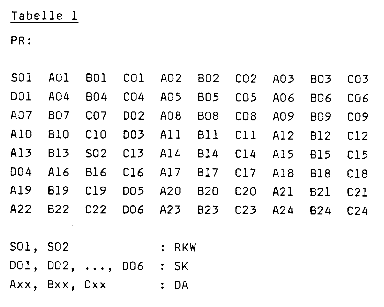
- a suitable pulse frame PR which was specified by Nyhoff, is shown in part in FIG.
- the pulse frame contains 80 code words with 8 bits each. Each of these bytes is labeled.
- the first byte SO1 and another byte SO2 are used for synchronization.
- Other bytes denoted by Dxx are combined to form a signaling channel SK.
- all bytes designated with Axx, Bxx or Cxx are used for the actual data transmission.
- the complete pulse frame - divided into eight lines - is shown in Table 1. If all bytes suitable for data transmission are used for transmission, this results in a transmission rate of 57,600 bit / s.
- This transmission capacity can be divided into three channels K31 to K33 with a transmission rate of 19,200 bit / s each. This division is shown in Table 2.
- up to 6 channels K61 to K66 with 9,600 bit / s each 12 channels K12.1 to K12.12 with 4,800 bit / s each or 24 channels K24 .1 to K24.24 can be formed with 2,400 bit / s each.
- a customary subscriber channel structure is composed of the above-mentioned channels with different data rates.
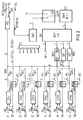
- FIG. 2 shows a flexible multiplex device for 6 subscriber channels CH1 to CH6 and thus also for 6 data terminal devices.
- a serial-to-parallel converter SPU1 to SPU6 is assigned to each subscriber channel, to which the input data are serially supplied via an input E1 to E6.
- the corresponding bit clock BT1 to BT6 is present at the clock input of the serial-parallel converter and is output to the respective data terminal device via clock outputs TA1 to TA6.
- the outputs of the serial-to-parallel converter are connected to a data bus DBM with a word length of 8 bits, which is connected to a parallel-to-serial converter PSU.
- the clock inputs of the serial-parallel converter are connected to a clock supply TVS (not shown) via clock multiplexers CMUX1 to CMUX6. They are controlled by an IFS transmission interface.
- a transmission-side memory controller STS is addressed via a changeover switch US1, the data output of which is controlled via a decoder DEK Selects inputs SE1 to SE6 of the serial-to-parallel converter and the three word generators WG1 to WG3, whose outputs can also be switched to the data bus DBM.
- the distribution of the available transmission capacity among the individual subscriber channels is carried out by programming the memory controller STS, which is designed, for example, as RAM.
- the decoder DEK1 converts the binary input data into one of nine possible output signals to its decoder output DA1, i.e. only one of its nine outputs is active at a time and therefore only switches one of the serial-to-parallel converters or a word generator on the data bus.
- the coding can of course also be taken over directly by the memory controller, but then the word width would then also have to be expanded from four to nine bits.
- the clock supply not only supplies the multiplex signal clock TMS, but also the bit clocks BT derived therefrom and the word clock WT1 for the address counter CNT.
- the counting capacity of the address counter coincides with the number of data words of the pulse frame according to Table 1, so here it includes the counter positions 0 to 79 (mod 80).
- the first frame identifier word SO1 is first output to the parallel-serial converter by the second word generator WG2, converted into serial data and output at the multiplexer output MA.
- the address counter then increases the address SA1 of the memory controller STS by 1, whereupon the first data word in the time slot AO1 is taken over from the first serial-to-parallel converter SPU1.
- the transfer takes place with the corresponding select signal sel1, so that an original byte structure at the output of the first serial-to-parallel converter 1 is generally lost.
- the same assignment takes place again in the demultiplexing device, so that transparent data transmission is ensured.
- a data byte of the second serial-to-parallel converter SPU2 is taken over and transmitted by the parallel-to-serial converter PSU via the data bus DBM, etc
- Table 6 shows a breakdown of five subscriber channels with different speeds.
- Table 7 shows the associated addressing of the memory locations in hexadecimal notation.
- the serial-to-parallel converters each contain a shift register and a memory register, in each of which one byte is stored. Since the time slots of the pulse frame are divided evenly between the different subscriber channels, the transfer to the parallel-serial converter is easy.
- Each serial-parallel converter contains the correct bit clock via a clock multiplexer CMUX1 to CMUX6 which was selected by an interface IFS from four different clock signals with a frequency between 2.4 and 19.2 kHz.
- the interface is programmed according to the STS memory controller. Any register or an output port of a microcomputer can be used as an interface.
- the address input of the memory controller and its data input (not shown in FIG. 2) are connected to a programming device PE and, like the interface, is loaded with the corresponding data.
- the subscriber channel structure and the assignment of the channels to time slots in the pulse frame PR can be determined by a central network controller.
- microcomputer can be interposed as a programming unit PE, which loads the corresponding data into the memory controller STS, STE.
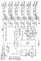
- a demultiplexing device is shown in FIG.
- the received multiplex signal MS is fed to a serial-to-parallel converter SPU via a multiplexer input ME and simultaneously to the data inputs from the parallel-to-serial converters PSU1 to PSU6 via a data bus DBD.
- the serial outputs of the parallel-serial converter form the data outputs A1 to A6.
- Bit clock signals of different frequencies are fed from a receiving clock supply TVE via clock multiplexers CMUX11 to CMUX16 to a clock input of a parallel-serial converter and at the same time via assigned clock outputs TA11 to TA16 delivered.
- the multiplexers are controlled accordingly via a receiving interface IFE.
- the memory controller STE at the receiving end and the associated decoder DEK2 are constructed in accordance with the multiplexing device.
- a second address counter CNT2 is in turn connected to the memory controller STE via a second changeover switch US2.
- the memory controller STE can be switched on to the programming device PE via this switch.
- the demultiplexing device requires synchronization SYNC.
- the multiplex signal is fed to two comparison devices VE1 and VE2 which, when a frame code word SO1 or SO2 is present, emit a corresponding signal to the synchronization, which then enables the address counter CNT2. In order to avoid incorrect synchronization, all known frame synchronization methods can be used.
- SR which is also connected to the data bus DBD and into which the data is transferred under the control of the decoder.
- the multiplex signal MS received at the demultiplexer input DE is fed to the serial-parallel converter SPU with a receive clock TME and converted into parallel data words.
- This parallelized multiplex signal is supplied via the data bus DBD to all parallel-serial converters PSU1 to PSU6.
- the corresponding data words are then controlled by the receive-side memory controller STE - controlled by the selective signals sel11 to sel16 led to the selective inputs SE11 to SE16 by the parallel-serial converters PSU1 to PSU6 taken over and converted again into a continuous serial data stream for each subscriber channel CH1 to CH6.
- the receive-side memory controller STE will be programmed accordingly to the transmit-side memory controller STS.
- a subscriber channel CH1 assigned to the data input D1 in the demultiplexing device may assign another data output, for example data output A4.
- the words of the signaling channel are transferred directly to the signaling register SR and can be called up in parallel at the signaling output SA. If necessary, the conversion can also take place here via a further parallel-serial converter into a serial data stream.
- the same clock supply is used for the multiplexing and demultiplexing device, which then generates all word and bit clock signals.
Abstract
Description
Die Erfindung betrifft ein flexibles Multiplexsystem mit einer Multiplexeinrichtung und einer Demultiplexeinrichtung nach den Oberbegriffen der Patentansprüche 1 und 2.The invention relates to a flexible multiplex system with a multiplex device and a demultiplex device according to the preambles of
Die Multiplex- und die Demultiplexeinrichtung sind insbesondere für ein konfigurierbares Festnetz mit einer Übertragungsbitrate von 64 kbit/s ausgelegt. Davon unabhängig kann das Prinzip der Multiplex- und Demultiplexeinrichtung bei beliebigen Systemen verwendet werden.The multiplex and the demultiplex device are designed in particular for a configurable fixed network with a transmission bit rate of 64 kbit / s. Regardless of this, the principle of the multiplexing and demultiplexing device can be used in any system.
Aus der europäischen Patentanmeldung EP 0 176 148 A2 ist eine Schaltungsanordnung zum Erzeugen eines Zeitmultiplexsignals bekannt, bei denen durch Seriell-Parallel-Wandler die Signale der Eingangsleitungen in parallele Signale umgesetzt werden, die einem Parallel-Seriell-Wandler zur Bildung des Multiplexsignals zugeführt werden. Eine Verarbeitung von Eingangssignalen mit unterschiedlichen Taktraten ist nicht vorgesehen.A circuit arrangement for generating a time-division multiplex signal is known from European patent application EP 0 176 148 A2, in which the signals of the input lines are converted into parallel signals by serial-parallel converters, which are fed to a parallel-serial converter to form the multiplex signal. Processing of input signals with different clock rates is not provided.
Anstelle der bekannten festen Zuordnung von Kanälen mit festen Übertragungsbitraten tritt häufig der Wunsch nach größerer Flexibilität, die es ermöglicht Datenendeinrichtungen mit unterschiedlichen Datenraten an Multiplexeinrichtungen anzuschließen. Es sind rechnergesteuerte Systeme bekannt, die eine solche Flexibilität ermöglichen. Diese Systeme sind jedoch äußerst aufwendig und eignen sich wenig für Einrichtungen bei Teilnehmern, denen beispielsweise ein Anschluß in einem Festnetz zur Verfügung steht.Instead of the known fixed assignment of channels with fixed transmission bit rates, there is often a desire for greater flexibility, which enables data terminal devices with different data rates to be connected to multiplexing devices. Computer-controlled systems are known which allow such flexibility. However, these systems are extremely complex and are not very suitable for facilities for subscribers, for example a connection in a fixed network is available.
Aufgabe der Erfindung ist es, eine flexible Multiplexeinrichtung und eine entsprechende Demultiplexeinrichtung mit geringem Aufwand für ein Multiplexsystem anzugeben.The object of the invention is to provide a flexible multiplex device and a corresponding demultiplex device with little effort for a multiplex system.
Diese Aufgabe wird durch die Merkmale der unabhängigen Ansprüche gelöst.This object is solved by the features of the independent claims.
Vorteilhaft ist die einfache und die flexible durch einen Speicher steuerbare Teilnehmerkanalstruktur. Durch den Decoder wird die Funktionssicherheit, da nur stets ein Datenausgang aus den Datenbus geschaltet werden kann, noch verbessert und der Speicheraufwand noch verringert werden. Mit der Aufteilung des Multiplexkanals in bestimmte Teilnehmerkanäle ergibt sich automatisch die Bitrate für jeden Teilnehmerkanal und ein zugeordneter Bittakt, der über Taktmultiplexer von einer zentralen Taktversorgung durchgeschaltet wird. Voraussetzung ist, daß stets ein geeigneter fester Pulsrahmen vorgegeben ist.The simple and flexible subscriber channel structure that can be controlled by a memory is advantageous. Functional reliability is improved by the decoder, since only one data output can always be switched from the data bus, and the amount of memory is still increased be reduced. The division of the multiplex channel into certain subscriber channels automatically results in the bit rate for each subscriber channel and an assigned bit clock, which is switched through by a central clock supply via clock multiplexers. The prerequisite is that a suitable fixed pulse frame is always specified.
Vorteilhaft ist die Seriell-Parallel-Umsetzung der Eingangsdaten. Hierdurch ergibt sich eine automatische Zwischenspeicherung, die einen übersichtlichen Aufbau mit Hilfe eines Datenbusses ermöglicht.The serial-parallel conversion of the input data is advantageous. This results in an automatic intermediate storage, which enables a clear structure with the help of a data bus.
Der flexible Demultiplexer ist entsprechend aufgebaut. Es kommt lediglich die Synchronisierung hinzu. Die Demultiplexeinrichtung kann unabhängig von der Multiplexeinrichtung aufgebaut werden. Hierdurch ist auch ein Rangieren der Kanäle zwischen beliebigen Eingängen der Multiplexeinrichtung und Ausgängen der Demultiplexeinrichtung möglich.The flexible demultiplexer is designed accordingly. Only the synchronization is added. The demultiplexing device can be constructed independently of the multiplexing device. This also enables the channels to be routed between any inputs of the multiplex device and outputs of the demultiplex device.
Weitere vorteilhafte Ausbildungen sind in den Unteransprüchen angegeben.Further advantageous developments are specified in the subclaims.
Ein Ausführungsbeispiel der Erfindung wird anhand von Figuren und Tabellen näher erläutert.
Es zeigen:
- Fig. 1
- einen Multiplexrahmen,
- Fig. 2
- eine flexible Multiplexeinrichtung und
- Fig. 3
- eine flexible Demultiplexeinrichtung.
Show it:
- Fig. 1
- a multiplex frame,
- Fig. 2
- a flexible multiplexing device and
- Fig. 3
- a flexible demultiplexing device.
In Figur 1 ist ein geeigneter Pulsrahmen PR, der von Nyhoff angegeben wurde, auszugsweise dargestellt. Der Pulsrahmen beinhaltet 80 Codewörter mit jeweils 8 Bits. Jedes dieser Bytes ist bezeichnet. Das erste Byte SO1 und ein weiteres Byte SO2 dienen zur Synchronisation. Andere mit Dxx bezeichnete Bytes sind zu einem Signalisierungskanal SK zusammengefaßt. Dagegen dienen alle mit Axx, Bxx oder Cxx bezeichneten Bytes der eigentlichen Datenübertragung.A suitable pulse frame PR, which was specified by Nyhoff, is shown in part in FIG. The pulse frame contains 80 code words with 8 bits each. Each of these bytes is labeled. The first byte SO1 and another byte SO2 are used for synchronization. Other bytes denoted by Dxx are combined to form a signaling channel SK. In contrast, all bytes designated with Axx, Bxx or Cxx are used for the actual data transmission.
Der vollständige Pulsrahmen - aufgeteilt in acht Zeilen - ist in Tabelle 1 dargestellt. Werden sämtlich zur Datenübertragung geeigneten Bytes zur Übertragung genutzt, so ergibt dies eine Übertragungsrate von 57.600 bit/s. Diese Übertragungskapazität kann auf drei Kanäle K31 bis K33 mit einer Übertragungsrate von jeweils 19.200 bit/s aufgeteilt werden. Diese Aufteilung ist in Tabelle 2 dargestellt. Durch Verringerung der Datenrate je Kanal können nach den weiteren Tabellen 3, 4 und 5 bis zu 6 Kanäle K61 bis K66 mit je 9.600 bit/s, 12 Kanäle K12.1 bis K12.12 mit je 4.800 bit/s oder auch 24 Kanäle K24.1 bis K24.24 mit jeweils 2.400 bit/s gebildet werden. Eine übliche Teilnehmerkanalstruktur setzt sich aus den vorstehend angeführten Kanälen mit unterschiedlichen Datenraten zusammen.The complete pulse frame - divided into eight lines - is shown in Table 1. If all bytes suitable for data transmission are used for transmission, this results in a transmission rate of 57,600 bit / s. This transmission capacity can be divided into three channels K31 to K33 with a transmission rate of 19,200 bit / s each. This division is shown in Table 2. By reducing the data rate per channel, according to the other tables 3, 4 and 5, up to 6 channels K61 to K66 with 9,600 bit / s each, 12 channels K12.1 to K12.12 with 4,800 bit / s each or 24 channels K24 .1 to K24.24 can be formed with 2,400 bit / s each. A customary subscriber channel structure is composed of the above-mentioned channels with different data rates.
Im allgemeinen wird man sich in den Multiplex- und Demultiplexeinrichtungen auf eine geringe Zahl - ca. 4 bis 10 - von Anschlußmöglichkeiten für Datenendeinrichtungen bei einem ISDN-Basisanschluß beschränken. In Figur 2 ist eine flexible Multiplexeinrichtung für 6 Teilnehmerkanäle CH1 bis CH6 und damit auch für 6 Datenendeinrichtungen dargestellt. Jedem Teilnehmerkanal ist ein Seriell-Parallel-Umsetzer SPU1 bis SPU6 zugeordnet, dem die Eingangsdaten jeweils über einen Eingang E1 bis E6 seriell zugeführt werden. Der entsprechende Bittakt BT1 bis BT6 liegt jeweils am Takteingang der Seriell-Parallel-Umsetzer an und wird über Taktausgänge TA1 bis TA6 an die jeweilige Datenendeinrichtung abgegeben. Die Ausgänge der Seriell-Parallel-Umsetzer sind auf einen Datenbus DBM mit einer Wortbreite von 8 Bits geschaltet, der an einen Parallel-Seriell-Umsetzer PSU angeschaltet ist. Die Takteingänge der Seriell-Parallel-Umsetzer sind über Taktmultiplexer CMUX1 bis CMUX6 mit einer nicht dargestellten Taktversorgung TVS verbunden. Gesteuert werden sie von einem sendeseitigen Interface IFS. Über einen mit dem Worttakt WT1 arbeitenden Adressenzähler CNT1 wird über einen Umschalter US1 eine sendeseitige Speichersteuerung STS adressiert, deren Datenausgang über einen Decoder DEK die Selekteingänge SE1 bis SE6 der Seriell-Parallel-Umsetzer und der drei Wortgeneratoren WG1 bis WG3 steuert, deren Ausgänge ebenfalls auf den Datenbus DBM schaltbar sind.In general, the multiplexing and demultiplexing equipment will be limited to a small number - approximately 4 to 10 - of connection options for data terminal equipment with an ISDN basic access. FIG. 2 shows a flexible multiplex device for 6 subscriber channels CH1 to CH6 and thus also for 6 data terminal devices. A serial-to-parallel converter SPU1 to SPU6 is assigned to each subscriber channel, to which the input data are serially supplied via an input E1 to E6. The corresponding bit clock BT1 to BT6 is present at the clock input of the serial-parallel converter and is output to the respective data terminal device via clock outputs TA1 to TA6. The outputs of the serial-to-parallel converter are connected to a data bus DBM with a word length of 8 bits, which is connected to a parallel-to-serial converter PSU. The clock inputs of the serial-parallel converter are connected to a clock supply TVS (not shown) via clock multiplexers CMUX1 to CMUX6. They are controlled by an IFS transmission interface. Via an address counter CNT1 working with the word clock WT1, a transmission-side memory controller STS is addressed via a changeover switch US1, the data output of which is controlled via a decoder DEK Selects inputs SE1 to SE6 of the serial-to-parallel converter and the three word generators WG1 to WG3, whose outputs can also be switched to the data bus DBM.
Die Aufteilung der zur Verfügung stehenden Übertragungskapazität auf die einzelnen Teilnehmerkanäle erfolgt durch Programmierung der Speichersteuerung STS, die beispielsweise als RAM ausgebildet ist. Der Decoder DEK1 setzt die binären Eingangsdaten in eins von neun möglichen Ausgangssignalen an seinen Dekoderausgang DA1 um, d.h. es ist jeweils nur einer seiner neun Ausgänge aktiv und schaltet deshalb nur jeweils einen der Seriell-Parallel-Umsetzer oder einen Wortgenerator auf den Datenbus. Die Codierung kann natürlich auch direkt von der Speichersteuerung übernommen werden, jedoch müßte dann die Wortbreite dann ebenfalls von vier auf neun Bits erweitert werden. Die Taktversorgung liefert nicht nur den Multiplexsignaltakt TMS, sondern auch die hiervon abgeleiteten Bittakte BT und den Worttakt WT1 für den Adressenzähler CNT. Die Zählkapazität des Adressenzählers stimmt mit der Anzahl der Datenwörter des Pulsrahmens nach Tabelle 1 überein, umfaßt hier also die Zählerstellungen 0 bis 79 (mod 80).The distribution of the available transmission capacity among the individual subscriber channels is carried out by programming the memory controller STS, which is designed, for example, as RAM. The decoder DEK1 converts the binary input data into one of nine possible output signals to its decoder output DA1, i.e. only one of its nine outputs is active at a time and therefore only switches one of the serial-to-parallel converters or a word generator on the data bus. The coding can of course also be taken over directly by the memory controller, but then the word width would then also have to be expanded from four to nine bits. The clock supply not only supplies the multiplex signal clock TMS, but also the bit clocks BT derived therefrom and the word clock WT1 for the address counter CNT. The counting capacity of the address counter coincides with the number of data words of the pulse frame according to Table 1, so here it includes the counter positions 0 to 79 (mod 80).
Beginnend beim ersten Byte wird zunächst das erste Rahmenkennungswort SO1 an den Parallel-Seriell-Umsetzer vom zweiten Wortgenerator WG2 abgegeben, in serielle Daten umgesetzt und am Multiplexerausgang MA abgegeben. Der Adressenzähler erhöht daraufhin die Adresse SA1 der Speichersteuerung STS um 1, worauf das erste Datenwort in dem Zeitschlitz AO1 aus dem ersten Seriell-Parallel-Umsetzer SPU1 übernommen wird. Die Übernahme erfolgt mit dem entsprechenden Selektsignal sel1, so daß eine ursprüngliche Bytestruktur am Ausgang des ersten Seriell-Parallel-Umsetzers 1 in der Regel verlorengeht. Es erfolgt jedoch in der Demultiplexeinrichtung wieder dieselbe Zuordnung, so daß eine transparente Datenübertragung gewährleistet ist. Nach dem ersten Datenbyte wird ein Datenbyte des zweiten Seriell-Parallel-Umsetzers SPU2 über den Datenbus DBM vom Parallel-Seriell-Umsetzer PSU übernommen und ausgesendet u.s.w.Starting with the first byte, the first frame identifier word SO1 is first output to the parallel-serial converter by the second word generator WG2, converted into serial data and output at the multiplexer output MA. The address counter then increases the address SA1 of the memory controller STS by 1, whereupon the first data word in the time slot AO1 is taken over from the first serial-to-parallel converter SPU1. The transfer takes place with the corresponding select signal sel1, so that an original byte structure at the output of the first serial-to-
In Tabelle 6 ist eine Aufteilung auf fünf Teilnehmerkanäle mit unterschiedlichen Geschwindigkeiten dargestellt. In Tabelle 7 ist die zugehörige Adressierung der Speicherstellen in hexadezimaler Schreibweise angegeben. Die Seriell-Parallel-Umsetzer beinhalten jeweils ein Schieberegister und ein Speicherregister, in das jeweils ein Byte abgespeichert wird. Da die Aufteilung der Zeitschlitze des Pulsrahmens gleichmäßig auf die verschiedenen Teilnehmerkanäle erfolgt, ist die Übernahme in den Parallel-Seriell-Umsetzer problemlos. Jeder Seriell-Parallel-Umsetzer enthält den richtigen Bittakt über einen Taktmultiplexer CMUX1 bis CMUX6 der von einem Interface IFS von vier verschiedenen Taktsignalen mit einer Frequenz zwischen 2,4 und 19,2 kHz ausgewählt wurde. Das Interface wird entsprechend der Speichersteuerung STS programmiert. Als Interface kann ein beliebiges Register oder ein Ausgangsport eines Mikrorechners Verwendung finden.Table 6 shows a breakdown of five subscriber channels with different speeds. Table 7 shows the associated addressing of the memory locations in hexadecimal notation. The serial-to-parallel converters each contain a shift register and a memory register, in each of which one byte is stored. Since the time slots of the pulse frame are divided evenly between the different subscriber channels, the transfer to the parallel-serial converter is easy. Each serial-parallel converter contains the correct bit clock via a clock multiplexer CMUX1 to CMUX6 which was selected by an interface IFS from four different clock signals with a frequency between 2.4 and 19.2 kHz. The interface is programmed according to the STS memory controller. Any register or an output port of a microcomputer can be used as an interface.
Zur Neuprogrammierung wird der Adresseneingang der Speichersteuerung und ihr Dateneingang (in Fig. 2 nicht dargestellt) an eine Programmiereinrichtung PE angeschaltet und wie auch das Interface mit den entsprechenden Daten geladen.For reprogramming, the address input of the memory controller and its data input (not shown in FIG. 2) are connected to a programming device PE and, like the interface, is loaded with the corresponding data.
Die Teilnehmerkanalstruktur und die Zuordnung der Kanäle zu Zeitschlitzen in dem Pulsrahmen PR kann von einer zentralen Netzsteuerung bestimmt werden. Hierbei kann Mikrorechner als Programmiereinheit PE zwischengeschaltet sein, die die entsprechenden Daten in die Speichersteuerung STS, STE lädt.The subscriber channel structure and the assignment of the channels to time slots in the pulse frame PR can be determined by a central network controller. In this case, microcomputer can be interposed as a programming unit PE, which loads the corresponding data into the memory controller STS, STE.
In Figur 3 ist eine Demultiplexeinrichtung dargestellt. Das empfangene Multiplexsignals MS wird über einen Multiplexereingang ME einem Seriell-Parallel-Umsetzer SPU zugeführt und über einen Datenbus DBD gleichzeitig den Dateneingängen von den Parallel-Seriell-Umsetzern PSU1 bis PSU6 zugeführt. Die seriellen Ausgänge der Parallel-Seriell-Umsetzer bilden die Datenausgänge A1 bis A6. Von einer empfangsseitigen Taktversorgung TVE werden Bittaktsignale unterschiedlicher Frequenz über Taktmultiplexer CMUX11 bis CMUX16 jeweils an einen Takteingang eines Parallel-Seriell-Umsetzers geführt und gleichzeitig über zugeordnete Taktausgänge TA11 bis TA16 abgegeben. Die Steuerung der Multiplexer erfolgt entsprechend über ein empfangsseitiges Interface IFE. Die empfangsseitige Speichersteuerung STE und der zugehörige Decoder DEK2 sind entsprechend der Multiplexeinrichtung aufgebaut. Ein zweiter Adressenzähler CNT2 ist wiederum über einen zweiten Umschalter US2 mit der Speichersteuerung STE verbunden. Über diesen Umschalter kann die Speichersteuerung STE an die Programmiereinrichtung PE eingeschaltet werden. Die Demultiplexeinrichtung benötigt eine Synchronisierung SYNC. Das Multiplexsignal wird zwei Vergleichseinrichtungen VE1 und VE2 zugeführt, die bei Vorliegen eines Rahmenkennungswortes SO1 oder SO2 ein entsprechendes Signal an die Synchronisierung abgeben, die dann den Adressenzähler CNT2 freigibt. Um Fehlsynchronisierung zu vermeiden, könnnen alle bekannten Rahmensynchronisationsverfahren eingesetzt werden.A demultiplexing device is shown in FIG. The received multiplex signal MS is fed to a serial-to-parallel converter SPU via a multiplexer input ME and simultaneously to the data inputs from the parallel-to-serial converters PSU1 to PSU6 via a data bus DBD. The serial outputs of the parallel-serial converter form the data outputs A1 to A6. Bit clock signals of different frequencies are fed from a receiving clock supply TVE via clock multiplexers CMUX11 to CMUX16 to a clock input of a parallel-serial converter and at the same time via assigned clock outputs TA11 to TA16 delivered. The multiplexers are controlled accordingly via a receiving interface IFE. The memory controller STE at the receiving end and the associated decoder DEK2 are constructed in accordance with the multiplexing device. A second address counter CNT2 is in turn connected to the memory controller STE via a second changeover switch US2. The memory controller STE can be switched on to the programming device PE via this switch. The demultiplexing device requires synchronization SYNC. The multiplex signal is fed to two comparison devices VE1 and VE2 which, when a frame code word SO1 or SO2 is present, emit a corresponding signal to the synchronization, which then enables the address counter CNT2. In order to avoid incorrect synchronization, all known frame synchronization methods can be used.
Außerdem ist ein Signalisierungsregister SR vorhanden, das ebenfalls an den Datenbus DBD eingeschaltet ist und in das die Daten vom Decoder gesteuert übernommen werden.There is also a signaling register SR, which is also connected to the data bus DBD and into which the data is transferred under the control of the decoder.
Das am Demultiplexereingang DE empfangene Multiplexsignal MS wird mit einem Empfangstakt TME dem Seriell-Parallel-Umsetzer SPU zugeführt und in parallele Datenwörter umgesetzt. Dies parallelisierte Multiplexsignal wird über den Datenbus DBD allen Parallel-Seriell-Umsetzern PSU1 bis PSU6 zugeführt. Je nach der Struktur der Teilnehmerkanäle CH1 bis CH6 werden dann von der empfangsseitigen Speichersteuerung STE die entsprechenden Datenwörter - durch an die Selekteingänge SE11 bis SE16 der Parallel-Seriell-Umsetzer geführte Selektsignale sel11 bis sel16 gesteuert - von den Parallel-Seriell-Umsetzern PSU1 bis PSU6 übernommen und wieder für jeden Teilnehmerkanal CH1 bis CH6 in einen kontinuierlichen seriellen Datenstrom umgesetzt. Im allgemeinen wird die empfangsseitige Speichersteuerung STE der sendeseitigen Speichersteuerung STS entsprechend programmiert sein. Es ist jedoch auch möglich einen dem Dateneingang D1 zugeordneten Teilnehmerkanal CH1 bei der Demultiplexeinrichtung einem anderen Datenausgang, beispielsweise dem Datenausgang A4, zuzuordnen.The multiplex signal MS received at the demultiplexer input DE is fed to the serial-parallel converter SPU with a receive clock TME and converted into parallel data words. This parallelized multiplex signal is supplied via the data bus DBD to all parallel-serial converters PSU1 to PSU6. Depending on the structure of the subscriber channels CH1 to CH6, the corresponding data words are then controlled by the receive-side memory controller STE - controlled by the selective signals sel11 to sel16 led to the selective inputs SE11 to SE16 by the parallel-serial converters PSU1 to PSU6 taken over and converted again into a continuous serial data stream for each subscriber channel CH1 to CH6. In general, the receive-side memory controller STE will be programmed accordingly to the transmit-side memory controller STS. However, it is also possible for a subscriber channel CH1 assigned to the data input D1 in the demultiplexing device to assign another data output, for example data output A4.
Die Wörter des Signalisierungskanals werden direkt in das Signalisierungsregister SR übernommen und können parallel am Signalisierungsausgang SA abgerufen werden. Im Bedarfsfall kann auch hier die Umsetzung über einen weiteren Parallel-Seriell-Umsetzer in einen seriellen Datenstrom erfolgen.The words of the signaling channel are transferred directly to the signaling register SR and can be called up in parallel at the signaling output SA. If necessary, the conversion can also take place here via a further parallel-serial converter into a serial data stream.
In der Regel wird dieselbe Taktversorgung für die Multiplex- und Demultiplexeinrichtung verwendet, die dann sämtliche Wort- und Bittaktsignale erzeugt.


Claims (7)
- Flexible multiplex system with multiplexing equipment which has a plurality of data inputs (E1, E2, ...) for connecting data terminal equipment and a multiplexer for forming a multiplex signal (MS), there being assigned to each data input (E1 to E6) a serial-parallel converter (SPU1 to SPU6), the parallel outputs of which are connected to a data bus (DBM), to which there are also connected the inputs of a parallel-serial converter (PSU) which emits the multiplex signal (MS) at its output, characterized in that a memory controller (STS) on the transmitting side is provided, the memory address (SA1) of which is changed step by step by means of an address counter (CNT1), in that the output data of the memory controller are converted into select signals (sel 1 to sel 6) which control the data transfer of the serial-parallel converters (SPU1 to SPU6) by means of their select inputs (SE1 to SE6) in accordance with an intended subscriber channel configuration, and in that the bit clock signal (BT1 to BT6) which corresponds to the respective subscriber channel (CH1 to CH6) is fed by a clock supply (TVS), which emits bit clock signals having a plurality of different frequencies, to each serial-parallel converter (SPU1 to SPU6) by means of clock multiplexers (CMUX1 to CMUX6).
- Flexible multiplex system with demultiplexing equipment which has a plurality of data outputs (A1 to A6) for connecting data terminals, which has a demultiplexer for splitting a multiplex signal (MS) between different subscriber channels (CH1 to CH6) and in the case of which a synchronization device (SYNC) is provided, the received multiplex signal (MS) being fed to a serial-parallel converter (SPU) and the parallel outputs of the serial-parallel converter (SPU) being led via a data bus (DBD) to the parallel inputs of parallel-serial converters (PSU1 to PSU6), the data acceptance of which can be activated by means of select inputs (SE11 to SE16), characterized in that a memory controller (STE) on the receiving side is provided, the memory address (SA2) of which is changed step by step by means of a second address counter (CNT2) and the output data of which are converted into select signals (sel 11 to sel 16) which control the parallel-serial converters (PSU1 to PSU6) in accordance with a chosen subscriber channel configuration, in that the bit clock signal (BT11 to BT16) which corresponds to the respective subscriber channel (CH1 to CH6) is fed by a clock supply (TVE), which emits bit clock signals having a plurality of different frequencies, to each parallel-serial converter (PSU1 to PSU6) by means of clock multiplexers (CMUX11 to CMUX16).
- Flexible multiplex system according to Claim 1 or 2, characterized in that a decoder (DEK1, DEK2) is connected to the outputs of the memory controller (STS, STE), which decoder in each case emits an active logic signal at only one of its outputs (DA1, DA2).
- Flexible multiplex system according to one of the preceding claims, characterized in that the address counter (CNT1, CNT2) has in each case a counting range which corresponds to the range of words of the pulse frame (PR).
- Flexible multiplex system according to one of the preceding claims, characterized in that the memory controller (STS, STE) is programmable or exchangeable, and a correspondingly programmable, adjustable or exchangeable interface (IFS, IFE) is provided for controlling the clock multiplexers (CMUX1 to CMUX6, CMUX11 to CMUX16).
- Flexible multiplex system according to one of the preceding claims, characterized in that the serial-parallel converters (SPU1 to SPU6) and respectively the parallel-serial converters (PSU1 to PSU6) have in each case a memory register for the data words which are present in parallel form.
- Flexible multiplex system according to one of the preceding claims, characterized in that the multiplex signal (MS) has a data rate of 64 kbit/s, in that the pulse frame contains 80 bytes, and in that 4 to 10 subscriber channels (CH1, CH2,...) are provided.
Applications Claiming Priority (2)
| Application Number | Priority Date | Filing Date | Title |
|---|---|---|---|
| DE4007818 | 1990-03-12 | ||
| DE4007818 | 1990-03-12 |
Publications (3)
| Publication Number | Publication Date |
|---|---|
| EP0446441A2 EP0446441A2 (en) | 1991-09-18 |
| EP0446441A3 EP0446441A3 (en) | 1991-11-21 |
| EP0446441B1 true EP0446441B1 (en) | 1995-04-26 |
Family
ID=6402010
Family Applications (1)
| Application Number | Title | Priority Date | Filing Date |
|---|---|---|---|
| EP90123452A Expired - Lifetime EP0446441B1 (en) | 1990-03-12 | 1990-12-06 | Flexible multiplex system |
Country Status (4)
| Country | Link |
|---|---|
| EP (1) | EP0446441B1 (en) |
| AT (1) | ATE121888T1 (en) |
| DE (1) | DE59008974D1 (en) |
| NO (1) | NO910960L (en) |
Families Citing this family (1)
| Publication number | Priority date | Publication date | Assignee | Title |
|---|---|---|---|---|
| DE19730623A1 (en) | 1997-07-17 | 1999-01-21 | Alsthom Cge Alcatel | Method for allocating time slots, as well as system, center and subscriber facility for performing this method |
Family Cites Families (2)
| Publication number | Priority date | Publication date | Assignee | Title |
|---|---|---|---|---|
| GB2128450B (en) * | 1982-10-04 | 1986-01-29 | Hitachi Ltd | Time-division switching unit |
| DE3435652A1 (en) * | 1984-09-28 | 1986-04-10 | Philips Patentverwaltung Gmbh, 2000 Hamburg | CIRCUIT ARRANGEMENT FOR GENERATING A TIME MULTIPLEX SIGNAL |
-
1990
- 1990-12-06 EP EP90123452A patent/EP0446441B1/en not_active Expired - Lifetime
- 1990-12-06 AT AT90123452T patent/ATE121888T1/en active
- 1990-12-06 DE DE59008974T patent/DE59008974D1/en not_active Expired - Fee Related
-
1991
- 1991-03-11 NO NO91910960A patent/NO910960L/en unknown
Also Published As
| Publication number | Publication date |
|---|---|
| DE59008974D1 (en) | 1995-06-01 |
| EP0446441A2 (en) | 1991-09-18 |
| NO910960D0 (en) | 1991-03-11 |
| ATE121888T1 (en) | 1995-05-15 |
| NO910960L (en) | 1991-09-13 |
| EP0446441A3 (en) | 1991-11-21 |
Similar Documents
| Publication | Publication Date | Title |
|---|---|---|
| DE2848255C2 (en) | ||
| EP1280373B1 (en) | Networkelement for optical transport network signals | |
| DE2714368C3 (en) | Circuit arrangement for switching through data words with different bit rate frequencies in multiple connections | |
| EP0598455B1 (en) | Transmission system for synchronous digital hierarchy | |
| EP0007524A1 (en) | Method and circuit for data transmission | |
| DE2520835C3 (en) | Circuit arrangement for the transmission of synchronously and asynchronously occurring data | |
| EP0446441B1 (en) | Flexible multiplex system | |
| DE602004012066T2 (en) | Time-multiplexed links between a switching matrix and a port in a network element | |
| EP0103163B1 (en) | Device for synchronously demultiplexing a time division multiplex signal | |
| EP0765050A2 (en) | Method for controlling the transmission of digital communication signals via a time division multiplex medium | |
| WO1998001971A1 (en) | Network element and input-output unit for a synchronous transmission system | |
| DE69738078T2 (en) | SYSTEM AND METHOD FOR TIMING CONTROL IN A DISTRIBUTED CROSS-CONCRETE DIGITAL SYSTEM | |
| DE3501674A1 (en) | Multiplexer/demultiplexer with flexible signal processing function for digital time-division multiplex communications systems | |
| EP0143268A2 (en) | Process and device for inserting a digital binary narrow-band signal in, or for extracting this norrow-band signal from a time division multiplex signal | |
| DE3107046C2 (en) | ||
| EP0110360B1 (en) | Circuit arrangement for composing and separating speech and data during the transmission in a digital switching network | |
| EP0565890A2 (en) | Method and system for the transmission of a data signal in a VC-12-container in transmission channels | |
| EP0324954A2 (en) | Method and device for the shared transmission of digitized television, sound and data signals | |
| EP0176148A2 (en) | Circuit for the generation of a time division multiplex signal | |
| AT390703B (en) | CONVERTER CIRCUIT FOR INTERMEDIATING BETWEEN DIGITAL AND PULSAMPLITUDE-MODULATED SIGNALS AND FOR SELECTING MODIFICATION OF THE DIGITAL SIGNALS | |
| DE69736716T2 (en) | DISTRIBUTED DIGITAL CROSS CONNECT SYSTEM AND METHOD | |
| EP0033122A1 (en) | Process and circuit arrangement for the transmission of data in a synchronous data network | |
| DE4129543C1 (en) | Transmission of async. additional data over audio channels in time multiplex system - adding data to some of audio channels and inputting to multiplexer receiving signals from other channels handling only audio signals | |
| DE10065001A1 (en) | Optical crossconnect for the optional interconnection of message signals of different multiplex levels | |
| DE4309778C1 (en) | Method and arrangement for inserting a 34 Mbit/s signal into D39 pulse frames |
Legal Events
| Date | Code | Title | Description |
|---|---|---|---|
| PUAI | Public reference made under article 153(3) epc to a published international application that has entered the european phase |
Free format text: ORIGINAL CODE: 0009012 |
|
| 17P | Request for examination filed |
Effective date: 19901220 |
|
| AK | Designated contracting states |
Kind code of ref document: A2 Designated state(s): AT BE CH DE LI NL |
|
| PUAL | Search report despatched |
Free format text: ORIGINAL CODE: 0009013 |
|
| AK | Designated contracting states |
Kind code of ref document: A3 Designated state(s): AT BE CH DE LI NL |
|
| 17Q | First examination report despatched |
Effective date: 19940117 |
|
| GRAA | (expected) grant |
Free format text: ORIGINAL CODE: 0009210 |
|
| AK | Designated contracting states |
Kind code of ref document: B1 Designated state(s): AT BE CH DE LI NL |
|
| REF | Corresponds to: |
Ref document number: 121888 Country of ref document: AT Date of ref document: 19950515 Kind code of ref document: T |
|
| REF | Corresponds to: |
Ref document number: 59008974 Country of ref document: DE Date of ref document: 19950601 |
|
| PG25 | Lapsed in a contracting state [announced via postgrant information from national office to epo] |
Ref country code: AT Effective date: 19951206 |
|
| PG25 | Lapsed in a contracting state [announced via postgrant information from national office to epo] |
Ref country code: LI Effective date: 19951231 Ref country code: CH Effective date: 19951231 Ref country code: BE Effective date: 19951231 |
|
| PLBE | No opposition filed within time limit |
Free format text: ORIGINAL CODE: 0009261 |
|
| STAA | Information on the status of an ep patent application or granted ep patent |
Free format text: STATUS: NO OPPOSITION FILED WITHIN TIME LIMIT |
|
| 26N | No opposition filed | ||
| BERE | Be: lapsed |
Owner name: SIEMENS A.G. Effective date: 19951231 |
|
| REG | Reference to a national code |
Ref country code: CH Ref legal event code: PL |
|
| PGFP | Annual fee paid to national office [announced via postgrant information from national office to epo] |
Ref country code: DE Payment date: 19980220 Year of fee payment: 8 |
|
| PGFP | Annual fee paid to national office [announced via postgrant information from national office to epo] |
Ref country code: NL Payment date: 19981217 Year of fee payment: 9 |
|
| PG25 | Lapsed in a contracting state [announced via postgrant information from national office to epo] |
Ref country code: DE Free format text: LAPSE BECAUSE OF NON-PAYMENT OF DUE FEES Effective date: 19991001 |
|
| PG25 | Lapsed in a contracting state [announced via postgrant information from national office to epo] |
Ref country code: NL Free format text: LAPSE BECAUSE OF NON-PAYMENT OF DUE FEES Effective date: 20000701 |
|
| NLV4 | Nl: lapsed or anulled due to non-payment of the annual fee |
Effective date: 20000701 |