EP0444885B1 - A method for controlling a buffer memory for a magnetic disk storage system - Google Patents
A method for controlling a buffer memory for a magnetic disk storage system Download PDFInfo
- Publication number
- EP0444885B1 EP0444885B1 EP91301553A EP91301553A EP0444885B1 EP 0444885 B1 EP0444885 B1 EP 0444885B1 EP 91301553 A EP91301553 A EP 91301553A EP 91301553 A EP91301553 A EP 91301553A EP 0444885 B1 EP0444885 B1 EP 0444885B1
- Authority
- EP
- European Patent Office
- Prior art keywords
- bit
- address
- error detection
- detection code
- buffer memory
- Prior art date
- Legal status (The legal status is an assumption and is not a legal conclusion. Google has not performed a legal analysis and makes no representation as to the accuracy of the status listed.)
- Expired - Lifetime
Links
Images


Classifications
-
- G—PHYSICS
- G06—COMPUTING OR CALCULATING; COUNTING
- G06F—ELECTRIC DIGITAL DATA PROCESSING
- G06F11/00—Error detection; Error correction; Monitoring
- G06F11/07—Responding to the occurrence of a fault, e.g. fault tolerance
- G06F11/08—Error detection or correction by redundancy in data representation, e.g. by using checking codes
- G06F11/10—Adding special bits or symbols to the coded information, e.g. parity check, casting out 9's or 11's
- G06F11/1008—Adding special bits or symbols to the coded information, e.g. parity check, casting out 9's or 11's in individual solid state devices
-
- G—PHYSICS
- G06—COMPUTING OR CALCULATING; COUNTING
- G06F—ELECTRIC DIGITAL DATA PROCESSING
- G06F3/00—Input arrangements for transferring data to be processed into a form capable of being handled by the computer; Output arrangements for transferring data from processing unit to output unit, e.g. interface arrangements
- G06F3/06—Digital input from, or digital output to, record carriers, e.g. RAID, emulated record carriers or networked record carriers
- G06F3/0601—Interfaces specially adapted for storage systems
- G06F3/0628—Interfaces specially adapted for storage systems making use of a particular technique
- G06F3/0655—Vertical data movement, i.e. input-output transfer; data movement between one or more hosts and one or more storage devices
- G06F3/0656—Data buffering arrangements
Definitions
- Temporary storage devices such as dynamic random access memory (DRAM) devices are often used in connection with magnetic storage media as buffer memories for temporarily storing character information.
- Each character is represented, for example, by an 8-bit information word and 1-parity bit.
- information is read into a temporary storage memory device one character at a time using nine parallel data bit lines.
- DRAMs are typically available as 4- or 1-bit wide devices, so that storage of the extra parity bit associated with each information word is cumbersome, resulting in the parity bit not being stored or being stored in a separate memory device.
- a SECTOR/WAM/AMD signal on a line 30 is a sector input, address mark detected input, or write address mark output to or from the formatter 14, depending on the operating mode of the system.
- the formatter 14 also contains an error correction code circuit ECC 32. Signals passing between the memory control unit 12 and the formatter 14 are carried on a signal bus 34.
Landscapes
- Engineering & Computer Science (AREA)
- Theoretical Computer Science (AREA)
- Physics & Mathematics (AREA)
- General Engineering & Computer Science (AREA)
- General Physics & Mathematics (AREA)
- Quality & Reliability (AREA)
- Human Computer Interaction (AREA)
- Indexing, Searching, Synchronizing, And The Amount Of Synchronization Travel Of Record Carriers (AREA)
- Dram (AREA)
- Compression, Expansion, Code Conversion, And Decoders (AREA)
Abstract
Description
- This invention relates to a method for controlling buffer memories for magnetic disk storage systems.
- Temporary storage devices such as dynamic random access memory (DRAM) devices are often used in connection with magnetic storage media as buffer memories for temporarily storing character information. Each character is represented, for example, by an 8-bit information word and 1-parity bit. Typically, information is read into a temporary storage memory device one character at a time using nine parallel data bit lines. DRAMs are typically available as 4- or 1-bit wide devices, so that storage of the extra parity bit associated with each information word is cumbersome, resulting in the parity bit not being stored or being stored in a separate memory device.
- It is an object of the invention to provide a controller for and a method of controlling DRAM buffer memories for a magnetic disk storage system, which permits efficient use of standard low cost DRAM memories for storing information data and parity data in a variety of DRAM memory modes.
- According to the present invention there is provided a method for temporarily storing and retrieving q-bit character information data for an information storage system in a y-bit wide buffer memory unit comprising a plurality of DRAMS, with q being greater than y, characterised by:
- providing a virtual memory address for each item of q-bit character information data, said character information data being organised into a block comprising z said information characters;
- translating the virtual memory addresses into corresponding addresses of memory locations in said buffer memory unit for storage of y-bit groups of said block in said buffer memory unit, said translating step including
- selecting a row address for storage of said block,
- selecting a base column address for said block, and
- successively incrementing said base column address to provide additional column addresses for successive y-bit groups of said block;
- transferring each of said y-bit groups of said block via a y-bit data bus to an address location in said buffer memory unit determined by said translating step;
- providing a x-bit error detection code word for each said block;
- selecting an address for storing said x-bit error detection code word in said buffer memory unit; said selecting an address including:
- selecting an error detection code word row address;
- selecting an error detection code word base column address for a first y-bit group of said x-bit error detection code word;
- incrementing said error detection code word base column address by y to provide a second column address for a second y-bit group of said x-bit error detection code word; and transferring said error detection code word via said y-bit data bus to the selected address locations for said x-bit error detection code word in said buffer memory unit.
-
- In accordance with a preferred embodiment of the present invention, there is provided a method for temporarily storing and retrieving 8-bit character information data for a magnetic disk information storage system in a number of 4xn DRAM buffer memory configurations, characterised by the steps of: providing a virtual memory address for each item of 8-bit character information data, said character information data being organised into a 16-byte block, translating the virtual memory addresses into corresponding addresses of memory locations in said 4xn buffer memory for storage of 4-bit groups of said 16-byte block in said 4xn DRAM buffer memory, said translating step including: selecting a row address for storage of said 16-byte block, selecting a base column address for said 16-byte block, and successively incrementing said base column address to provide additional column addresses for successive 4-bit groups of said 16-byte block, and transferring each of said 4-bit groups of said 16-byte block through a 4-bit data bus to the various pre-determined address locations in one of said 4xn DRAM buffer memory configurations, where n is the size of the 4-bit wide DRAM, e.g. n=32Kb, n=64Kb, n=256Kb, etc, determined by said translating step.
- Advantageously, an error detection code word in the form of an 8-bit parity word is provided for the 16-byte block and is stored by selecting a parity word row address, selecting a parity word base column address for a first 4-bit group of said 8-bit parity word, and incrementing said parity word column address to provide a second column address for a second 4-bit group of said 8-bit parity word. The error detection code word is then transferred through the 4-bit data bus to the various pre-determined address locations in the 4xn buffer memory for said 8-bit parity word.
- The translating step may include selecting row and column addresses using multiplexer circuits. The method may further include the step of latching the row and column addresses into latch circuits, the incrementing step including the step of feeding the outputs of the latch circuits through multiplexing circuits connected to the inputs of the latch circuits to increment the column addresses.
- Optionally, the 4xn buffer memory may comprise a DRAM operating in a page mode or in a static column mode.
- A further object of the invention is solved by the features of
claim 10. - The invention is described further, by way of example, with reference to the accompanying drawings, in which:-
- Figure 1 is an overall functional block diagram of an integrated circuit SCSI controller which includes a DRAM interface circuit for communicating with a DRAM buffer memory over a 4-bit data line;
- Figure 2 is a block diagram of a buffer memory control portion of the SCSI controller;
- Figure 3 is a block diagram of the buffer memory control portion showing the interfaces required to transfer data from a disk memory to a host computer;
- Figure 4 is a block diagram showing storage of character information data and parity data in the buffer memory when data is written from a host computer to a disk memory;
- Figure 5 is a timing diagram for a normal page-mode block transfer of data between the controller and a DRAM buffer memory;
- Figure 6 is a timing diagram for a static-column-mode block transfer of data between the controller and a DRAM buffer memory;
- Figure 7 is a timing diagram for an inter-leaved page-mode block transfer of data between the controller and a DRAM buffer memory;
- Figure 8 is a block diagram of the DRAM interface circuit of the controller;
- Figure 9 is a circuit diagram of a state machine portion of the DRAM interface circuit; and
- Figure 10 is a circuit diagram of an address sequencer portion of the DRAM interface circuit.
-
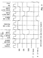
- Figure 1 shows a block diagram of a 68-pin integrated circuit small computer system interface (SCSI)
controller circuit 10. As shown in the diagram, various interfaces are connected by signal buses to amemory control unit 12. Aformatter 14 provides an interface to a magnetic storage disk through various signal lines. An NRZ signal on aline 16 is an input/output signal in an NRZ data format, which provides a data bit stream to or from the logic in theformatter 14. An RD/REF CLK signal on aline 18 is a read/reference clock, which is the clock signal for theformatter 14 supplied by a data separator of the magnetic disk electronics. The frequency of this clock signal ranges from 5 Mhz to 24 Mhz. A read gate signal RG on asignal line 20 is a signal which enables a read channel and causes thecontroller circuit 10 to input NRZ data from the magnetic disk. A write gate signal WG on asignal line 22 is a signal which enables write drivers and causes thecontroller circuit 10 to output NRZ data to the magnetic disk. An INPUT/COAST signal on a line 24 and an OUTPUT signal on a line 26 are general purpose signals used to synchronise theformatter 14 with external hardware. An INDEX signal on a line 28 is an index signal from the magnetic disk drive and is supplied once per revolution of the disk. A SECTOR/WAM/AMD signal on aline 30 is a sector input, address mark detected input, or write address mark output to or from theformatter 14, depending on the operating mode of the system. Theformatter 14 also contains an error correctioncode circuit ECC 32. Signals passing between thememory control unit 12 and theformatter 14 are carried on asignal bus 34. - Communication between the
memory control unit 12 and an external micro-processor, such as an 8051 Intel Controller, is handled with amicro-processor interface circuit 40, which communicates with thememory control circuit 12 through abus 42. An active low chip select signal CS on asignal line 44 enables the controller integratedcircuit 10 for either a read or a write operation. An active low read data signal RD on asignal line 46 in conjunction with the CS signal causes data from a specified register within thememory control circuit 12 to be moved to a data bus AD provided by abus 52, as indicated. The micro-processor address/data bus AD (7:0) is an input/output bus with active high signals provided on bi-directional signal lines, which interface with a multiplexed micro-processor address/data bus of the external micro-processor. An active low write data signal WR on asignal line 48 in connection with the CS signal causes data from the data bus AD to be moved to a specified register within thememory control unit 12. An interrupt request signal IRQ on a signal line 54 is an active low output signal from a micro-processor interfaceinterrupt control circuit 56 to interrupt the external micro-processor. Aclock control circuit 58 within theintegrated circuit 10 provides appropriate clocks to aclock bus 60 to themicro-processor interface circuit 40. Signals from themicro-processor interface circuit 40 to theformatter 14 are provided on abus 62. - An
SCSI interface circuit 70 provides for communication on anSCSI bus 92 from a host computer to thememory control unit 12. Active low input/output signal lines DB (7:0) are the SCSI data lines. An active low input/output busy SCSI control signal BSY is provided on a signal line 74. An active low input/output SCSI SEL control signal is provided on asignal line 76. An active low input/output command/data SCSI control signal C/D is provided on a signal line 78. An active low input/output message SCSI control signal MSG is provided on a signal line 82. An active low input/output request signal REQ in connection with an active low input/output acknowledged signal ACK on a line 86 forms an SCSI data transfer hand shake. An active low input/output SCSI attention control signal ATN is provided on asignal line 88. An active low input/output SCSI re-set signal is provided on a signal line 90. All of the above SCSI control signals are provided in accordance with the SCSI standards. TheSCSI interface circuit 70 is coupled to thememory control circuit 12 through thesignal bus 92. - A
DRAM interface circuit 100 for providing communication with a DRAM buffer memory is coupled to thememory control circuit 12 through asignal bus 101. External connections from theDRAM interface circuit 100 to the DRAM buffer memory are provided through various signal lines. An active low output row address strobe signal RAS on asignal line 102 provides an address strobe for the DRAM buffer memory. An active low input/output column address strobe signal CAS on asignal line 104 provides an address strobe for a first or an only DRAM. A second active low output column address strobe signal CAS2 on asignal line 106 provides an address strobe for a second DRAM. An active low output write strobe signal W is provided on asignal line 108. An active low output enable signal G on asignal line 110 is a DRAM output driver enable signal. Anaddress bus 112 provides nine bits of DRAM address A (8:0). Active high input/output signals are provided on a DRAM data bus DQ (3:0). - Figure 2 shows diagrammatically the interface circuits for the
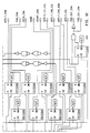
integrated circuit 10. The data is transferred to and from the threebuses DRAM data bus 114. Data from theSCSI data bus 72, that is host data, is input to ahost FIFO 120. Formatted data from theformatter 14 is input to aformat FIFO 122. Read/write data from the microprocessor on thebus 52 is input to awindow RAM 124. Byte/wide data transfers to and from each of these asynchronous interfaces are made to the respective FIFOs. Nibble/wide transfers are made to and from the DRAM between the respective FIFOs under the control of astate machine 126. - Several different DRAM configurations can be implemented, which include: one 4 x 64K DRAM page mode or static column mode; two 4 x 64K DRAMs; one 4 x 256K DRAM page mode or static column mode; and two 4 x 256K DRAMs. The circuit also provides two nibbles of parity for each thirty two nibble transfer. Transfers to and from the DRAM are in blocks of thirty two nibbles, or 16-bytes. An
arbitration circuit 128 gives priority for each interface operation with the DRAM. The disk sequencer for the magnetic disk which provides formatted data from theformat FIFO 122 has the highest priority. Refresh of the DRAM buffer memory has the next highest priority. Data from the micro-processor from the read/write bus, which is stored in thewindow ram 124, has the next highest priority. Finally, host data on theSCSI bus 72 stored in thehost FIFO 120 has the lowest priority. Thearbitration circuit 128 arbitrates at the end of each 16-byte transfer and allows only one interface access to the DRAM at a time. A parity generator/checker circuit 130 provides the two nibbles of parity for each thirty two nibble transfer. - Figure 3 is a block diagram of the buffer memory controller showing the interfaces required to transfer data from a disk memory to a host computer on the SCSI bus. The controller can handle three asynchronous interfaces to the
DRAM buffer memory 130. Figure 3 diagrammatically shows various sectors of theDRAM buffer memory 130 being utilised. As the disk information is filling sector n+2 of theDRAM buffer memory 130 from the disk orformat FIFO 122, the microprocessor can be correcting sector n+1, and the host computer connected to theSCSI bus 72 can be reading sector n through thehost FIFO 120. - Figure 4 diagrammatically shows the storage character information data and parity data in the buffer memory when the data is being written from the
SCSI bus 72 to the disk memory connected to thebus 34. Information from thehost FIFO 120 is input to the DRAM in 16-byte blocks of data. Parity for that block is generated by the parity generator 130a and stored in the parity portion of theDRAM buffer memory 130. For read out, the data is read out from both the parity storage area and the information storage area of theDRAM buffer memory 130 to theform FIFO 122. Parity checking on the output data being read out from theDRAM buffer memory 130 is performed by the parity checker 130b. Parity is generated during the write mode and it is checked during the read mode. Parity is written in a separate place in the DRAM with 2K bytes of address space required for parity for every 32K bytes of total memory. - Figures 5, 6 and 7 show timing diagrams for various DRAM buffer memory configurations to and from which blocks of data are transferred between the
memory control logic 12 and theDRAM buffer memory 130. TheDRAM interface 100 operates on blocks of data, which are 16-bytes in length. All transfers of lesser amounts of data are padded by the control logic prior to theDRAM interface 100 receiving the blocks of information. The buffer control logic also calculates parity, which is two nibbles of longitudinal parity for thirty two nibbles of data. TheDRAM interface 100 performs a remapping of the base address of the information to simplify the internal logic. However, parity is always placed in the top 1/16th of the address space of the DRAM buffer memory as seen from inside. Various sizes of DRAM buffer memory can be used and these sizes include: 32K, 64K, 128K and 256K. One 256K DRAM provides a 32K buffer memory. Two 256K DRAMs provide a 64K buffer memory. One 1M DRAM provides a 128K buffer memory. Two 1M DRAMs provide a 256K buffer memory. - The transfer sequence for a block of data to a normal page mode DRAM is shown in Figure 5. First, the row address is presented. Then thirty two columns of data are transferred. Then, the parity row address is presented followed by the parity information from the two parity columns. Note that if a single page mode DRAM is used, each column of information except the last is followed by a column pre-charge cycle.
- Figure 6 shows the timing signals for a single static-column mode DRAM. If a single static-column mode DRAM is used, the information from a column is transferred one after another with no intervening precharge cycle required. This greatly increases the speed of data transfer. If two DRAM memories are used, they are auto-matically alternated so that a pre-charge cycle for one DRAM occurs at the same time as the column cycle for the other. This results in the same speed as a static-column DRAM would give. Thus there is no advantage in using static-column DRAMs, which are more expensive, in a two RAM configuration. If it is necessary to use static-column DRAMs in a two RAM configuration, these memories can be used in a page mode of operation.
- Figure 7 shows an inter-leaved page mode timing diagram.
- From the timing diagrams, it can be seen that transfer of a single 16-byte block of information in a normal page mode of operation takes 72 cycles of the DRAM clock, while the same transfer in static-column or inter-leaved page mode is 40 cycles of the DRAM clock. With this information, the calculation of the required speed of a DRAM to achieve a buffer band width, as well as the speed of the clock, can be made. For a single page mode DRAM, the minimum cycle time required is equal to the column access time. While for a single static-column DRAM or two page mode DRAMs, the minimum cycle time is equal to the column access time plus an address control skew time. It is recommended that the nominal cycle time be set somewhat slower than the minimum cycle time to allow for speed variations due to voltage ripple on the DRAM power supplies. If a 32K buffer using a single Texas Instruments TMS4464-12 256K page mode DRAM is used, a 60 nS column access time is obtained. The clock is set for a cycle time greater than 61.8 nS. The worst case slow cycle time will be 63.8 nS for a total time of 4,594 nS to transfer a 16-byte block of information or a guaranteed band width of 3.48 megabytes/second. If two 256K page mode DRAMs are used, the clock is set to greater than 64.9 nS with a worst case slow time of 66.9 nS, taking 2,676 nS to transfer a block of information with a guaranteed band width of 5.98 megabytes. If a full 8-megabyte band width is required, a block of information must be transferred every 1,961 nS, allowing for refresh, and the worst case time will be 49 nS. This would require the use of a static-column DRAM or a pair of page mode DRAMS with a column access time less than 45.7 nS.
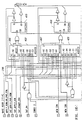
- Figure 8 is a block diagram of a control logic circuit. It shows the main elements of the
DRAM interface circuit 100 of Figure 1. TheDRAM interface circuit 100 includes a control state machine (Control FSM) 200 and anaddress generator 202. Theaddress generator 202 provides the address signals on asignal bus 112 to the DRAM buffer memory. A DRAM clock signal is provided at aninput terminal 204. The DRAM clock signal is distributed to thecontrol state machine 200, theaddress generator 202 and a block of four pairs of D flip flops, one of which is typically shown asreference numeral 206. Each pair of the D flip flops processes, respectively, one bit of four bits of read data, received on asignal bus 208, or write data, received on asignal bus 210. Each of the respective read data bits and write data bits are re-timed with the DRAM clock in respective D flipflops block 206 shows the re-timing circuit for the ith bit. The re-timed read data is re-assembled in adata bus 216 and the re-timed write data is assembled in adata bus 218, as shown. - The
control state machine 200 receives the DRAM clock on asignal line 220. A re-set signal is received on asignal line 222. A start signal is received on asignal line 224. A refresh command signal is received on asignal line 226. A signal indicating that a static column DRAM mode is being used is received on asignal line 230. A signal indicating that two DRAMs are to be used is received on asignal line 232. Thecontrol state machine 200 provides an inverted row address select signal RAS on thesignal line 102; an inverted column address signal CAS on thesignal line 104; a second column address signal CAS2 on thesignal line 106; an inverted DRAM write strobe W on thesignal line 108 and a DRAM output drive enable signal G on thesignal line 110. When 16-bytes of information has been transferred a DONE signal is provided on asignal line 234. - The
address generator 202, as previously mentioned, provides nine address bits on thesignal bus 112 to the DRAM. The address generator includes a counter, which counts from the base address provided as an input to the address generator on asignal line 236. A signal indicating that two DRAMS are being used for buffer storage is provided on asignal line 238. A signal indicating whether one megabit RAMS are being used is provided on asignal line 240. The counters within theaddress generator 202 are enabled by a count enable signal provided from thecontrol state machine 200 on asignal line 242. A signal is output from theaddress generator 202 on asignal line 243 to thecontrol state machine 200 when a count of thirty two is reached in the address generator indicating that the end of a block of data has been reached. - Signals pass between the
control state machine 200 and theaddress generator 202 onsignal lines line 248 steers the multiplexer to form the data row address. A signal Apply_Col on theline 247 tells it to form the data column address. A signal Apply_Par_Row on theline 246 forms the parity row address. A signal Apply_Par_Col on theline 245 forms the parity column address. A signal Apply_1st_Col on theline 244 says that this is the first column address of either the data or parity group, and causes the count bits to be set to zero. A signal Count Ena on theline 242 causes them to count. If the signal Apply_Col or Apply_Par_Col are true, and neither of the signals Apply_1st_Col nor Count_Ena are true, the count bits will be held as they are. If the signal Terminal-Count on theline 243 is the signal back to thecontrol state machine 200 that the count sequence for the data bits is completed, and allows thecontrol state machine 200 to move onto the states in which parity is written or read. - Functionally, the DRAM interface circuit shown in Figure 8 corresponds with the
DRAM interface circuit 100 shown in Figure 1. - Ordinarily, to support a large number of different sizes of DRAMs, it would be required that a large number of addresses be multiplexed by a circuit such as the
address generator 202. However, it is possible to fold the addresses required in such a way that the nubmer of address bits required to provide all of the addresses required for the memory for a given bit can effectively be reduced from nine to approximately four. Table 1 as shown below shows a conventional scheme for providing connections for fourteen bits of internal addresses, designated as IA14 to IA4 (as provided on the signal bus 236) to the DRAM address lines designated A8 to A0 (provided on the address bus 112) to the DRAM. - Table 1 is shown for two DRAM buffer memory sizes. The first is a 32K DRAM buffer memory size, which is implemented with a 4 x 64K DRAM. The second is a 64K DRAM buffer memory size, which is implemented by two 4 x 64K DRAMs. For each of these cases, various ones of the bit lines for the internal addresses are connected to the DRAM address bit lines through multiplexers. For example, with reference to the timing diagram of Figure 6, the internal addresses for the data row are provided in the first line of the Table, that is in the ROW line. DRAM address line A7 receives the
internal address line 14. DRAM address line A6 receives the internal address line 13.
DRAM address line A5 receives theinternal address line 12 etc. The addresses for the data columns are provided as thirty two different column addresses in the COLUMN line of Table 1. DRAM address bits A4 to A0 are provided by counter bits CNT4 to CNTO, which are the output bits of an internal counter. The third row in Table 1 contains the parity row addresses and the fourth row in Table 1 contains the parity column addresses. For the first example of Table 1, thirty-five addresses are provided to the DRAM to access a row, thirty two columns and a parity row and column. Similarly, the second example of Table 1 shows the address multiplexing required for a 64K DRAM buffer memory.A8 A7 A6 A5 A4 A3 A2 A1 A0 32K (4x64K DRAM) ROW IA14 IA13 IA12 IA11 IA10 IA9 IA8 IA7 COLUMN IA6 IA5 IA4 Cnt4 Cnt3 Cnt2 Cntl Cnt0 PR 1 1 1 IA14 IA13 IA12 IA11 PC IA10 IA9 IA8 IA7 IA6 IA5 IA4 IA0 64k (Two 4X64k DRAMs) ROW IA15 IA14 IA13 IA12 IA11 IA10 IA9 IA8 COLUMN IA7 IA6 IA5 IA4 Cnt3 Cnt2 Cnt1 Cnt0 PR 1 1 1 1 IA15 IA14 IA13 IA12 PC IA11 IA10 IA9 IA8 IA7 IA6 IA5 IA4 - Note that for Table 1, in order to accommodate two different memory configurations, eight different internal address lines are typically required to be changed. These changes are accomplished by multiplexing the appropriate internal address line and counter output lines to selected DRAM address lines.
- Table 2 shows how the logic according to the invention maps internal addresses and counters to the DRAM address lines for four different memory configurations. Note that the notation IAn refers to the internal address, assuming that this information is presented as bits 17:4, where the nomenclature "bits 17:4" indicates the range of bits starting from the most
significant bit 17 to the leastsignificant bit 4. CNTN refers to the nibble count having five output bits (See Table 2, Cntn=0 to Cntn = 4) which are able to represent thirty-two distinct column addresses, for example, from column addresses one to thirty-two. If two DRAMS are used, only four bits of nibble count are used. Comparison of the first two examples of Table 2 with the examples of Table 1 shows that for Table 1 the DRAM bit line A7 has seven different internal bit lines multiplexed into it. For the first two examples of Table 2, the bit line A7 has only three internal bit lines multiplexed into it. Thus, Table 2 requires a smaller set of internal address multiplexers to map the internal addresses to the DRAM address bits. This provides a significant reduction in circuit complexity.(1) 4 x 64K DRAM 32K: A8 A7 A6 A5 A4 A3 A2 A1 A0 Row (X) IA8 IA7 IA14 IA13 IA12 IA11 IA10 IA9 Column (X) Cnt0 Cnt4 Cnt3 Cnt2 Cnt1 IA6 IA5 IA4 Parity Row (X) IA8 IA6 1 1 1 1 IA5 IA4 Parity Column (X) Cnt0 IA7 IA14 IA13 IA12 IA11 IA10 IA9 (2) 4 x 64K DRAMS 64K: A8 A7 A6 A5 A4 A3 A2 A1 A0 Row (X) IA8 IA15 IA14 IA13 IA12 IA11 IA10 IA9 Column (X) IA7 Cnt4 Cnt3 Cnt2 Cntl IA6 IA5 IA4 Parity Row (X) IA7 1 1 1 1 IA6 IA5 IA4 Parity Column (X) IA8 IA15 IA14 IA13 IA12 IA11 IA10 IA9 (1) 4 x 256K DRAMS 128K: A8 A7 A6 A5 A4 A3 A2 A1 A0 Row IA8 IA16 IA15 IA14 IA13 IA12 IA11 IA10 IA9 Column Cnt0 IA7 Cnt4 Cnt3 Cnt2 Cntl IA6 IA5 IA4 Parity Row IA8 1 1 1 1 IA7 IA6 IA5 IA4 Parity Column Cnt0 IA16 IA15 IA14 IA13 IA12 IA11 IA10 IA9 (2) 4 x 256K DRAMS) 256K: A8 A7 A6 A5 A4 A3 A2 A1 A0 Row IA17 IA16 IA15 IA14 IA13 IA12 IA11 IA10 IA9 Column IA8 IA7 Cnt4 Cnt3 Cnt2 Cnt1 IA6 IA5 IA4 Parity Row 1 1 1 1 IA8 IA7 IA6 IA5 IA4 Parity Column IA17 IA16 IA15 IA14 IA13 IA12 IA11 IA10 IA9 - Figure 9 is a more detailed block diagram of a
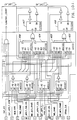
control state machine 200, shown in Figure 8. Thecontrol state machine 200 includes a first program logic array (PLA0) 300 and a second program logic array (PLA1) 301, which provide combinatorial logic for combining the various input signals to thecontrol state machine 200 to provide logic output signals. The DRAM clock at the terminal 204 clocks a number of D flip flops to latch the combinatorial outputs of theprogram logic arrays - Figure 10 shows the circuit details for the
address generator 202 shown in Figure 8. Essentially, these circuits implement the connection arrangement of Table 2. The internal address signals provided on thebus 236 are distributed on that bus to various and/or/invert stages, which function asmultiplexers 401 to 409 for selection of these address lines in accordance with the internal logic provided by thecontrol state machine 200 and various other logic elements as shown in Figure 10A and 10B. Each of thesemultiplexers 401 to 409 has its output signal coupled to the D input terminals of a respectiveD flip flop 410 to 418, which latch the output signals of these multiplexers under control of the DRAM clock provided at the terminal 204. The various column count signals CNTN as indicated in Table 2 are provided by output signals from certain of theD flip flops 413 to 418 being coupled throughmultiplexers 420 to 425 and latched into the inputs of theD flip flops 413 to 418. - Note that all of the logic elements shown in the drawings are standard cells and building blocks provided by the ATNT 1.25 micron CMOS cell library.
Claims (14)
- A method for temporarily storing and retrieving q-bit character information data for an information storage system in a y-bit wide buffer memory unit comprising a plurality of DRAMS, with q being greater than y, characterised by:providing a virtual memory address for each item of q-bit character information data, said character information data being organised into a block comprising z said information characters;translating the virtual memory addresses into corresponding addresses of memory locations in said buffer memory unit for storage of y-bit groups of said block in said buffer memory unit, said translating step includingselecting a row address for storage of said block,selecting a base column address for said block, andsuccessively incrementing said base column address to provide additional column addresses for successive y-bit groups of said block;transferring each of said y-bit groups of said block via a y-bit data bus to an address location in said buffer memory unit determined by said translating step;providing a x-bit error detection code word for each said block;selecting an address for storing said x-bit error detection code word in said buffer memory unit; said selecting an address including:selecting an error detection code word row address;selecting an error detection code word base column address for a first y-bit group of said x-bit error detection code word;incrementing said error detection code word base column address by y to provide a second column address for a second y-bit group of said x-bit error detection code word; andtransferring said error detection code word via said y-bit data bus to the selected address locations for said x-bit error detection code word in said buffer memory unit.
- A memory as claimed in claim 1, in which said error detection code words are stored in a first substantially contiguous address space in said buffer memory unit, and said character information data items are stored in a second substantially contiguous address space in said buffer memory unit separate from said first address space, said error detection code words being stored separately from the character information data to which they pertain.
- A method as claimed in either claim 1 or 2, in which translating the virtual memory address includes selecting the row and column address using multiplexer circuits.
- A method as claimed in any one of claims 1 to 3, further comprising latching the row and column addresses into latch circuits, and wherein successively incrementing said base column address includes coupling outputs from the latch circuits via multiplexing circuits coupled to the inputs of the latch circuits.
- A method as claimed in any one of claims 1 to 4, in which the buffer memory unit comprises a DRAM operating in a page mode.
- A method as claimed in any one of claims 1 to 4, in which the buffer memory unit comprises a DRAM operating in a static column mode.
- A method as claimed in any one of claims 1 to 6, in which transferring said error detection code word includes forming an address for each provided said error detection code word from said base address of said block of data by right-shifting said base address of said block of data by a pre-determined number of bits and filling the thus-vacated upper bit positions with a fixed bit pattern.
- A method as claimed in any one of the preceding claims, in which q is 8, x is 8, y is 4 and z is 16.
- A method as claimed in any one of the preceding claims, in which said information storage system includes a magnetic disk.
- A method for temporarily storing and retrieving q-bit character information data for an information storage system in a y-bit wide buffer memory unit comprising a plurality of DRAMS, with q being greater than y, characterised by:providing a virtual memory address for each item of q-bit character information data, said character information data being organised into a block comprising z said information characters;translating the virtual memory addresses into corresponding addresses of memory locations in said buffer memory unit for storage of y-bit groups of said block in said buffer memory unit, said translating step includingselecting a row address for storage of said block,selecting a base column address for said block,latching said row and base column addresses into latch circuits, andsuccessively incrementing said base column address to provide additional column addresses for successive y-bit groups of said block by coupling outputs of said latch circuits via multiplexing circuits coupled to inputs of said latch circuits to increment said column addresses; andtransferring each of said y-bit groups of said block via a y-bit data bus to an address location in said buffer memory unit determined by said translating step.
- A method as claimed in claim 10, further comprising:providing a x-bit error detection code word for each said block;selecting an address for storing said x-bit error detection code word in said buffer memory unit; said selecting an address including:selecting an error detection code word row address;selecting an error detection code word base column address for a first y-bit group of said x-bit error detection code word;incrementing said error detection code word base column address by y to provide a second column address for a second y-bit group of said x-bit error detection code word; andtransferring said error detection code word via said y-bit data bus to the selected address locations for said x-bit error detection code word in said buffer memory unit.
- A method as claimed in any one of the preceding claims, in which successively incrementing said base column address to provide additional column addresses for successive y-bit groups of said block comprises successively incrementing said base column address by y to provide additional column addresses for successive y-bit groups of said block.
- A method as claimed in any one of claims 10, 11 and 12 when dependent upon claim 11, in which selecting an error detection code word row address comprises: selecting an error detection code word row address different from said row address selected for storage of said block; and selecting an error detection code word comprises selecting an error detection code word base column address for a first y-bit group of said x-bit error detection code word different from said selected block base column address; said character information being stored substantially contiguously in said buffer memory unit; and said error detection code words being stored substantially contiguously in said buffer memory unit and separate from said character information data to which said error detection code words pertain.
- A method as claimed in any one of claims 1 to 13, in which said q-bit character information consists of 8-bit character information data, said character information being organised into 16-byte blocks, said y-bit wide buffer memory consists of 4-bit wide DRAM, and said x-bit error detection code word consists of an 8-bit code word.
Applications Claiming Priority (2)
| Application Number | Priority Date | Filing Date | Title |
|---|---|---|---|
| US07/487,740 US5280601A (en) | 1990-03-02 | 1990-03-02 | Buffer memory control system for a magnetic disc controller |
| US487740 | 1990-03-02 |
Publications (3)
| Publication Number | Publication Date |
|---|---|
| EP0444885A2 EP0444885A2 (en) | 1991-09-04 |
| EP0444885A3 EP0444885A3 (en) | 1995-01-25 |
| EP0444885B1 true EP0444885B1 (en) | 1999-05-06 |
Family
ID=23936929
Family Applications (1)
| Application Number | Title | Priority Date | Filing Date |
|---|---|---|---|
| EP91301553A Expired - Lifetime EP0444885B1 (en) | 1990-03-02 | 1991-02-26 | A method for controlling a buffer memory for a magnetic disk storage system |
Country Status (5)
| Country | Link |
|---|---|
| US (1) | US5280601A (en) |
| EP (1) | EP0444885B1 (en) |
| JP (1) | JP2772150B2 (en) |
| DE (1) | DE69131186T2 (en) |
| SG (1) | SG47724A1 (en) |
Families Citing this family (22)
| Publication number | Priority date | Publication date | Assignee | Title |
|---|---|---|---|---|
| US5655147A (en) * | 1991-02-28 | 1997-08-05 | Adaptec, Inc. | SCSI host adapter integrated circuit utilizing a sequencer circuit to control at least one non-data SCSI phase without use of any processor |
| IL100127A0 (en) * | 1991-03-11 | 1992-08-18 | Future Domain Corp | Scsi controller |
| US5371861A (en) * | 1992-09-15 | 1994-12-06 | International Business Machines Corp. | Personal computer with small computer system interface (SCSI) data flow storage controller capable of storing and processing multiple command descriptions ("threads") |
| US5537425A (en) * | 1992-09-29 | 1996-07-16 | International Business Machines Corporation | Parity-based error detection in a memory controller |
| US5659690A (en) * | 1992-10-15 | 1997-08-19 | Adaptec, Inc. | Programmably configurable host adapter integrated circuit including a RISC processor |
| US5379261A (en) * | 1993-03-26 | 1995-01-03 | United Memories, Inc. | Method and circuit for improved timing and noise margin in a DRAM |
| KR0139776B1 (en) * | 1993-11-26 | 1998-07-15 | 이헌조 | Dram controlling apparatus of cd graphics decorder |
| AU1303595A (en) * | 1993-12-14 | 1995-07-03 | Apple Computer, Inc. | Method and apparatus for transferring data between a computer and a peripheral storage device |
| US5983309A (en) * | 1994-07-27 | 1999-11-09 | Seagate Technology, Inc. | Autonomous high speed address translation with defect management for hard disc drives |
| US5729719A (en) * | 1994-09-07 | 1998-03-17 | Adaptec, Inc. | Synchronization circuit for clocked signals of similar frequencies |
| WO1996032674A2 (en) * | 1995-04-13 | 1996-10-17 | Cirrus Logic, Inc. | Semiconductor memory device for mass storage block access applications |
| US5692165A (en) * | 1995-09-12 | 1997-11-25 | Micron Electronics Inc. | Memory controller with low skew control signal |
| US5765203A (en) * | 1995-12-19 | 1998-06-09 | Seagate Technology, Inc. | Storage and addressing method for a buffer memory control system for accessing user and error imformation |
| US6021482A (en) * | 1997-07-22 | 2000-02-01 | Seagate Technology, Inc. | Extended page mode with a skipped logical addressing for an embedded longitudinal redundancy check scheme |
| US6148388A (en) * | 1997-07-22 | 2000-11-14 | Seagate Technology, Inc. | Extended page mode with memory address translation using a linear shift register |
| US6009547A (en) * | 1997-12-03 | 1999-12-28 | International Business Machines Corporation | ECC in memory arrays having subsequent insertion of content |
| US6925589B1 (en) * | 1998-10-29 | 2005-08-02 | International Business Machines Corporation | Method for translating physical cell-coordinates of a memory product to n-dimensional addresses |
| JP3778540B2 (en) * | 1999-05-17 | 2006-05-24 | 東芝デジタルメディアエンジニアリング株式会社 | Signal processing circuit and information recording apparatus |
| JP2002170399A (en) * | 2000-12-05 | 2002-06-14 | Fujitsu Ltd | Semiconductor device |
| US20040268033A1 (en) * | 2003-06-24 | 2004-12-30 | Seagate Technology Llc | Refreshing data in a data storage device |
| US7836380B2 (en) * | 2006-10-31 | 2010-11-16 | Intel Corporation | Destination indication to aid in posted write buffer loading |
| US7961532B2 (en) * | 2008-06-27 | 2011-06-14 | Rambus Inc. | Bimodal memory controller |
Citations (1)
| Publication number | Priority date | Publication date | Assignee | Title |
|---|---|---|---|---|
| EP0226950A2 (en) * | 1985-12-23 | 1987-07-01 | Kabushiki Kaisha Toshiba | Memory access control circuit |
Family Cites Families (17)
| Publication number | Priority date | Publication date | Assignee | Title |
|---|---|---|---|---|
| GB2112256B (en) * | 1981-11-18 | 1985-11-06 | Texas Instruments Ltd | Memory apparatus |
| US4514806A (en) * | 1982-09-30 | 1985-04-30 | Honeywell Information Systems Inc. | High speed link controller wraparound test logic |
| US4683555A (en) * | 1985-01-22 | 1987-07-28 | Texas Instruments Incorporated | Serial accessed semiconductor memory with reconfigureable shift registers |
| US4916603A (en) * | 1985-03-18 | 1990-04-10 | Wang Labortatories, Inc. | Distributed reference and change table for a virtual memory system |
| US4819152A (en) * | 1985-04-05 | 1989-04-04 | Raytheon Company | Method and apparatus for addressing a memory by array transformations |
| US4672613A (en) * | 1985-11-01 | 1987-06-09 | Cipher Data Products, Inc. | System for transferring digital data between a host device and a recording medium |
| US4803621A (en) * | 1986-07-24 | 1989-02-07 | Sun Microsystems, Inc. | Memory access system |
| US4845664A (en) * | 1986-09-15 | 1989-07-04 | International Business Machines Corp. | On-chip bit reordering structure |
| JPS63186345A (en) * | 1987-01-29 | 1988-08-01 | Toshiba Corp | Address multiplexing control circuit |
| US5007020A (en) * | 1987-03-18 | 1991-04-09 | Hayes Microcomputer Products, Inc. | Method for memory addressing and control with reversal of higher and lower address |
| US5057837A (en) * | 1987-04-20 | 1991-10-15 | Digital Equipment Corporation | Instruction storage method with a compressed format using a mask word |
| DE3786080D1 (en) * | 1987-08-20 | 1993-07-08 | Ibm | MEMORY ACCESS CONTROL DEVICE IN A MIXED DATA FORMAT SYSTEM. |
| US4992956A (en) * | 1987-10-08 | 1991-02-12 | Advanced Micro Devices, Inc. | Apparatus for assembling data for supply to a scanning output device |
| US4888773A (en) * | 1988-06-15 | 1989-12-19 | International Business Machines Corporation | Smart memory card architecture and interface |
| US4916654A (en) * | 1988-09-06 | 1990-04-10 | International Business Machines Corporation | Method for transfer of data via a window buffer from a bit-planar memory to a selected position in a target memory |
| US5058005A (en) * | 1988-09-09 | 1991-10-15 | Compaq Computer Corporation | Computer system with high speed data transfer capabilities |
| US5065312A (en) * | 1989-08-01 | 1991-11-12 | Digital Equipment Corporation | Method of converting unique data to system data |
-
1990
- 1990-03-02 US US07/487,740 patent/US5280601A/en not_active Expired - Fee Related
-
1991
- 1991-02-26 EP EP91301553A patent/EP0444885B1/en not_active Expired - Lifetime
- 1991-02-26 SG SG1996004071A patent/SG47724A1/en unknown
- 1991-02-26 DE DE69131186T patent/DE69131186T2/en not_active Expired - Fee Related
- 1991-03-01 JP JP3036291A patent/JP2772150B2/en not_active Expired - Fee Related
Patent Citations (1)
| Publication number | Priority date | Publication date | Assignee | Title |
|---|---|---|---|---|
| EP0226950A2 (en) * | 1985-12-23 | 1987-07-01 | Kabushiki Kaisha Toshiba | Memory access control circuit |
Also Published As
| Publication number | Publication date |
|---|---|
| JPH06131124A (en) | 1994-05-13 |
| HK1013344A1 (en) | 1999-08-20 |
| DE69131186T2 (en) | 1999-08-26 |
| SG47724A1 (en) | 1998-04-17 |
| US5280601A (en) | 1994-01-18 |
| EP0444885A3 (en) | 1995-01-25 |
| DE69131186D1 (en) | 1999-06-10 |
| JP2772150B2 (en) | 1998-07-02 |
| EP0444885A2 (en) | 1991-09-04 |
Similar Documents
| Publication | Publication Date | Title |
|---|---|---|
| EP0444885B1 (en) | A method for controlling a buffer memory for a magnetic disk storage system | |
| US5394541A (en) | Programmable memory timing method and apparatus for programmably generating generic and then type specific memory timing signals | |
| US6125072A (en) | Method and apparatus for contiguously addressing a memory system having vertically expanded multiple memory arrays | |
| US7783957B2 (en) | Apparatus for implementing enhanced vertical ECC storage in a dynamic random access memory | |
| EP0410566B1 (en) | Data processing system with means to convert burst operations into pipelined operations | |
| EP0646928A2 (en) | Synchronous dynamic random access memory | |
| US5765203A (en) | Storage and addressing method for a buffer memory control system for accessing user and error imformation | |
| CN100419901C (en) | Memory device with different burst sequential addressing for read and write operations | |
| US7340584B2 (en) | Sequential nibble burst ordering for data | |
| US5630054A (en) | Method and apparatus for storing and retrieving error check information | |
| US5343425A (en) | Semiconductor video memory having multi-ports | |
| US4796222A (en) | Memory structure for nonsequential storage of block bytes in multi-bit chips | |
| JPS5837883A (en) | Memory addressing unit | |
| TW491970B (en) | Page collector for improving performance of a memory | |
| US4992979A (en) | Memory structure for nonsequential storage of block bytes in multi bit chips | |
| EP0327115A1 (en) | Serial access memory system provided with improved cascade buffer circuit | |
| US7191295B2 (en) | Sensing word groups in a memory | |
| HK1013344B (en) | A method for controlling a buffer memory for a magnetic disk storage system | |
| US7191305B2 (en) | Method and apparatus for address decoding of embedded DRAM devices | |
| EP1067555B1 (en) | Memory controller and an information processing apparatus having such a memory controller | |
| JPS6180447A (en) | Storage device store control method | |
| JPH02195457A (en) | Error detector of semiconductor memory device | |
| JPS60108941A (en) | Memory interface circuit | |
| JPS5831459A (en) | Magnetic bubble memory device |
Legal Events
| Date | Code | Title | Description |
|---|---|---|---|
| PUAI | Public reference made under article 153(3) epc to a published international application that has entered the european phase |
Free format text: ORIGINAL CODE: 0009012 |
|
| AK | Designated contracting states |
Kind code of ref document: A2 Designated state(s): DE FR GB IT NL |
|
| PUAL | Search report despatched |
Free format text: ORIGINAL CODE: 0009013 |
|
| AK | Designated contracting states |
Kind code of ref document: A3 Designated state(s): DE FR GB IT NL |
|
| 17P | Request for examination filed |
Effective date: 19950718 |
|
| 17Q | First examination report despatched |
Effective date: 19960926 |
|
| GRAG | Despatch of communication of intention to grant |
Free format text: ORIGINAL CODE: EPIDOS AGRA |
|
| GRAG | Despatch of communication of intention to grant |
Free format text: ORIGINAL CODE: EPIDOS AGRA |
|
| GRAH | Despatch of communication of intention to grant a patent |
Free format text: ORIGINAL CODE: EPIDOS IGRA |
|
| GRAH | Despatch of communication of intention to grant a patent |
Free format text: ORIGINAL CODE: EPIDOS IGRA |
|
| GRAA | (expected) grant |
Free format text: ORIGINAL CODE: 0009210 |
|
| AK | Designated contracting states |
Kind code of ref document: B1 Designated state(s): DE FR GB IT NL |
|
| PG25 | Lapsed in a contracting state [announced via postgrant information from national office to epo] |
Ref country code: IT Free format text: LAPSE BECAUSE OF FAILURE TO SUBMIT A TRANSLATION OF THE DESCRIPTION OR TO PAY THE FEE WITHIN THE PRESCRIBED TIME-LIMIT;WARNING: LAPSES OF ITALIAN PATENTS WITH EFFECTIVE DATE BEFORE 2007 MAY HAVE OCCURRED AT ANY TIME BEFORE 2007. THE CORRECT EFFECTIVE DATE MAY BE DIFFERENT FROM THE ONE RECORDED. Effective date: 19990506 Ref country code: FR Free format text: LAPSE BECAUSE OF FAILURE TO SUBMIT A TRANSLATION OF THE DESCRIPTION OR TO PAY THE FEE WITHIN THE PRESCRIBED TIME-LIMIT Effective date: 19990506 Ref country code: NL Free format text: LAPSE BECAUSE OF FAILURE TO SUBMIT A TRANSLATION OF THE DESCRIPTION OR TO PAY THE FEE WITHIN THE PRESCRIBED TIME-LIMIT Effective date: 19990506 |
|
| REF | Corresponds to: |
Ref document number: 69131186 Country of ref document: DE Date of ref document: 19990610 |
|
| EN | Fr: translation not filed | ||
| PGFP | Annual fee paid to national office [announced via postgrant information from national office to epo] |
Ref country code: GB Payment date: 20000124 Year of fee payment: 10 |
|
| PGFP | Annual fee paid to national office [announced via postgrant information from national office to epo] |
Ref country code: DE Payment date: 20000131 Year of fee payment: 10 |
|
| PLBE | No opposition filed within time limit |
Free format text: ORIGINAL CODE: 0009261 |
|
| STAA | Information on the status of an ep patent application or granted ep patent |
Free format text: STATUS: NO OPPOSITION FILED WITHIN TIME LIMIT |
|
| 26N | No opposition filed | ||
| PG25 | Lapsed in a contracting state [announced via postgrant information from national office to epo] |
Ref country code: GB Free format text: LAPSE BECAUSE OF NON-PAYMENT OF DUE FEES Effective date: 20010226 |
|
| GBPC | Gb: european patent ceased through non-payment of renewal fee |
Effective date: 20010226 |
|
| PG25 | Lapsed in a contracting state [announced via postgrant information from national office to epo] |
Ref country code: DE Free format text: LAPSE BECAUSE OF NON-PAYMENT OF DUE FEES Effective date: 20011201 |