EP0444794A2 - Diagnostic system for textile dyeing apparatus - Google Patents
Diagnostic system for textile dyeing apparatus Download PDFInfo
- Publication number
- EP0444794A2 EP0444794A2 EP91301122A EP91301122A EP0444794A2 EP 0444794 A2 EP0444794 A2 EP 0444794A2 EP 91301122 A EP91301122 A EP 91301122A EP 91301122 A EP91301122 A EP 91301122A EP 0444794 A2 EP0444794 A2 EP 0444794A2
- Authority
- EP
- European Patent Office
- Prior art keywords
- look
- data
- pattern
- tables
- control system
- Prior art date
- Legal status (The legal status is an assumption and is not a legal conclusion. Google has not performed a legal analysis and makes no representation as to the accuracy of the status listed.)
- Granted
Links
Images


Classifications
-
- G—PHYSICS
- G06—COMPUTING; CALCULATING OR COUNTING
- G06F—ELECTRIC DIGITAL DATA PROCESSING
- G06F11/00—Error detection; Error correction; Monitoring
- G06F11/22—Detection or location of defective computer hardware by testing during standby operation or during idle time, e.g. start-up testing
-
- D—TEXTILES; PAPER
- D06—TREATMENT OF TEXTILES OR THE LIKE; LAUNDERING; FLEXIBLE MATERIALS NOT OTHERWISE PROVIDED FOR
- D06B—TREATING TEXTILE MATERIALS USING LIQUIDS, GASES OR VAPOURS
- D06B11/00—Treatment of selected parts of textile materials, e.g. partial dyeing
- D06B11/0056—Treatment of selected parts of textile materials, e.g. partial dyeing of fabrics
- D06B11/0059—Treatment of selected parts of textile materials, e.g. partial dyeing of fabrics by spraying
Abstract
Description
- This invention relates to a textile dyeing apparatus and, more particularly, to a diagnostic system for the textile dyeing apparatus which detects and isolates errors in the apparatus control system.
- A known modern textile dyeing apparatus includes multiple arrays or color bars, each comprising a plurality of individual, electronically addressable dye jets. Each of the dye jets in a single array outputs the same color of dye. The arrays are positioned in spaced relation across the path of a moving substrate.
- Using such apparatus, the pattern-wise application of dye to the textile materials or substrates requires a large quantity of digitally encoded pattern data which must be sorted and routed to each of the individual dye jets comprising each of the arrays. Each of the arrays of dye jets extends across the width of the substrate path as the substrate moves under the arrays. The time period during which the dye streams produced by the individual dye jets in a given array are allowed to strike the substrate are individually controlled. This allows for shade variations to be produced from side-to-side (and end-to-end) on the substrate by varying the quantity of dye applied to the substrate along the length of a given array.
- One such control system capable of providing this capability is described in co-pending U.S. Serial Number 327,843, entitled "DATA LOADING AND DISTRIBUTING PROCESS AND APPARATUS FOR CONTROL OF A PATTERNING PROCESS", filed on March 23, 1989, the specification of which is hereby incorporated by reference. This system processes pattern data received from a real-time processor through the use of specific electronic circuitry which accepts the pattern data in the form of a series of 8-bit units. Each of the 8-bit units or pixel codes uniquely identifies, for each pattern element or pixel, a pattern design element to be associated with that pattern element or pixel.
- The term "pattern element" as used herein is intended to be analogous to the term "pixel" as that term is used in the field of electronic imaging. The number of different pattern design elements is equal to the number of distinct areas of the pattern which may be assigned a separate color.
- The term "pattern line" as used herein is intended to describe a continuous line of single pattern elements extending across the substrate, parallel to the patterning arrays. Such pattern lines have a thickness, measured in the direction of substrate travel, equal to the maximum permitted amount of substrate travel under the patterning arrays between array pattern data updates.
- In this control system, the pixel codes must first be converted to "on/off" firing instructions, (referring to the actuation or deactuation, respectively, of the individual dye streams produced by the dye jets). This is performed by electronically associating the "raw" pixel codes with pre-generated firing instruction data from a computer generated look-up table. The pixel codes merely define those distinct areas of the pattern which may be assigned a distinguishing color. Each code specifies, for each pattern line, the dye jet response for a given dye jet position on each and every array. In this system the number of arrays equal eight; therefore, each pixel code controls the response of eight separate dye jets (one per array) with respect to a single pattern line.
- The pixel codes for a given array is preferably arranged in sequence, with data for dye jets 1-N for the first pattern line being first in he series, followed by data for dye jets 1-N for the second pattern line, etc. The complete serial stream of such pixel codes is sent to a firing time converter and memory associated with each respective array for conversion of the pixel codes into the respective firing times.
- Each firing time converter includes a look-up table having a sufficient number of addresses so that each possible address code forming the serial stream of pattern data may be assigned a unique address in the look-up table. At each address within the look-up table is a byte representing a relative firing time or dye contact time, which, assuming an 8-bit value at the address code of interest, can be zero or one of 255 different discreet time values corresponding to the relative amount of time the dye jet in question is to remain "on". Therefore, each specific dye jet location on each and every array can be assigned one of 256 different firing times.
- The firing time data from the look-up table for each array is then further processed to account for the "stagger", e.g., the physical spacing between arrays, and the allocation of the individual firing instructions for each jet in the array. The process of sequencing the individual pattern line data to accommodate substrate travel time or stagger between adjacent arrays is performed through the use of array-specific Random Access Memories (RAMs), which are preferably of the static type. All pattern data for a specific array is loaded into a RAM individually associated with that array. The pattern data is in the form of a series of bytes, each byte specifying a desired firing time for a single applicator or jet comprising the array. The loading process is a coordinated one, with all jet firing time data being loaded into the respective RAMs at the same time and in the same relative order, i.e., all firing times corresponding to the first line of the pattern for all jets in each array is loaded in the appropriate RAM first, followed by all data corresponding to the second pattern line, etc. Each RAM is read using reading address offsets which effectively delay the reading of the data a sufficient amount of time to allow a specific area of the substrate to "catch up" to the corresponding pattern data for that specific area which will be sent to the next array along the substrate path.
- At this time, the series of individual firing times expressed in byte form are transferred into a sequence of individual binary digit ("bit") groups. Each group in the sequence represents the value of its corresponding respective firing time by the relative number of binary digits of a predetermined logic value (e.g., logical "one" = "fire") which are sequentially "stacked" within each group. This transformation allows the firing times, expressed in byte form, to be expressed as a continuing sequence of individual firing commands (i.e., single bits) which may be recognized by the applicators.
- Finally, the individual firing instructions for each jet in the array are loaded into a collection of First-In First-Out Memories (FIFOs). Each array is associated with an individual set of FIFOs. Each FIFO repeatedly sends its contents, one byte at a time and strictly in the order in which the bytes were originally loaded, to a comparator.
- The value of the byte, representing a desired elapsed firing time of a single jet along the array, is compared with a clock value which has been initialized to provide a value representing the smallest increment of time for which control of any jet is desired. As a result of the comparison, a firing command in the form of a logical "one" or logical "zero", which signifies that the jet is to "fire" or "not fire", respectively, is generated and is forwarded to a shift register associated with the array, as well as to a detector. After all bytes (representing all jet locations along that array) have been sent and compared, the contents of the shift register are forwarded, in parallel, to the air valve assemblies along the array by way of a latch associated with the shift register. Thereafter, the counter value is incremented, the same contents of the FIFO are compared with the new counter value, and the contents of the shift register are again forwarded, in a parallel format and via a latch, to the air valve assemblies in the array.
- At some counter value, all elapsed firing times read from the FIFOs will be less than or equal to that value of the counter. When this condition exists at every array, fresh data, representing a new pattern line, is forwarded from the RAM in response to a transducer pulse indicating the substrate has moved an amount equivalent to one pattern line. This fresh data is loaded into the FIFOs and a new series of iterative comparisons is initiated, using a re-initialized counter. This process is repeated until all pattern lines have been processed. If the pattern is to be repeated, the RAM re-initiates the above procedure by sending the first pattern line to the appropriate FIFO's.
- The known control system thus includes a large number of hardware components, i.e., look-up tables, stagger memories, and FIFOs associated with each color bar in the apparatus, all of which must operate properly to insure that the source pattern data is correctly transformed and printed on the substrate. There is therefore needed a diagnostic system which can check the major components in the control system to determine whether it is operating properly. Because of the extremely large number of components to be checked, the diagnostic system must be able to operate quickly and efficiently.
- The present invention provides an efficient diagnostic system capable of checking the major hardware components in the pattern control system such as the look-up tables, stagger memories, and FIFOs associated with each color bar in the apparatus.
- The diagnostic system includes bypass logic circuitry which permits selective bypassing of either the look-up tables, stagger memory, or both the look-up tables and the stagger memories in the pattern control system. This allows test patterns provided by the diagnostic system to selectively bypass certain of the control system components to isolate the occurrence of any errors detected. Bypass lines around each component are fed to logic circuitry performing "OR" operation to enable either the bypassed data or normal data to pass through the logic to the rest of the system. The same logic circuitry is utilized with respect to each of the components. The enable signals are received from a register which is loaded in accordance with the diagnostic performed.
- It is an advantage of the bypass circuitry to allow the isolation of any component from the rest of the system. Further, test pattern data can be provided directly to the gatling memory thus avoiding time delays inherent with the operation of the stagger memory. In normal day to day production operation, the bypass logic allows the checking of dye jets and flows without having to wait for the stagger memory to compensate for downstream color bars.
- The present invention further provides for a diagnostic check of the look-up tables in the pattern control system. The diagnostic assures that the address lines for the look-up tables operate properly, i.e., the address lines are capable of correctly specifying each unique address within each single look-up table among a group of look-up tables. The look-up tables are loaded with a "prime number pattern" which is repeated to fill up each of the look-up tables for each of the color bars. A "count pattern" of addresses is then input to the look-up table from which a respective sequence of the prime number pattern is output. The output from the look-up tables is then compared with an identical copy of the prime number pattern to determine the coincidence of each pattern.
- It is an advantage of the present invention to use a prime number pattern to load the look-up tables such that each address location for each look-up table will have a different piece of data. This ensures that any address lines causing incorrect addressing can be determined.
- The present invention also provides for a diagnostic check of the firing times produced by the gatling memory section of the pattern control system. The diagnostic system simulates a machine speed-up, and then checks for the onset of machine "optimum speed" and machine "overspeed". These two machine conditions indicate whether the speed of the substrate traveling under the dye jets is approaching, or has exceeded, respectively, the maximum speed at which the individual valves controlling the application of dye on the substrate can operate. The detection of these machine conditions provides signals to the system such that the diagnostic is made aware of these conditions as they occur.
- It is an advantage of the firing time diagnostic to assure that all of the hardware is operating properly.
- Details of the present invention herein, as well as additional advantages and distinguishing features, will be better understood with reference to the following figures.
-
- Figure 1 is a block diagram illustrating one pattern control system environment in which the present invention may operate;
- Figure 2 is a diagramatic side elevation view of a jet dyeing apparatus to which the present invention is particularly well adapted;
- Figure 3 is a schematic side elevation view of the apparatus of Figure 2, showing only a single dye jet color bar and its operative connection to a liquid dye system as well as several electronic subsystems associated with the apparatus;
- Figure 4 is a schematic block diagram illustrating in greater detail the real-time computer and pattern control system of Figure 1;
- Figure 5 is a block diagram further disclosing the control system of the apparatus;
- Figures 6A and 6B are diagramatic representations of the "stagger" memory disclosed in Figure 5. Figure 6A depicts a memory state at a time T1; Figure 6B depicts a memory state at time T2, exactly 100 pattern lines later;
- Figure 7 is block diagram describing the "gatling" memory described in Figure 5;
- Figure 8 schematically depicts the format of the pattern data at various data processing stages as indicated in Figures 5-7;
- Figure 9 is a schematic block diagram illustrating the diagnostic bypass logic;
- Figure 10 is a block diagram of the look-up tables in Figure 4, illustrating the operation of the LUT diagnostic;
- Figure 11 is a block diagram of the FIFO register in the gatling memory section in Figures 4 and 5;
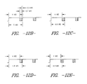
- Figures 12A-12E are timing diagrams illustrating the operation of the FIFO diagnostic.
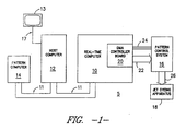
- Referring to Figure 1, a
multiprocessor patterning system 5 is shown having ahost computer 12 coupled via abus 11 to a real-time computer 10.Optional pattern computer 14 is further coupled to thehost computer 12 and real-time computer 10 by thebus 11. It is readily apparent that the coupling of thepattern computer 14,host computer 12 and real-time computer 10 may be by any means for coupling a local area network (LAN) such as an Ethernet bus. - A
pattern control system 16 is coupled viabus 26 to ajet dyeing apparatus 18. Thejet dyeing apparatus 18 is described in greater detail in Figures 2 and 3. Thepattern control system 16 receives inputs frombus 22 and channelselect lines 24 of the programmableDMA controller board 20. The programmableDMA controller board 20 is part of the real-time computer 10 and is described in greater detail in Figure 2. -
Optional pattern computer 14 may be provided to allow a user of the system to quickly create their own pattern design. Alternatively, pattern designs may be pre-loaded onto magnetic or optical media (not shown) for reading into the system. Acomputer terminal 13 may be coupled via asuitable connection 17, e.g., a standard RS232 cable, to thehost computer 12. The terminal 13 then serves as the operator's interface for providing the input parameters to the host computer for each "job" of patterns to be generated on the substrate byjet dyeing apparatus 18. Thehost computer 12 also fetches the pattern data from he pattern computer or other source and sets it up for processing by the real-time computer 10. The real-time computer 10 functions to insure that the pattern data is properly output to thepattern control system 16 by programming appropriately theDMA controller board 20. - Figure 2 shows a
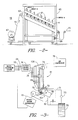
jet dyeing apparatus 18 comprised of a set of eightindividual color bars 61 positioned withinframe 65. Eachcolor bar 61 is comprised of a plurality of dye jets, perhaps several hundred in number, arranged in spaced alignment along the length of the color bar, which color bar extends across the width ofsubstrate 15.Substrate 15, such as a textile fabric, is supplied fromroll 67 as transported throughframe 65 and thereby under eachcolor bar 61 byconveyor 63 driven by a motor indicated generally at 69. After being transported undercolor bars 61,substrate 15 may be passed through other dyeing-related color steps such as drying, fixing, etc. - Referring to Figure 3, there is shown in schematic form a side elevation of one
color bar 61 comprising thejet dyeing apparatus 18 of Figure 2. For eachsuch color bar 61, a separatedye reservoir tank 75 supplies liquid dye under pressure by means ofpump 73 and dye supply conduit means 71, to a primarydye manifold assembly 70 of thecolor bar 61.Primary manifold assembly 70 communicates with and supplies dye to dyesub-manifold assembly 41 at suitable locations along their respective lengths. Bothmanifold assembly 70 andsub-manifold assembly 41 extend across the width ofconveyor 63 on which the substrate to be dyed is transported.Sub-manifold assembly 41 is provided with a plurality of spaced, generally downwardly directed dye passage outlets positioned across the width ofconveyor 63 which produce a plurality of parallel dye streams which are directed onto the substrate surface to be patterned. - Positioned in alignment with and approximately perpendicular to each dye passage outlet (not shown) in
sub-manifold assembly 41 is the outlet of an air deflection tube 62. Each tube 62 communicates by way of anair deflection conduit 64 with an individual electro-pneumatic valve, illustrated collectively at "V", which valve selectively interrupts the flow of air to air tube 62 in accordance with the pattern information supplied bypattern control system 16. Each valve is, in turn, connected by an air supply conduit to a pressurizedair supply manifold 74 which is provided with pressurized air byair compressor 76. Each of the valves V, which may be, for example, of the electromagnetic solenoid type, are individually controlled by electrical signals received overbus 26 from the electronicpattern control system 16. The outlets of deflection tubes 62 direct streams of air which are aligned with and impinge against the continuously flowing streams of dye flowing from downwardly directed dye passages withinsub-manifold 41 and deflect such streams into a primary collection chamber ortrough 80, from which liquid dye is removed, by means of a suitabledye collection conduit 82, to dyereservoir tank 75 for recirculation. - The
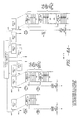
pattern control system 16 receives pattern data overbus 22 and control information overlines 24 from the multiprocessor system described in Figure 1. The desired pattern information fromcontrol system 16 is transmitted to the solenoid valves of eachcolor bar 61 at appropriate times in response to movement of the substrate under the color bars byconveyor 63, which movement is detected by a suitable rotary motion sensor or transducer means 19 operatively associated with theconveyor 63 and connected to controlsystem 16. - Referring to Figure 4, the real-
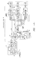
time computer 10 is shown havingmemory 34 and programmableDMA controller board 20. Pattern data is received from thehost computer 12 via thebus 11 and stored onhigh speed disk 33 by way of diagrammatically depictedlinks high speed disk 33 intomemory 34, vialink 35, for access byDMA controller 20 viabus 36. - The programmable
DMA controller board 20 is shown comprising aprogrammable DMA processor 32,FIFO buffer 28 and 3-bit latch 30. Theprogrammable DMA processor 32 couples withbus 36 vialine 38 and withFIFO buffer 28 vialine 37. Further, the 3-bit latch 30 is coupled to thebus 36 vialine 39. It should be understood that Figure 4 shows only a simplified diagrammatically depicted version of the programmableDMA controller board 20. A more complete and accurate description of thecontroller board 20 can be found by consulting the specifications thereof; for example, thecontroller board 20 may be of the type produced by Digital Equipment Corporation as Model DRQ3B or may be the Intel 82258 DMA chip used in conjunction with a host computer card such as the Intel 286/12 Board. - Pattern numbers chosen by the
operator using terminal 13 are entered vialine 17, into host computer 12 (Figure 1).Computer 12 loads pattern data from, e.g.,pattern computer 14, ontohigh speed disk 33, and then sends data messages to real-time computer 10.Computer 10, on receipt of such messages, loads the requested pattern data fromhigh speed disk 33 intomemory 34. When requested by means of an interrupt, as by the occurrence of a transducer pulse indicating a predetermined length of substrate has passed under the patterning jets, the real-time computer 10 commands theDMA controller 20 to initiate the transfer of the appropriate pattern data stored inmemory 34 to thepattern control system 16, viaFIFO buffer 28. - A first-in-first-out (FIFO)
buffer 28 stores words (16-bits) of pattern data in each buffer location. The pattern data stored inFIFO buffer 28 is then output to thepattern control system 16 along the high-speed (e.g., 2.6 megabytes/second)data bus 22. TheFIFO buffer 28 serves as an interface between the rate at which data is placed into theFIFO buffer 28 byDMA processor 32 and the rate at which data is output to thepattern control system 16. If thepattern control system 16 operates at a rate equal to or greater than that of the real-time processor 10,FIFO buffer 28 would not be needed to perform such interface function. - The
DMA processor 32 also functions to requestmemory 34 to provide inputs vialine 39 to the 3-bit latch 30 as real-time computer 10 commands it to do so. Thelatch 30 provides a parallel output on the three channelselect lines 24 to thepattern control system 16. - The
demultiplexer 42 receives the channelselect lines 24 and provides one of eight outputs depending upon the state of the channelselect lines 24. Thedemultiplexer 42 may be any suitable conventional 3-to-8 type demultiplexer. - A portion of the
pattern control system 16 is shown in Figure 4 having a 3:8demultiplexer 42, a series of 16-bit registers, and a 16-to-8bit data multiplexer 40.Multiplexer 40 receives the 16-bit words (when either the pattern data selectline 34 or the LUT load data selectline 47 is selected by the channelselect lines 24, through demultiplexer 42) overdata bus 22 from theFIFO buffer 28 in the programmableDMA controller board 20. The 16-bit multiplexer 40 then provides single byte (8 bit) write outputs over 8-bit bus 44. Therefore, thedata multiplexer 40 serves to convert each 16-bit parallel word into a sequence of two bytes over 8-bitparallel bus 44 for pattern data or LUT load data. Thebus 44 is further coupled in parallel with an array of N firing time converters (numbered 1 through N), each firing time converter corresponding to one of N arrays of individual dye jets. Eachfiring time converter 1 through N includes a plurality of look-up tables (LUT arrays 1 through N) addressed by the contents of the LUTselect register 46 which provides the upper address lines to each firing time converter array. Each firing time convertor array may be thought of as a simple, high speed static memory having address lines, data-in lines, data-out lines, and read and write control lines. - The other four 16-bit registers,
LUT SELECT REG 46,SIM DIV 84,TXDCR DIV 86 andMODE REG 88, can be loaded by selecting the appropriate register with the channel select lines and providing the desired value on 16-bit bus 22. - One of the four 16-bit regisers loaded by
bus 22 is theMODE REGISTER 88. Each of the bits in the mode register specifies a type of operation for the control system. The value loaded into themode register 88 enables the diagnostic checks performed by the system and described below. - Also shown in Figure 4 is the
bypass logic circuitry 7 associated with the LUT's and stagger memories for each color bar. This bypass circuitry receives signals generated from the MODE register 88 to activate the circuitry in accordance with the system software instructions from the real-time computer 10. The bypass circuitry is fully described below with respect to the diagnostic functions performed by the system. - Another of the four 16-bit registers loaded by
bus 22 is the look-up table (LUT)select register 46. Nine bits from the LUT select register provide the upper nine address lines to each LUT array (1 through N), thus providing 512 LUTs for each respective array. For purposes of discussion, this embodiment is assumed to include 8 color bars (N=8) and, as mentioned above, 512 LUTs per color bar, however, it is understood that different numbers of color bars and LUTs may be used. Each look-up table has a sufficient number of addresses so that each possible address code forming the serial stream of pixel codes may be assigned a unique address in each of the look-up tables. At each address within the look-up table is a byte representing a relative firing time or dye contact time. Assuming an 8 bit address code used to form the raw pixel codes, the firing time can be zero or one of 255 different discrete time values corresponding to the relative amount of time the dye jet in question is to remain "on". Accordingly, for each 8 bit byte of pixel data, one of 256 different firing times (including a firing time of zero) is defined for each specific jet location on each and every color bar 1-N. Jet identity within a given array is determined by the relative position of the address code within the serial stream of pixel codes and by the information pre-loaded into the look-up table, which information specifies in which arrays a given jet position fires, and for what length of time. - The 8-
bit bus 44 fromData MUX 40 is connected in parallel to the data inputs of the firing time converters. It is also connected to the input ofMUX 48. Connected to the other input ofMUX 48 isAUTO address generator 50. Depending on the state of channelselect lines 24, one or the other of these inputs can be connected to the lower address lines of each LUT array. To load an array with firing time conversion data,select lines 24 activate the LUT load data selectline 47. This "enables"DATA MUX 40, as well as connectsAUTO address generator 50 throughMUX 48 to the lower address lines of each LUT array in sequence, and provides a sequential "write enable" throughsequence 52 to each LUT array such that all data thoughDATA MUX 40 sequentially loads the specific LUT within each LUT array selected by LUTselect register 46 for each LUT array. (The first 256 bytes onbus 44 are loaded intoLUT array 1; the second 256 bytes are loaded intoLUT array 2, etc.) To output pattern data through the LUT's,select lines 24 activates the pattern data selectline 45, which "enables"DATA MUX 40, routes data onbus 44 throughMUX 48 to the lower address lines of each LUT array, and provides a "read enable" signal to each LUT array such that data frombus 44 selects the appropriate contents (i.e., firing time) of each LUT selected by the LUTselect register 46. This firing time is output on its respective data outbus 55 to each staggermemory array 56. Thus, depending upon the output from channelselect lines 24 of theprogrammable DNA controller 20, the enabling of one of the eight possible output lines fromdemultiplexer 42 directs where data fromBUS 22 will go (i.e., to one of the 16 bit registers, or throughMUX 48 to the data inputs of the LUT arrays, or channeled throughMUX 48 to the lower address lines of each LUT array). - The firing time information from the LUT arrays comprising firing time converters 1-N is supplied to a respective stagger
memory 56 for each of the LUT arrays 1-N. The staggermemories 56 1-N function to compensate for the time necessary for the substrate to be patterned to travel from color bar to color bar due to the physical spacing between the color bars in the jet dyeing apparatus. The staggermemory 56 operates on the firing time data produced byLUT arrays 54 and performs two principal functions: (1) the serial data stream from the LUT array, representing firing times, is grouped and allocated to the appropriate color bars on the patterning machine and (2) "non-operative" data is added to the respective pattern data for each array to inhibit, at start up and for a pre-determined interval which is specific to that particular color bar, the reading of the pattern data in order to compensate for the elapsed time during which the specific portion of the substrate to be patterned with that pattern data is moving from color bar to color bar. - The stagger
memories 56 provide their output to a "gatling"memory module 58 for each color bar. Thegatling memory 58 performs two principle functions: (1) the serial stream of encoded firing times is converted to individual strings of logical (i.e., "on" or "off") firing commands, the length of each respective "on" string reflecting the value of the corresponding encoded firing time, and (2) these commands are quickly and efficiently allocated to the appropriate dye jets. Thus, the gatling memory arrays serve to distribute the encoded firing times to the appropriate jets for each dye jet color bar such that the desired pattern is produced on the substrate moving under the dye jet color bars. The precise operation of the control system is given below with respect to Figures 5-8. - Referring to Figure 5, the control system essentially comprises three separate data storage and allocation systems (a firing time converter, which incorporates the LUT memory, the "stagger" memory, and the "gatling" memory) operating in a serial sequence. These systems are schematically depicted in Figure 5. Figure 8 schematically depicts representative data formats at the process stages indicated in Figure 5. Each color bar is associated with a respective firing time converter and "stagger" memory, followed by a separate "gatling" memory, arranged in tandem. Each of these major elements will be discussed in turn.
- As shown in Figure 5, the raw pixel codes are sent as prompted by the "start pattern cycle" pulse received from the substrate motion sensor. This sensor merely generates a pulse each time the substrate conveyor moves the substrate a predetermined liner distance (e.g., one-tenth inch) along the path under the patterning color bars. The same "start pattern cycle" pulse is simultaneously sent to each color bar, for reasons which will be explained below.
- The raw pixel codes are preferably arranged in strict sequence, with data for applicators 1-480 for the first pattern line being first in the series, followed by data for applicators 1-480 for the second pattern line, etc., as depicted by Data Format B1 of Figure 8. The complete serial stream of such pixel codes is sent, in identical form and without any color bar-specific allocation, to a firing time converter/memory associated with each respective color bar for conversion of the pixel codes into firing times. This stream of pixel codes preferably comprises a sufficient number of codes to provide an individual code for each dye jet position across the substrate for each pattern line in the overall pattern. Assuming eight color bars of 480 applicators each, a pattern line of 0.1 inch in width (measured along the substrate path), this would require a raw pattern data stream comprised of 288,000 separate codes.
- Comprising each firing time converter are the look-up tables described above. The LUT result is sent, in Data Format B2 (see Figure 8), to the "stagger" memory associated with the given color bar. At this point, no attempt has been made to compensate for the physical spacing between color bars or to group and hold the data for sending to the actual air valves associated with each dye jet.
- Compensation for the physical spacing between color bars may be best explained with reference to Figures 6A and 6B, which functionally describe the individual stagger memories for various color bars in greater detail.
- The "stagger" memory operates as follows. The firing time data is sent to an individual random access memory (RAM) associated with each of the eight color bars. Although either static or dynamic RAM's may be used, static RAM's have been found to be preferred because of increased speed. At each color bar, the data is written to the RAM in the order in which it was sent from the look-up table, thereby preserving the jet and color bar identity of the individual firing times. Each RAM preferably has sufficient capacity to hold firing time information for the total number of patterns lines extending from the first to the eighth color bar (assumed to be seven hundred for purposes of discussion) for each jet in its respective color bar. In the discussion which follows, it may be helpful to consider the seven hundred pattern lines as being arranged in seven groups of one hundred pattern lines each (to correspond with the assumed inter-color bar spacing).
- The RAM's are both written to and read from in a unidirectional repeating cycle, with all "read" pointers being collectively initialized and "lock-stepped" so that corresponding address locations in all RAM's for all color bars are read simultaneously. Associated with each RAM is a predetermined offset value which represents the number of sequential memory address values separating the "write" pointer used to insert the data into the memory addresses and the "read" pointer used to read the data from the RAM address, thereby "staggering" in time the respective read and write operations for a given memory address.
- As depicted on the left hand side of Figure 6A, the RAM offset value for the first array is zero, i.e., the "read pattern data" operation is initiated at the same memory address as the "write pattern data" operation, with no offset. The offset for the second color bar, however, is shown as being one hundred, which number is equal to the number of pattern lines or pattern cycles (as well as the corresponding number of read or write cycles) needed to span the distance physically separating the first color bar from the second color bar, as measured along the path of the substrate in units of pattern lines. As depicted, the "read pattern" pointer, initialized at the first memory address location, is found one hundred address locations "above" or "earlier" than the "write" pointer. Accordingly, beginning the "read" operation at a memory address location which lags the "write" operation by one hundred consecutive locations effectively delays the reading of the written data by one hundred pattern cycles to correspond to--and compensate for--the physical spacing between the first and second color bars. To avoid using "dummy" data for the "read" operation until the "read" pointer catches up with the first address written to by the "write" pointer, a "read inhibit" procedure may be used. Such procedure would only be necessary at the beginning and end of a pattern. Alternatively, data representing zero firing time can be loaded into the RAM's in the appropriate address location so that the "read" operation, although enabled, reads data which disables the jets during such times.
- The right hand side of Figure 6A depicts the stagger memory for the eighth color bar. As with all other color bars, the "read" pointer has been initialized to the first memory address in the RAM. The "write" pointer, shown at its initialized memory address location, leads the "read" pointer by an address difference equivalent to seven hundred pattern lines (assuming seven intervening color bars and a uniform inter-color bar spacing of one hundred pattern lines).
- Figure 6B depicts the stagger memories of Figures 6A exactly one hundred pattern cycles later, i.e., after the data for one hundred pattern lines have been read. The "read" and "write" pointers associated with
color bar 1 are still together, but have moved "down" one hundred memory address locations and are now reading and writing the firing time data associated with the first line of the second group of one hundred pattern lines in the RAM. - The "read" and "write" pointers associated with
color 2 are still separated by an offset corresponding to the physical spacing betweencolor bar 1 andcolor bar 2, as measured in units of pattern lines. Looking at the pointers associated withcolor bar 8, the "read" pointer is positioned to read the first line of firing time data from the second group of one hundred pattern lines, while the "write" pointer is positioned to write new firing time data into RAM addresses which will be read only after the existing seven hundred pattern lines in the RAM are read. It is therefore apparent the "read" pointer is specifying firing time data which was written seven hundred pattern cycles previously. - The storage registers associated with each color bar's stagger memory store the firing time data for the pattern line to be dyed by that respective color bar in that pattern cycle until prompted by a pulse from the substrate transducer indicating the substrate has traveled a distance equal to the width of one pattern line. At that time, the firing time data, in Data Format B3 (see Figure 8), is sent to the "gatling" memory for processing as indicated below, and firing time data for the next pattern line is forwarded to the stagger memory for processing as described above.
- Associated with each color bar is a set of dedicated first in-first out memory modules (each of which will be hereinafter referred to as a "FIFO"). An essential characteristic of the FIFO is that data is read out of the FIFO in precisely the same order or sequence in which the data was written into the FIFO. The set of FIFO modules must have a collective capacity sufficient to store one byte (i.e., eight bits, equal to the size of the address codes comprising the original pattern data) of data for each of the four hundred eighty diverting air valves in the array. For purposes of explanation, it will be assumed that each of the two FIFO's shown can accommodate two hundred forty bytes of data.
- Each FIFO has its input connected to the sequential loader and its output connected to an individual comparator. A counter is configured to send an eight bit incrementing count to each of the comparators in response to a pulse from a "gatling" clock. The "gatling" clock is also connected to each FIFO, and can thus synchronize the initiation of operations involving both the FIFO's and the respective comparators associated with each FIFO. If the smallest increment of time on which "firing time" is based is to be different from color bar to color bar, independent clocks and counters may be associated with each such color bar. Preferably, the output from each comparator may be operably connected to a respective shift register/latch combination, which serves to store temporarily the comparator output data before it is sent to the respective color bar, as described in more detail below. Each comparator output is also directed to a common detector, the function of which shall be discussed below. As indicated in Figure 8, a reset pulse from the detector is sent to both the "gatling" clock and the counter at the conclusion of each pattern cycle, as will be explained below.
- In response to the transducer pulse, the respective stagger memories for each color bar are read in sequence and the data is fed to an color bar-specific sequential loader, as depicted in Figure 8. The sequential loader sends the first group of two hundred forty bytes of data received to a first FIFO and the second group of two hundred forty bytes of data to a second FIFO. Similar operations are performed simultaneously at other sequential loaders associated with other color bars. Each byte represents a relative firing time or dye contact time (or, more accurately, an elapsed diverting air stream interruption time) for an individual jet in the color bar. After each of the FIFO's for each color bar are loaded, they are simultaneously sent a series of pulses from the "gatling" clock, each pulse prompting each FIFO to send a byte of data (comprised of eight bits) in the same sequence in which the bytes were sent to the FIFO by the sequential loader, to its respective individual comparator. This FIFO "firing time" data byte is one of two separate inputs received by the comparator, the second input being a byte sent from a single counter common to all FIFOs associated with every color bar. This common counter byte is sent in response to the same gatling clock pulse which prompted the FIFO data, and serves as a clock for measuring elapsed time from the onset of the dye stream striking the substrate for this pattern cycle. At each pulse from the gatling clock, a new byte of data is released from each FIFO and sent to its respective comparator.
- At each comparator, the eight bit "elapsed time" counter value is compared with the value of the eight bit "firing time" byte sent by the FIFO. The result of this comparison is a single "fire/no fire command" bit sent to the shift register as well as the detector. If the FIFO value is greater than the counter value, indicating the desired firing time as specified by the pattern data is greater than the elapsed firing time as specified by the counter, the comparator output bit is a logical "one" (interpreted by the array applicators as a "fire" command). Otherwise, the comparator output bit is a logical "zero" (interpreted by the array applicators as a "no fire" or "cease fire" command). At the next gatling clock pulse, the next byte of firing time data in each FIFO (corresponding to the next individual jet along the array) is sent to the respective comparator, where it is compared with the same counter value. Each comparator compares the value of the firing time data forwarded by its respective FIFO to the value of the counter and generates a "fire/no fire" command in the form of a logical one or logical zero, as appropriate, for transmission to the shift register and the detector.
- This process is repeated until all two hundred forty "firing time" bytes have been read from the FIFO's and have been compared with the "elapsed firing time" value indicated by the counter. At this time the shift register, which now contains a serial string of two hundred forty logical ones and zeros corresponding to individual firing commands, forwards these firing commands in parallel format to a latch. The latch serves to transfer, in parallel, the firing commands from the shift register to the individual air valves associated with the color bar dye applicators at the same time the shift register accepts a fresh set of two hundred forty firing commands for subsequent forwarding to the latch. Each time the shift register forwards its contents to the latch (in response to a clock pulse), the counter value is incremented. Following this transfer, the counter value is incremented by one time unit and the process is repeated, with all two hundred forty bytes of "firing time" data in each FIFO being reexamined and transformed into two hundred forty single bit "fire/no fire" commands, in sequence, by the comparator using the newly incremented value of "elapsed time" supplied by the counter.
- The above process, involving the sequential comparison of each FIFO's entire capacity of firing time data with each incremented "elapsed time" value generated by the counter, is repeated until the detector determines that all comparator outputs for that color bar are a logical "zero". This indicates that, for all jets in the color bar, no desired firing time (represented by the FIFO values) for any jet in the color bar exceeds the elapsed time then indicated by the counter. When this condition is sensed by the comparator, it indicates that, for that pattern and that color bar, all required patterning has occurred. Accordingly, the detector sends "reset" pulses to both the counter and to the gatling clock. The gatling module then waits for the next substrate transducer pulse to prompt the transmission and loading of firing time data for the next pattern line by the sequential loader into the FIFO's, and the reiterative reading/comparing process is repeated as described above.
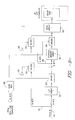
- Referring to Figure 9, there is shown in greater detail a schematic block diagram of the
bypass logic 7 shown generally in Figure 4. Figure 9 shows the associated bypass logic for one of the color bars in thejet dyeing apparatus 18. It should be understood that the same bypass logic is required for each of the color bars in the apparatus. - The
bypass logic circuitry 7 permits selective bypassing of either the look-up tables 54, staggermemory 56 or both the look-up tables 54 and staggermemories 56. This allows test patterns input over the DATA INline 44 during a diagnostic check of the system to selectively bypass certain of the components in the control system to isolate the occurence of any errors detected. - A
first bypass line 81 couples 8-bit pattern data fromline 44 into abus driver 90. Coupled after and receiving the output from the look-up table 54 is anotherbus driver 92 which provides its output to the staggermemory 56.Bus drivers memory 56.Bus drivers mode register 88. - Similar bypass circuitry is utilized with stagger
memory 56 includingbus drivers bypass line 85. - Under normal operation, the control system for each color bar operates as described above with
bus drivers line 44 is permitted to pass through each of thecomponents line bus drivers memory 56 that caused the error. When attempting to isolate an error, themode register 88 enables one or both of thebypass lines mode register 88 from the real-time computer 10. - In a prefered embodiment, each of the 16 bits loaded into
mode regsiter 88 designates a particular mode or functionning of thepattern control system 16. Thus, when the system sofware operating on the real-time computer 10 initiates a bypass of one or both of the control system components, themode register 88 receives the 16-bit data having particular bits set. A signal is then sent from themode register 88 to enable the bypass selected. - In isolation operation, the
mode register 88 provides a signal which enables the bypass bus driver and disables the driver coupled in series between a component to be bypassed and the next component to receive the pattern data. For example, if the look-up tables 54 are to be bypassed, then the signal from themode register 88disables bus driver 92 and enablesbus driver 90. Thus, the data provided online 44 flows throughbypass line 81,bus driver 90 and is input into the staggermemory 56. A similar operation occurs for bypassing the staggermemory 56 by enablingbus driver 94 and disablingbus driver 96. Likewise, to bypass both the look-up tables 54 and staggermemory 56,bus drivers mode register 88 andbus drivers - A unique advantage of the bypass feature is that it allows the test pattern data to be input directly to the
gatling memory 58 thus avoiding the time delays inherent with the operation of the staggermemory 56 as described above. The diagnostic check being performed can therefore be performed more efficiently than if the test had to wait for the staggermemory 56 to compensate for the downstream color bars. In normal day to day production operation, this technique allows the checking of jets and flows without having to wait for the stagger memory to compensate for the downstream color bars. - Referring to Figure 10, there is shown a block diagram of the look-up tables 54 associated with a single color bar as described with respect to Figure 4. It should be understood the same number of look-up tables are associated with each and every color bar in the jet dyeing apparatus.
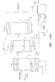
- Figure 10 shows look-up tables 1 through 512 associated with
color bar 1. The look-up tables receive input data overline 44 and output firing time data over lines 103-105. As described above, it is apparent that only one of the 512 look-up tables are used for each pattern and hence only one firing time output line 103-105 will be in use at any given time. The look-up table which is used for the pattern is selected by the look-up tableselect register 46 shown and described above with respect to Figure 4. - During a diagnostic check of the look-up tables, it is necessary to assure that the address lines operate properly, i.e., the address lines are capable of correctly specifying each unique address within each single look-up table among a group of look-up tables. To perform this check, the system software operating on the real-
time computer 10 outputs look-up table loading data in a "prime number pattern". In a preferred embodiment, the prime number pattern is selected to be the largest prime number less than the number of the addresses in each of the look-up tables. Hence, in our example, assuming each of the 512 look-up tables include 256 addresses, the prime number pattern uses theprime number 251. The system software generates a loading pattern having 251 different pieces of data. This pattern is repeated to fill up each of the look-up tables for each of the color bars. - As shown in Figure 10, look-up table 1 is loaded with data 0-250 in its first 250 addresses and loaded with
data 0 through 4 in addresses 251-255. Continuing, look-up table 2 is loaded with data 5-250 in addresses 0-245 and with data 0-8 in addresses 246-255. The system continues to load all available addresses in each of the 512 look-up tables in sequence with the same prime number pattern stream from the real-time computer 10, i.e., look-up table 1 is loaded in address 0-250 and then is loaded with the same repeating sequence data in locations 251-255, with the remaining portion of the 251 address-length prime number pattern stream being loaded into location 0-245 of the second look-up table, etc. - Accordingly, upon inputting (i.e., selecting an address within the look-up table) a "count pattern", i.e., the sequence of
binary numbers - Once all of the look-up tables have been preloaded, then the system reads each address of the look-up tables (as discused in connection with Figure 4, above) and forwards the firing time data over lines 103-105 to
comparator 102. This is accomplished byreal time computer 10, by first selecting look-up table 1 and outputting to that LUT the count pattern overbus 44, then selecting, in turn, look-up tables 2,3, etc. and outputting to those respective look-up tables the same count pattern. At the same time, the system enables an erasable programmable read only memory (EPROM) by setting the appropriate bits onmode register 88. The EPROM has stored thereon the same prime number pattern as was loaded into the look-up tables, as described above. Each byte of pattern data output by thecomputer 10 onbus 44, viabus 22, and multiplexed bymultiplexer 48, is placed on the lower address lines of the selected look-up table. The LUT in turn outputs its contents tocomparator 102, via the various lines 103-105. At the same time,EPROM 100 outputs the correspondingly numbered byte tocomparator 102. Thecomparator 102 may be of any conventional 8-bit type of comparator such as those produced by Signetics Corporation. The resulting output from thecomparator 102 online 106 reflects the coincidence of the two inputs and therefore confirms the lack of any errors in the contents of the look-up tables. It can be readily understood that by using a prime number pattern to load the look-up tables, each address location for each look-up table will have a different piece of data. This insures that any address lines causing incorrect addressing (e.g., electrically shorted or open) can be determined. - Referring back to the gatling memory shown in Figure 7, it is often necessary to test for proper operation of each of the FIFOs by insuring that each bit in the FIFO can produce a unique firing time.
- Figure 11 shows one of the FIFOs used in the
gatling memory 58. The FIFO is preferably at least a 240x8 bit FIFO which receives 240 bytes from the sequential loader (Figure 7). Each byte stored in the FIFO represents an increment of time as determined by the gatling clock described above with respect to Figure 7. The output from the FIFO eventually is sent as a serial stream of logical ones or zeros to the dye jet valve in the color bar. - Each bit in the FIFO is checked by the diagnostic system controlled by real-
time computer 10. The diagnostic system simulates a speed-up of the jet dyeing apparatus conveyor operation (by changing the contents of the simulate divisor register 84 of Figure 4) and then checks for the onset of machine "optimum speed" and machine "over-speed". These speeds are based upon the requested firing time and the operating limitations of the dye jet and will more fully be described with respect to Figures 11 and 12. - Figure 12A is a timing diagram showing the firing time for a single dye jet in one of the color bars with respect to the conveyor operating speed. Two complete cycles of operation are shown in Figure 12A wherein the dye jet has a firing time, FT, equal to 4 ms and the substrate has a travel time of 10 milliseconds (MS) per pattern line. An additional "analog" time period of .7 ms is shown appended to the firing time of 4 ms of Figure 12. This analog time represents the valve actuation or response time, i.e., the time period necessary to physically open or close the dye jet valve. It should be understood that .7 ms is only an example and that the analog time period may be greater or lesser depending upon the sophistication of the valve technology. The further shaded area adjacent to the analog time period represents a preferred operating area in which the next cycle of operation should begin. This preferred area is representing a duration of .3 ms. Again, the determination of the preferred area time period is arbitrarily based upon the efficiency required from the apparatus.
- As shown in Figures 12B-12E, when the conveyor operating speed is increased, the beginning of the next cycle of operation moves closer to the preferred operating area. Further increases in conveyor speed eventually brings the next cycle into the analog time period area. Figure 12B shows that with an increased substrate travel time of 5 ms per pattern line (as opposed to the 10 ms speed in Fig. 12A), the beginning of the next cycle occurs immediatly following the preferred operating area. Figure 12C shows the next cycle beginning in the preferred operating area with a machine speed of 4.9 ms per pattern line. The 4.9 ms per pattern line machine speed would therefore be within the "optimum speed" range. Likewise, Figure 12D shows that a machine speed of 4.8 ms per pattern line is also within the optimum speed range. Figure 12E, however, shows the next cycle of operation beginning within the analog time period. Because of valve actuation or response time limitations, the accuracy of the subsequent cycles' firing time cannot be guaranteed. Thus, the 4.4 ms per pattern line machine speed shown in Figure 12E is defined as machine "overspeed".
- It should be noted that by knowing the firing time, analog time, and preferred area time, the optimum speed and overspeed for the machine can be determined. By summing the firing time and the analog time period, the reciprocal thereof determines the machine speed in pattern lines per second. The control system detects when optimum speed and overspeed occurs and generates signals indicating when the machine is operating at these speeds. These signals are fed into real-
time computer 10 such that the real-time diagnostic software is made aware of these conditions as they occur. - Referring back to Figure 11, each of the FIFOs in the gatling memories (Figure 7) can be tested by individually setting each bit in a selected location in the FIFO and simulating the occurrence of optimum speed and overspeed through the use of the control system.
- The diagnostic for the FIFOs operates through the software in the real-time computer 10 (Figure 4) which controls the
simulator divider 84. This register is used to simulate movement of the conveyor. Thesimulator divider 84 may be of the oscillator-type wherein the 16-bits received overline 22 from the real-time computer determines an oscillating frequency. The oscillating frequency simulates transducer pulses indicating substrate travel. - An example of the diagnostic operation, assuming the gatling clock is set to provide .2 ms increments, is given with reference to Figures 11 and 12 A-12E. The FIFO output from
location 4 provides an 8-bit value having only a single bit set for testing purposes. This byte, "00001000", represents in binary form the decimal numeral "8" which, when multiplied by the gatling clock time period of .2 ms, results in a firing time of 4 ms as shown in Figures 12A-12E. Assuming a .7 ms analog time period and a .3 ms "preferred area", the system software can determine the onset of overspeed from the following equation.
Onset of Optimum Speed
= 4.0 ms/pattern line+0.7 ms+0.3 ms/pattern line
= 5.0 ms/pattern line
Onset of Overspeed
= 4.0 ms+0.7 ms
= 4.7 ms/pattern line
Overspeed > Onset of Overspeed
Onset of Overspeed > Optimum Speed > Onset of Optimum Speed
- Overspeed will thus occur if the conveyor operates at a speed greater than 4.7 ms per pattern line (onset of overspeed). The system thus operates the
simulator divider 84 to simulate an increased conveyor speed up to 4.7 ms per pattern line. As the conveyor speed approaches the 4.7 ms per pattern line speed, a signal is generated indicating that the optimum speed range has been reached. Once the simulated conveyor speed equals or becomes greater than 4.7 ms per pattern line, an overspeed signal occurs. In this manner, by individually setting each bit in the FIFO (Figure 11), the system can determine whether the bit was properly set by checking whether the onset of optimum speed and the onset of overspeed occur at the proper machine speed. - In a preferred embodiment, each FIFO is actually a set of two FIFOs, mounted in paired relation so that, while data is being read from one FIFO set, data may be written to the second member of the pair. The system software checks four machine speeds for each FIFO paired set across the width of the color bar. The system software also checks each individual FIFO in each paired set, for each color bar, using eight different firing times (which checks each bit). The system software outputs one firing time per line of data (the rest of the line contains zeros) on every other line so that only one FIFO of each FIFO set is checked at a time. While outputting this line (done every other line), the software begins to increase the simulated machine speed. First the software sets the simulated machine speed to just below the speed required to produce "optimum speed" and verifies that the "optimum speed" condition does not occur. The software then increases the simulated machine speed to just above the speed required to produce "optimum speed" and verifies that the "optimum speed" condition occurs. The software then increases the simulated machine speed to just below the threshold of the "overspeed" condition, and verifies that only the "optimum speed" condition is occurring. The simulated machine speed is then increased to the onset of the "overspeed" condition; this condition is verified. The software then proceeds to check the other side of the gatling RAM pair (to check the other side of the FIFO set), then goes to the next gatling RAM pair (across the width of the color bar), then proceeds to the next color bar, etc. until all gatling RAM's have been checked. It has been found that the firing time diagnostic dramatically increases assurances that all the hardware is operating properly.
Claims (5)
- A diagnostic circuit for a pattern control system used in a textile dyeing apparatus, comprising:a) at least one component forming part of the control system; said component receiving input information over an input bus and providing output information over an output bus;b) a bypass selection circuit coupled to the input bus and the output bus;c) a bypass selector coupled to the selection circuit and receiving selection data units for determining whether the input information or the output information from the component is to be provided to the remainder of the control system.
- A diagnostic circuit according to claim 1 wherein the bypass selection circuit comprises:
a first driver, having a first enable port and a first output port, said first driver coupled in serial with the output bus of the component;
a second driver, having a second enable port and a second output port, coupled in parallel with the component and first driver, said second driver receiving the input information from the input bus and having its second output port coupled in parallel with the first output port of the first driver; and
wherein the bypass selector provides a first signal to the first enable port and a second signal to the second enable port to selectively enable one or the other of said first and second drivers in accordance with a value of the selection data unit. - A diagnostic circuit according to claim 2 wherein the bypass selector further comprises:
a register which stores the selection data unit and powers said first or second signals in accordance with the selection data unit value. - A diagnostic circuit according to claim 2, wherein the pattern control system includes two components, each of said components having a bypass selection circuit operatively associated therewith, to enable the selective bypassing of one or the other, or both, of said two components.
- A diagnostic method for checking a plurality of address lines associated with each of a pluarlity of look-up tables in a pattern control system used in a textile dyeing apparatus, the method comprising the steps of:a) determining the number of said plurality of address lines for each of the look-up tables;b) repeatedly generating a sequence of look-up table data, said sequence having a length equal to the largest prime number less than the number of address lines for each of the look-up tables, and each piece of data in said sequence being individually unique;c) storing said sequence of look-up table data in a memory;d) loading in sequence a first of said look-up tables from its first address line to its last address line with the sequence of look-up table data; said sequence of look-up table data repeating for those address lines greater than the prime number and less than or equal to the number of address lines in the look-up table;e) loading the next of said look-up tables from its first address line to its last address line with the repeating sequence of data, said first address line of the second look-up table receiving the next piece of data in the sequence data not loaded into the previous look-up table;f) repeating step (e) for all of said plurality of look-up tables;g) generating a count pattern to address in order each of said address lines of each of said look-up tables and providing the contents thereof as a series of outputs; andh) comparing said series of outputs with the stored sequence of look-up table data to determine the coincidence of said series of outputs and the stored sequence of look-up table data.
Applications Claiming Priority (2)
| Application Number | Priority Date | Filing Date | Title |
|---|---|---|---|
| US07/487,551 US5140686A (en) | 1990-03-02 | 1990-03-02 | Diagnostic system for textile dyeing apparatus |
| US487551 | 1990-03-02 |
Publications (3)
| Publication Number | Publication Date |
|---|---|
| EP0444794A2 true EP0444794A2 (en) | 1991-09-04 |
| EP0444794A3 EP0444794A3 (en) | 1993-01-07 |
| EP0444794B1 EP0444794B1 (en) | 1997-04-23 |
Family
ID=23936204
Family Applications (1)
| Application Number | Title | Priority Date | Filing Date |
|---|---|---|---|
| EP91301122A Expired - Lifetime EP0444794B1 (en) | 1990-03-02 | 1991-02-12 | Diagnostic system for textile dyeing apparatus |
Country Status (8)
| Country | Link |
|---|---|
| US (1) | US5140686A (en) |
| EP (1) | EP0444794B1 (en) |
| JP (1) | JPH04214463A (en) |
| AT (1) | ATE152262T1 (en) |
| AU (1) | AU636007B2 (en) |
| CA (1) | CA2036349C (en) |
| DE (1) | DE69125743D1 (en) |
| NZ (1) | NZ237252A (en) |
Families Citing this family (6)
| Publication number | Priority date | Publication date | Assignee | Title |
|---|---|---|---|---|
| JPH04284511A (en) * | 1991-03-14 | 1992-10-09 | Toyota Motor Corp | Abnormality detector for programmable controller |
| US5425389A (en) * | 1993-07-08 | 1995-06-20 | Milliken Research Corporation | Method and apparatus for contiguous valve control |
| US6061283A (en) * | 1998-10-23 | 2000-05-09 | Advantest Corp. | Semiconductor integrated circuit evaluation system |
| US6124696A (en) * | 1999-07-14 | 2000-09-26 | Lexmark International, Inc. | Programmable stepper motor controller and method therefor |
| GB0321164D0 (en) * | 2003-09-10 | 2003-10-08 | Hewlett Packard Development Co | Methods,apparatus and software for printing location pattern |
| US7948786B2 (en) * | 2008-02-06 | 2011-05-24 | Micron Technology, Inc. | Rank select using a global select pin |
Citations (5)
| Publication number | Priority date | Publication date | Assignee | Title |
|---|---|---|---|---|
| US4039813A (en) * | 1976-04-07 | 1977-08-02 | Sperry Rand Corporation | Apparatus and method for diagnosing digital data devices |
| GB2085171A (en) * | 1980-10-09 | 1982-04-21 | Control Data Corp | Lsi chip logic testing system resident on an lsi chip |
| EP0289158A2 (en) * | 1987-04-20 | 1988-11-02 | Tandem Computers Incorporated | Diagnostic apparatus for a data processing system |
| EP0340895A2 (en) * | 1988-04-29 | 1989-11-08 | International Business Machines Corporation | Improvements in logic and memory circuit testing |
| US4979380A (en) * | 1989-09-12 | 1990-12-25 | Sakowski And Robbins Corporation | Automated dye pattern application system |
Family Cites Families (4)
| Publication number | Priority date | Publication date | Assignee | Title |
|---|---|---|---|---|
| US3901273A (en) * | 1973-04-09 | 1975-08-26 | Leesona Corp | Fluid control system with on-line diagnosis means isolating malfunctions |
| DE3719497A1 (en) * | 1987-06-11 | 1988-12-29 | Bosch Gmbh Robert | SYSTEM FOR TESTING DIGITAL CIRCUITS |
| JP2521774B2 (en) * | 1987-10-02 | 1996-08-07 | 株式会社日立製作所 | Memory-embedded logic LSI and method for testing the LSI |
| JPH01132980A (en) * | 1987-11-17 | 1989-05-25 | Mitsubishi Electric Corp | Electronic circuit with test function |
-
1990
- 1990-03-02 US US07/487,551 patent/US5140686A/en not_active Expired - Lifetime
-
1991
- 1991-02-12 DE DE69125743T patent/DE69125743D1/en not_active Expired - Lifetime
- 1991-02-12 EP EP91301122A patent/EP0444794B1/en not_active Expired - Lifetime
- 1991-02-12 AT AT91301122T patent/ATE152262T1/en not_active IP Right Cessation
- 1991-02-14 CA CA002036349A patent/CA2036349C/en not_active Expired - Fee Related
- 1991-02-18 AU AU71120/91A patent/AU636007B2/en not_active Ceased
- 1991-02-27 NZ NZ237252A patent/NZ237252A/en unknown
- 1991-03-01 JP JP3059470A patent/JPH04214463A/en active Pending
Patent Citations (5)
| Publication number | Priority date | Publication date | Assignee | Title |
|---|---|---|---|---|
| US4039813A (en) * | 1976-04-07 | 1977-08-02 | Sperry Rand Corporation | Apparatus and method for diagnosing digital data devices |
| GB2085171A (en) * | 1980-10-09 | 1982-04-21 | Control Data Corp | Lsi chip logic testing system resident on an lsi chip |
| EP0289158A2 (en) * | 1987-04-20 | 1988-11-02 | Tandem Computers Incorporated | Diagnostic apparatus for a data processing system |
| EP0340895A2 (en) * | 1988-04-29 | 1989-11-08 | International Business Machines Corporation | Improvements in logic and memory circuit testing |
| US4979380A (en) * | 1989-09-12 | 1990-12-25 | Sakowski And Robbins Corporation | Automated dye pattern application system |
Also Published As
| Publication number | Publication date |
|---|---|
| AU636007B2 (en) | 1993-04-08 |
| CA2036349A1 (en) | 1991-09-03 |
| EP0444794B1 (en) | 1997-04-23 |
| NZ237252A (en) | 1995-04-27 |
| US5140686A (en) | 1992-08-18 |
| JPH04214463A (en) | 1992-08-05 |
| EP0444794A3 (en) | 1993-01-07 |
| ATE152262T1 (en) | 1997-05-15 |
| CA2036349C (en) | 1996-09-10 |
| DE69125743D1 (en) | 1997-05-28 |
| AU7112091A (en) | 1991-09-05 |
Similar Documents
| Publication | Publication Date | Title |
|---|---|---|
| EP0389109B1 (en) | Data loading and distributing process and apparatus for control of a patterning process | |
| JP3184546B2 (en) | Patterning method and apparatus for forming a dye pattern having a pattern element matrix having a plurality of pattern elements in each of a plurality of pattern rows for a dye fabric of a textile material | |
| NZ237255A (en) | Distributing dye pattern data using memory access controller | |
| US3832535A (en) | Digital word generating and receiving apparatus | |
| US4033154A (en) | Electronic control system for dyeing and printing materials | |
| US5140686A (en) | Diagnostic system for textile dyeing apparatus | |
| US4321687A (en) | Timing pulse generation | |
| EP1419473B1 (en) | Reproduction of colored images on absorbent substrates using color blending techniques | |
| US7394555B2 (en) | Digital control system | |
| EP0042511B1 (en) | Control system and method for testing the operation of print hammers | |
| KR890014805A (en) | Central control method of loom | |
| NZ264507A (en) | Textile dyeing pattern control system diagnostic circuit | |
| AU633180B2 (en) | Process and apparatus allowing the real-time distribution of data for control of a patterning process | |
| US4273041A (en) | Belt printer control architecture | |
| GB2173930A (en) | Physical modelling device for use with computer-aided design | |
| US4559620A (en) | Mass memory system addressing circuit | |
| CA1250370A (en) | Method and apparatus for addressing a memory by array transformations | |
| US5425389A (en) | Method and apparatus for contiguous valve control | |
| HU211380B (en) | Method and apparatus for transporting media of measured quantity | |
| SU1357960A1 (en) | Device for checking quantity of units of binary code by modulus k | |
| SU978154A1 (en) | Device for checking digital units | |
| Beck et al. | Auxiliary CAMAC crate controllers using a 16 bit microprocessor: Applications in accelerator control |
Legal Events
| Date | Code | Title | Description |
|---|---|---|---|
| PUAI | Public reference made under article 153(3) epc to a published international application that has entered the european phase |
Free format text: ORIGINAL CODE: 0009012 |
|
| AK | Designated contracting states |
Kind code of ref document: A2 Designated state(s): AT BE CH DE DK ES FR GB GR IT LI LU NL SE |
|
| PUAL | Search report despatched |
Free format text: ORIGINAL CODE: 0009013 |
|
| AK | Designated contracting states |
Kind code of ref document: A3 Designated state(s): AT BE CH DE DK ES FR GB GR IT LI LU NL SE |
|
| 17P | Request for examination filed |
Effective date: 19930215 |
|
| 17Q | First examination report despatched |
Effective date: 19951011 |
|
| GRAG | Despatch of communication of intention to grant |
Free format text: ORIGINAL CODE: EPIDOS AGRA |
|
| GRAH | Despatch of communication of intention to grant a patent |
Free format text: ORIGINAL CODE: EPIDOS IGRA |
|
| GRAH | Despatch of communication of intention to grant a patent |
Free format text: ORIGINAL CODE: EPIDOS IGRA |
|
| GRAA | (expected) grant |
Free format text: ORIGINAL CODE: 0009210 |
|
| AK | Designated contracting states |
Kind code of ref document: B1 Designated state(s): AT BE CH DE DK ES FR GB GR IT LI LU NL SE |
|
| PG25 | Lapsed in a contracting state [announced via postgrant information from national office to epo] |
Ref country code: IT Free format text: LAPSE BECAUSE OF FAILURE TO SUBMIT A TRANSLATION OF THE DESCRIPTION OR TO PAY THE FEE WITHIN THE PRE;WARNING: LAPSES OF ITALIAN PATENTS WITH EFFECTIVE DATE BEFORE 2007 MAY HAVE OCCURRED AT ANY TIME BEFORE 2007. THE CORRECT EFFECTIVE DATE MAY BE DIFFERENT FROM THE ONE RECORDED.SCRIBED TIME-LIMIT Effective date: 19970423 Ref country code: CH Effective date: 19970423 Ref country code: BE Effective date: 19970423 Ref country code: FR Effective date: 19970423 Ref country code: GR Free format text: LAPSE BECAUSE OF FAILURE TO SUBMIT A TRANSLATION OF THE DESCRIPTION OR TO PAY THE FEE WITHIN THE PRESCRIBED TIME-LIMIT Effective date: 19970423 Ref country code: ES Free format text: THE PATENT HAS BEEN ANNULLED BY A DECISION OF A NATIONAL AUTHORITY Effective date: 19970423 Ref country code: AT Effective date: 19970423 Ref country code: DK Effective date: 19970423 Ref country code: LI Effective date: 19970423 Ref country code: NL Effective date: 19970423 |
|
| REF | Corresponds to: |
Ref document number: 152262 Country of ref document: AT Date of ref document: 19970515 Kind code of ref document: T |
|
| REG | Reference to a national code |
Ref country code: CH Ref legal event code: EP |
|
| REF | Corresponds to: |
Ref document number: 69125743 Country of ref document: DE Date of ref document: 19970528 |
|
| PG25 | Lapsed in a contracting state [announced via postgrant information from national office to epo] |
Ref country code: SE Effective date: 19970723 |
|
| PG25 | Lapsed in a contracting state [announced via postgrant information from national office to epo] |
Ref country code: DE Effective date: 19970724 |
|
| EN | Fr: translation not filed | ||
| NLV1 | Nl: lapsed or annulled due to failure to fulfill the requirements of art. 29p and 29m of the patents act | ||
| REG | Reference to a national code |
Ref country code: CH Ref legal event code: PL |
|
| PG25 | Lapsed in a contracting state [announced via postgrant information from national office to epo] |
Ref country code: LU Free format text: LAPSE BECAUSE OF NON-PAYMENT OF DUE FEES Effective date: 19980212 Ref country code: GB Free format text: LAPSE BECAUSE OF NON-PAYMENT OF DUE FEES Effective date: 19980212 |
|
| PLBE | No opposition filed within time limit |
Free format text: ORIGINAL CODE: 0009261 |
|
| STAA | Information on the status of an ep patent application or granted ep patent |
Free format text: STATUS: NO OPPOSITION FILED WITHIN TIME LIMIT |
|
| 26N | No opposition filed | ||
| GBPC | Gb: european patent ceased through non-payment of renewal fee |
Effective date: 19980212 |