EP0444702A2 - Superconducting coil and process for manufacturing the same, composite superconductor and process for manufacturing the same and superconducting apparatus - Google Patents
Superconducting coil and process for manufacturing the same, composite superconductor and process for manufacturing the same and superconducting apparatus Download PDFInfo
- Publication number
- EP0444702A2 EP0444702A2 EP91103113A EP91103113A EP0444702A2 EP 0444702 A2 EP0444702 A2 EP 0444702A2 EP 91103113 A EP91103113 A EP 91103113A EP 91103113 A EP91103113 A EP 91103113A EP 0444702 A2 EP0444702 A2 EP 0444702A2
- Authority
- EP
- European Patent Office
- Prior art keywords
- superconducting
- composite
- superconducting coil
- superconductors
- superconductor
- Prior art date
- Legal status (The legal status is an assumption and is not a legal conclusion. Google has not performed a legal analysis and makes no representation as to the accuracy of the status listed.)
- Withdrawn
Links
Images

Classifications
-
- H—ELECTRICITY
- H01—ELECTRIC ELEMENTS
- H01F—MAGNETS; INDUCTANCES; TRANSFORMERS; SELECTION OF MATERIALS FOR THEIR MAGNETIC PROPERTIES
- H01F41/00—Apparatus or processes specially adapted for manufacturing or assembling magnets, inductances or transformers; Apparatus or processes specially adapted for manufacturing materials characterised by their magnetic properties
- H01F41/02—Apparatus or processes specially adapted for manufacturing or assembling magnets, inductances or transformers; Apparatus or processes specially adapted for manufacturing materials characterised by their magnetic properties for manufacturing cores, coils, or magnets
- H01F41/04—Apparatus or processes specially adapted for manufacturing or assembling magnets, inductances or transformers; Apparatus or processes specially adapted for manufacturing materials characterised by their magnetic properties for manufacturing cores, coils, or magnets for manufacturing coils
- H01F41/048—Superconductive coils
-
- H—ELECTRICITY
- H01—ELECTRIC ELEMENTS
- H01F—MAGNETS; INDUCTANCES; TRANSFORMERS; SELECTION OF MATERIALS FOR THEIR MAGNETIC PROPERTIES
- H01F6/00—Superconducting magnets; Superconducting coils
- H01F6/06—Coils, e.g. winding, insulating, terminating or casing arrangements therefor
Definitions
- the present invention relates to a superconducting coil and a process for manufacturing the same, a composite superconductor forming the superconducting coil and a process for manufacturing the same and a superconducting apparatus having the superconducting coil incorporated therein.
- the composite superconductor generally comprises superconductors and normal conductors.
- the composite superconductor is formed into a round section wire, a square section wire, or a hollow wire, for example, by embedding superconductor wire elements having a diameter of 5 ⁇ m to 250 ⁇ m into a normal conductor formed of steel, alminium or other metals or an alloy of these metals.
- Another composite superconductor which is coated with a copper oxide coating on the outermost surface thereof so that it can be immersed into a liquid refrigerant.
- a composite superconductor which is coated with a copper oxide coating on the outermost surface thereof is known as an example of a composite superconductor which is immersed into a liquid coolant is known (refer to JP-B-Sho 64-10887).
- a superconductor which are formed with a multiplicity of grooves and walls on the surface skin band of cooling area by cutting to increase the cooling area so that lowering of performance due to burn-out phenomenon is prevented has been proposed (refer to JP-A-Sho 55-56306).
- the above mentioned objects are accomplished by forming a thin resin coating on the surface of the composite superconductor and disposing spacers between the conductors.
- a technique using a copper oxide coating is characterized in that the outermost stabilizing portion of the composite superconductor is formed of copper and a copper oxide coating is formed on the surface of the outermost portion for enhancing the cooling performance.
- the metal surrounding superconducting wire elements which are structural members of the composite superconductor is limited to copper.
- a chemical treatment or electrolytic process using chromic acid, potassium permanganate and the like is used for forming a coating film. However, these process have a problem of processing of chemical waste liquids. Solution of this problem has been demanded in view of protection of environment.
- the proposal to increase the cooled area has the possibility that raised portions formed on the cooling area may be partly omitted in use of an actual apparatus using the superconductor.
- a thin coating film mainly formed of a high-molecular material is formed on the surfaces of composite superconductors including the cooling surfaces thereof and a cooling fluid is admitted between the cooling surfaces of the superconductors for stabilizing the cooling performance.
- the present invention is realized by a combination of the formation of a thin resin coating on the surfaces of the composite superconductors and the interposition of spacers between the conductors.
- a superconducting coil of the present invention is formed by winding composite superconductors which are coated with an insulating material therearound and wound.
- the insulating material is a resin. Further insulative spacer members are interposed between the composite superconductors coated with the resin.
- a superconducting coil of the present invention is formed by winding composite superconductors which include combined plural superconducting wire elements and normal conductors.
- the composite superconductors are coated with a resin therearound and spacers are interposed between the resin coated composite superconductors.
- a superconducting coil of the present invention is formed by winding composite superconductors coated with a resin while refrigerant paths are assured between the composite superconductors.
- a composite superconductor of the present invention comprises composite superconducting wires coated with a resin, a part of the coated surface of the wires being additionally provided with an insulating member.
- a process for manufacturing a superconducting coil includes winding composite superconductors which are coated with an insulating film on the surface thereof by an electrocoating method. If it is necessary to repair damaged portion of the insulating film occurred when the composite conductor is formed into the shape of coil, the electrocoating may be performed again after forming into the shape of coil.
- a process for manufacturing a superconducting coil of the present invention comprises the steps of winding composite superconductors into the shape of coil; and performing an electrocoating to form an insulating film on the surface of the coil.
- a process of manufacturing a composite superconductor comprises the steps of combining a superconductor with a normal conductor; and electrocoating the entire surface of the combined conductor with a high-molecular resin.
- the applied voltage is 10 to 200 volts and the electrocoating time is 30 to 150 seconds.
- a way of combining conducting wire elements with normal conductors includes ways as follows:
- a normal conductor having a low electric resistance is preferable since the normal conductor becomes a by-pass even if a superconductor is partially destroyed. Therefore, use of pure metal such as oxygen-free copper and silver is preferable.
- the materials of superconducting wire element are not particularly limited. Accordingly, intermetallic compounds such as Nb3Sn and alloys such as NbTi may be used to cope with cryogenic temperatures (use of liquid helium). Even oxide ceramics system superconducting materials represented by Y-Ba-Cu-O may be used at temperatures above that of liquid nitrogen.
- preferable thickness of the coating film depends upon the service environment, thinner coating film is generally better. Preferable range is 1 to 30 ⁇ m. Uniform coating is preferable. The present inventors have found that an electrocoating method which will be described hereafter is most preferable to provide a preferable coating.
- high-molecular resin includes epoxy resins, acrylic resins, fluorine resins, phenolic resins and polybuthadiene resins.
- an excellent effect of the present invention is achieved when an epoxy resin is used.
- a superconducting apparatus of the present invention comprises a superconducting coil which is formed by winding insulating material coated composite superconductors and is in contact with a liquid coolant.
- the insulating material forms a resin coating film. Spacings between the wound composite superconductors themselves are maintained by spacer members.
- the liquid refrigerant includes liquid helium, liquid nitrogen, liquid oxygen and the like.
- the superconducting apparatus of the present invention is designed to be cooled by boiling. Accordingly, all the portions between resin coated composite superconductors themselves excepting the spacer members should be areas to be cooled by the liquid refrigerant. That is, a structure in which the coated composite superconductors themselves directly contact with each other is eliminated so that the spacer members are necessarily interposed or liquid refrigerant flow paths are formed between the resin coated composite superconductors.
- the electrocoating method comprises the steps of; blending a high-molecular material such as an epoxy resin, acrylic resin in an aqueous solution; precipitating the resin on the surface of a piece to be coated which is formed of an electrically conductive material based on an electrophoretic principle; and baking the coated piece to form a firm insulating film thereon.
- This method makes it possible to coat an electrically conductive portion with a coating film having an uniform thickness.
- the resin used for this coating method is blended in an aqueous solution.
- the blending ratio of water is about 70 to 80% by weight.
- This coating method is excellent in that the resin can be removed from the waste liquid by various filters and excellent in safety of working and environmental protection.
- Such an electrocoating is generally performed in a batch manner.
- pieces to be coated according to the present invention are often linear and the length thereof is generally not less than several meters. Therefore, since conventional batch type processing can not coat the whole of linear piece to be coated, a process for electrocoating linear pieces was devised.
- electrocoating is suitably performed while the whole of the composite superconductor wound into a coil shape is immersed in an electrocoating bath.
- a high-molecular resin can be used as an insulating material and the whole or a part of the composite superconductor can be coated with a coating film having a given, thin and uniform thickness. Accordingly, a sufficient cooling thermal flow flux is assured so that a stable superconducting state may be attained depending upon an applied magnetic field.
- the coating resin has a high heat resistance. Since the thickness of the resin film is substantially proportional to the breakdown voltage of an electric insulation, the thinner coating film provides the less insulation.
- spacer members are interposed. Accordingly, insulation is kept while flow paths of liquid refrigerant are assured and heat resistance is improved so that excellent boiling cooling can be expected.
- a superconducting coil, a composite superconductor and a superconducting apparatus which are stable and excellent in cooling-performance can be provided. Since an uniform resin coating is formed by an electrocoating in the present invention, damage to coating and short-circuiting will not occur. Processes for manufacturing a superconducting coil and a composite superconductor of the present invention does not require a waste liquid processing.
- the epoxy resin coating has an excellent adhesion to superconducting materials in comparison with the other resin coatings (for example, acrylic resins and fluorine resins) so that omittion is hard to occur.
- the epoxy resin is quickly dried and easy to be molded as general features and has advantages that it is easily available and inexpensive.
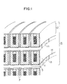
- Fig. 1 is a sectional in part and perspective view of a superconducting coil 15 comprising a plurality of stacked pancakes 12, each being formed by concentrically winding a high capacity linear composite superconductors each having a square section to provide inner diameter of a central hollow space of 200 mm and an outer diameter of about 500 mm.
- a perspective view of the superconducting coil 15 is shown in Fig. 2.
- the superconducting coil 15 of the present embodiment is formed by stacking 12 pancakes.
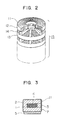
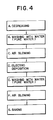
- the superconducting coil 15 is manufactured according to following steps. The process for manufacturing the high capacity composite superconductor 11 will now be described with reference to Fig. 3.
- a superconducting wire element which is a bundle of 1060 filaments formed of NbTi having a diameter 50 ⁇ m is inserted into an oxigen-free copper pipe, from which the wire is extruded for drawing working. Thereafter, 10 molded strands, which are formed by being subjected to aging heat treatment are inserted into a recess of a stabilized block 2 of oxygen-free copper having a ⁇ -shaped section which is formed by hot extrusion. Then, the stranded wires 1 are pressed by a lid 3 and fixed by a solder 4. The sectional dimension of the superconductor 11 in such a condition is 12.6 mm x 26.8 mm. The superconductor is then coated with an insulating film 7 over an entire of the outer periphery thereof. An electrocoating method is used for applying the insulting film 7.
- treating bathes one for each step of a process shown in Fig. 4 are aligned.
- the material to be coated is successively subjected to coating treatment.
- Epoxy cation electrocoating material for example, Aqua No. 4200 manufactured by Nippon Yushi Co., Ltd.
- Aqua No. 4200 manufactured by Nippon Yushi Co., Ltd. is used as an electrocoating paint.
- the length of a baking electric furnace is 5 m in view of conductor winding up speed and heating time.
- the conditions of Table 1 excellent in smoothness are applied in consideration of independently determined thin film coating conditions.
- the length of degreasing and washing baths in a direction of passing of a piece to be coated which are used at steps shown in Fig. 4 is 0.3 m.
- the spacing of 0.1 m is provided between the baths and a spacing of 0.5 m is provided for an air blowing station.
- the length of an electrocoating bath is 0.5 mm.
- a spacing of 0.1 m is provided between the electrocoating bath and a washing bath at next step is 0.1 m. Pure water contained in the electrocoating liquid is dropped in the spacing to preliminarily wash the coated conductor to remove residual electrocoating liquid which has formed no coating film.
- the washing bath is 0.5 m in length.
- the water in the bath is stirred by using a circulating pump. After washing the conductor with water, the range of air blowing for removing water droplets is 0.3 m, and the range of temperature gradient up to a baking furnace temperature of 175°C is 0.3 m.
- Each bath is double-structured.
- a sponge-like seal member is disposed at each of outlet and inlet for preventing leakage of liquid therefrom to the inside of an inner treatment bath. The liquid leaked in spite of such a provision is recovered into an outer bath and is circulated by the circulating pump.
- the level of the treating liquid is maintained above the upper side of a piece to be coated by using the discharging pressure of the circulating pump so that the treating liquid normally covers the superconductor.
- Roller electrodes are disposed in front of the degreasing bath for conducting a current to the piece to be coated.
- the insulator 5 made of FRP (glass fiber reinforced epoxy resin) having a section of 0.2 mm x 25 mm is disposed on the side of the superconductor with which the other superconductor contacts as shown in Fig. 3.
- the insulator 5 is disposed since the electric resistance of the insulating film 7 coated over the outer periphery of the superconductor 11 is so low that insulation between the superconductors is insufficient if the coating thickness is low.
- the insulator 5 functions as a spacer member.
- the superconducting coil 15 is thus formed by stacking 12 these pancakes 12.
- spacers 13, each formed of bar-like insulator radially extending from the inner radial side to outer radial side thereof are disposed between adjacent pancakes 12 to provide spacings through which liquid helium passes 14.
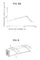
- the superconducting coil 15 which is formed by the above mentioned steps is immersed in liquid helium at an atomospheric pressure so that helium boiling characteristics is measured for evaluating the heat conduction characteristics thereof. Boiling characteristics is measured for different film thicknesses as shown in Fig. 5A. Comparison of a curve (i) of uncoated specimen with a curve (ii) of a specimen coated with a 1.5 ⁇ m thick insulating film of the present embodiment shows that a slight increase in temperature difference (between the conductor temperature T cond and the helium temperature T He ) increases a minimum value of heat flow flux : q min by about 0.18.
- a curve (iii) represents the heat conduction characteristics of a specimen coated with a 5 ⁇ m thick coating film according to the electrocoating method.
- qmin 0.24 w/cm2 was obtained at a temperature difference equivalent to a critical temperature Tc of superconduction.
- Curves (iV) and (V) represent heat conduction characteristics of specimen coated with 17 ⁇ m and 40 ⁇ m thick coating films, respectively.
- coating film thickness provides a stable coating film according to electrocoating method.
- preferable range of the coating film thickness of the composite superconductor is 1 ⁇ m to 30 ⁇ m in the present embodiment, it is preferable that the heat flow rate be higher and that the coating film thickness be 5 ⁇ m to 20 ⁇ m in view of and manufacturing conditions and process control.
- an effective heat flow flux q e used for the design of superconductor is determined as shown in Fig. 5B.
- a way of determining q e relies upon Madoc's equi-area law (The Institute of Electrical Engineers of Japan Daigaku-Koza, Superconductivity engineering, revised page 105, 1988 published by the Institute of Electrical Engineers of Japan).
- a value q e increases with an increase in the thickness of the coating film. When the thickness exceeds 18 ⁇ m, the heat resistance in the coating film becomes predominant so that q e decreases with an increase in thickness.
- Measuring is conducted under conditions that the superconductor is formed of a niobium and titanium alloy, the strength of applied magnetic field was 8 Tesla; the ratio of conducting current to critical current is 0.5. It is understood from Fig. 5B that a value of coating film thickness (about 18 ⁇ m) gives a maximum q e and that a higher q e value is preferably obtained if the thickness is 5 to 20 ⁇ m.
- epoxy resins in the present embodiment is described in detail, use of acrylic resins, fluorine resins, phenol resins and polybutadiene resins may provide equivalent effects.
- the applied voltage and the electrocoating time fall in the ranges 10 to 200 volts and 30 to 150 seconds, respectively if each of these resins is formed into the above-mentioned thickness.
- the applied voltage is changed to 50 V (electrocoating time: 150 seconds) and 200 V (150 seconds), respectively.
- the coating film 7 covering the superconductor 11 is formed of enamel and a dip coating method in which a superconductor is immersed into a high-molecular material solution and then pulled out for curing is used for applying the insulating film, similar result is obtained.
- the linear composite superconductor 11 which is manufactured in Embodiment 1 is concentrically wound to manufacture pancakes 12, each having, for example, an inner diameter of 200mm and an outer diameter of 500 mm.
- the superconducting coil 15 comprises one or plurality of stacked pancakes 12.
- the thickness of an annular plate forming each pancake is 26.8 mm.
- the number of stacks of the superconductor is 12.
- Bar-like spacers 13 radially extending from the inner to outer side are disposed between the adjacent pancakes 12 so that spacings 14 through which liquid helium passes.
- the resin is selectively deposited to a portion of the insulating film which is damaged on forming the pancakes and through which normally conductive material is exposed resulting in that pancakes for superconducting coil having a damage-free insulating film can be manufactured.
- an insulator 5 for preventing the superconductor 11 from contacting with the other superconductor is preliminarily wound around the superconductor 11 as shown in Fig. 6. Thereafter, the pancakes are concentrically formed in the present embodiment.
- the insulator 5 is a polyimide tape is having a width of 15 mm in the present embodiment. If the insulator 5 is adhered to the superconductor 11 with an adhesive and the like when the insulator 5 is wound around the superconductor 11, subsequent working become easier.
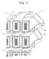
- FIG. 7 A sectional in part and perspective view of a superconducting coil formed of the above mentioned superconductor 11 is shown in Fig. 7.
- the boiling characteristics of the superconductor substantially corresponds to the curve (iii) in Fig. 5A when the insulating film 7 is 5 ⁇ m in thickness.
- the surface area of the insulator 5 covering the superconductor 11 is lower than that of the embodiment 1 and the migration of the boiling liquid is possible in a direction of thickness of the pancake 12.
- a boiling type superconducting device which uses the superconducting coil 15 of the embodiment 1 is exemplarily shown in Fig. 8.
- the superconducting coil 15 in which spacings 14 through which liquid helium passes are formed between the pancakes 12 is immersed in liquid helium 17.
- the superconducting coil 15 is supported by a support 16 and is connected to current terminals 19.
- a helium container 21 containing liquid helium 17 is provided with a liquid helium charging and discharging port 24 at the upper side thereof.
- the helium container 21 is surrounded by a heat shielding plate 22 on the outer peripheral side thereof.
- the heat shielding plate 22 is surrounded by a vacuum container 23 on the outer side thereof.
- Vacuum adiabatic chambers 20 are defined between the helium container 21 and the heat shielding plate 22; the heat shielding plate 22 and the vacuum container 23.
- a support 16 for supporting a compression load is provided on the lower side of each chamber.
- a support 18 is provided to support a tensile load on the upper side thereof.
- the electrocoating method is most safe among various coating methods and the manufacturing cost is low since the ratio of water in the coating material is about 75%.
- Mb3Sn is used as a superconductive material for liquid helium in the above mentioned embodiments
- the present invention is not limited to only this material and may be applicable to any other superconductive materials and liquid refrigerant. If a superconductor comprising, for example, perovskite superconducting wires which are surrounded by a stable metal such as silver and then coated with a resin is used together with an insulator and spacer members, a liquid refrigerant at a temperature equal to or above the temperature of the liquid nitrogen may be used.
Landscapes
- Engineering & Computer Science (AREA)
- Power Engineering (AREA)
- Manufacturing & Machinery (AREA)
- Superconductors And Manufacturing Methods Therefor (AREA)
Abstract
A superconducting coil (15) is formed by coating a composite superconductor (11) with a resin thereon and winding the coated superconductor. A coating film (7) of the resin is formed by a electrocoating method. The resin is selected from a group consisting of epoxy resins, acrylic resins, fluorine resins, phenolic resins and polybutadiene resins. <IMAGE>
Description
- The present invention relates to a superconducting coil and a process for manufacturing the same, a composite superconductor forming the superconducting coil and a process for manufacturing the same and a superconducting apparatus having the superconducting coil incorporated therein.
- The composite superconductor generally comprises superconductors and normal conductors. The composite superconductor is formed into a round section wire, a square section wire, or a hollow wire, for example, by embedding superconductor wire elements having a diameter of 5 µm to 250 µm into a normal conductor formed of steel, alminium or other metals or an alloy of these metals.
- As composite superconductor having an outermost portion around which a resin tape is wound has heretofore been known. However, the thickness of the resin tape is so thick that it functions only an insulating member since this composite superconductor is designed to be immersed in a liquid refrigerant.
- Another composite superconductor which is coated with a copper oxide coating on the outermost surface thereof so that it can be immersed into a liquid refrigerant.
- Further, a composite superconductor which is coated with a copper oxide coating on the outermost surface thereof is known as an example of a composite superconductor which is immersed into a liquid coolant is known (refer to JP-B-Sho 64-10887).
- On the other hand, processes for coating the superconductor with a resin in lieu of tape by a dipping coating have been proposed (refer to JP-A-Hei 1-183008, Hei 1-251517, Sho 63-281316, Sho 64-7414, Sho 61-214305, Sho 64-19613).
- A superconductor which are formed with a multiplicity of grooves and walls on the surface skin band of cooling area by cutting to increase the cooling area so that lowering of performance due to burn-out phenomenon is prevented has been proposed (refer to JP-A-Sho 55-56306).
- It is an object of the present invention to realize a superconducting coil which is excellent in cooling performance, a composite superconductor and a process for manufacturing the same and a superconducting apparatus which are excellent in cooling performance.
- It is another object of the present invention to realize a superconducting coil, a composite superconductor and a superconducting apparatus in which damage to the coating and short-circuiting will not occur.
- It is a further object of the present invention to realize a superconducting coil and a composite superconductor which do not substantially require any waste liquid processing.
- The above mentioned objects are accomplished by forming a thin resin coating on the surface of the composite superconductor and disposing spacers between the conductors.
- A process to the present invention will now be described.
- A technique using a copper oxide coating is characterized in that the outermost stabilizing portion of the composite superconductor is formed of copper and a copper oxide coating is formed on the surface of the outermost portion for enhancing the cooling performance. However, the metal surrounding superconducting wire elements which are structural members of the composite superconductor is limited to copper. A chemical treatment or electrolytic process using chromic acid, potassium permanganate and the like is used for forming a coating film. However, these process have a problem of processing of chemical waste liquids. Solution of this problem has been demanded in view of protection of environment.
- Therefore, resin coating is more preferable. However a desired coating thickness cannot be obtained by conventional resin coating processes. In other words, conventional coating processes provide more thick coating film than that needed and partially ununiform coating film. These disadvantages are caused by dipping method. The dipping method would of course be an effective technique if these disadvantages would be eliminated.
- The proposal to increase the cooled area has the possibility that raised portions formed on the cooling area may be partly omitted in use of an actual apparatus using the superconductor.
- Due to poor heat conduction of the resin coating film, the thicker the coating film becomes, the higher the heat resistance of the coating film becomes, the more difficult it become to conduct the low temperature of a liquid refrigerant to the superconductor. However, if the coating film becomes too thinner, damages to the coating film and short-circuiting between the superconducting wires becomes liable to occur.
- In accordance with the present invention, a thin coating film mainly formed of a high-molecular material is formed on the surfaces of composite superconductors including the cooling surfaces thereof and a cooling fluid is admitted between the cooling surfaces of the superconductors for stabilizing the cooling performance.
- The present invention is realized by a combination of the formation of a thin resin coating on the surfaces of the composite superconductors and the interposition of spacers between the conductors.
- The present invention will now be described.
- A superconducting coil of the present invention is formed by winding composite superconductors which are coated with an insulating material therearound and wound. The insulating material is a resin. Further insulative spacer members are interposed between the composite superconductors coated with the resin.
- A superconducting coil of the present invention is formed by winding composite superconductors which include combined plural superconducting wire elements and normal conductors. The composite superconductors are coated with a resin therearound and spacers are interposed between the resin coated composite superconductors.
- A superconducting coil of the present invention is formed by winding composite superconductors coated with a resin while refrigerant paths are assured between the composite superconductors.
- A composite superconductor of the present invention comprises composite superconducting wires coated with a resin, a part of the coated surface of the wires being additionally provided with an insulating member.
- A process for manufacturing a superconducting coil includes winding composite superconductors which are coated with an insulating film on the surface thereof by an electrocoating method. If it is necessary to repair damaged portion of the insulating film occurred when the composite conductor is formed into the shape of coil, the electrocoating may be performed again after forming into the shape of coil.
- A process for manufacturing a superconducting coil of the present invention comprises the steps of winding composite superconductors into the shape of coil; and performing an electrocoating to form an insulating film on the surface of the coil.
- A process of manufacturing a composite superconductor comprises the steps of combining a superconductor with a normal conductor; and electrocoating the entire surface of the combined conductor with a high-molecular resin.
- When the electrocoating of the composite superconductor is successively performed, the applied voltage is 10 to 200 volts and the electrocoating time is 30 to 150 seconds.
- A way of combining conducting wire elements with normal conductors includes ways as follows:
- 1. A plurality of superconducting wire elements are surrounded by a normal conductor.
- 2. Superconducting wire elements are disposed around a normal conductor.
- 3. A plurality of wires formed of a normal conductive material and a plurality of superconducting wire elements are stranded so that they coexist.
- A normal conductor having a low electric resistance is preferable since the normal conductor becomes a by-pass even if a superconductor is partially destroyed. Therefore, use of pure metal such as oxygen-free copper and silver is preferable.
- The materials of superconducting wire element are not particularly limited. Accordingly, intermetallic compounds such as Nb₃Sn and alloys such as NbTi may be used to cope with cryogenic temperatures (use of liquid helium). Even oxide ceramics system superconducting materials represented by Y-Ba-Cu-O may be used at temperatures above that of liquid nitrogen.
- Although preferable thickness of the coating film depends upon the service environment, thinner coating film is generally better. Preferable range is 1 to 30 µm. Uniform coating is preferable. The present inventors have found that an electrocoating method which will be described hereafter is most preferable to provide a preferable coating.
- Specific example of high-molecular resin includes epoxy resins, acrylic resins, fluorine resins, phenolic resins and polybuthadiene resins. In particular, an excellent effect of the present invention is achieved when an epoxy resin is used.
- A superconducting apparatus of the present invention comprises a superconducting coil which is formed by winding insulating material coated composite superconductors and is in contact with a liquid coolant. The insulating material forms a resin coating film. Spacings between the wound composite superconductors themselves are maintained by spacer members.
- The liquid refrigerant includes liquid helium, liquid nitrogen, liquid oxygen and the like.
- The superconducting apparatus of the present invention is designed to be cooled by boiling. Accordingly, all the portions between resin coated composite superconductors themselves excepting the spacer members should be areas to be cooled by the liquid refrigerant. That is, a structure in which the coated composite superconductors themselves directly contact with each other is eliminated so that the spacer members are necessarily interposed or liquid refrigerant flow paths are formed between the resin coated composite superconductors.
- Various methods such as spray coating, brush coating, dipping coating and electrocoating may be applicable as a high-molecular material coating method. The present inventors have found that use of the electrocoating is the most preferable to provide a thin and uniform coating.
- The electrocoating method comprises the steps of; blending a high-molecular material such as an epoxy resin, acrylic resin in an aqueous solution; precipitating the resin on the surface of a piece to be coated which is formed of an electrically conductive material based on an electrophoretic principle; and baking the coated piece to form a firm insulating film thereon. This method makes it possible to coat an electrically conductive portion with a coating film having an uniform thickness.
- The resin used for this coating method is blended in an aqueous solution. The blending ratio of water is about 70 to 80% by weight. This coating method is excellent in that the resin can be removed from the waste liquid by various filters and excellent in safety of working and environmental protection.
- Such an electrocoating is generally performed in a batch manner. However, pieces to be coated according to the present invention are often linear and the length thereof is generally not less than several meters. Therefore, since conventional batch type processing can not coat the whole of linear piece to be coated, a process for electrocoating linear pieces was devised.
- For repairing an omitted coating film caused on a part of a composite superconductor when it is wound in a coiled manner, electrocoating is suitably performed while the whole of the composite superconductor wound into a coil shape is immersed in an electrocoating bath.
- When the composite superconductor is coated with an insulating film thereon, a high-molecular resin can be used as an insulating material and the whole or a part of the composite superconductor can be coated with a coating film having a given, thin and uniform thickness. Accordingly, a sufficient cooling thermal flow flux is assured so that a stable superconducting state may be attained depending upon an applied magnetic field.
- It is necessary to provide a thin coating since the coating resin has a high heat resistance. Since the thickness of the resin film is substantially proportional to the breakdown voltage of an electric insulation, the thinner coating film provides the less insulation. However, in accordance with the present invention, spacer members are interposed. Accordingly, insulation is kept while flow paths of liquid refrigerant are assured and heat resistance is improved so that excellent boiling cooling can be expected.
- As mentioned above, in accordance with the present invention a superconducting coil, a composite superconductor and a superconducting apparatus which are stable and excellent in cooling-performance can be provided. Since an uniform resin coating is formed by an electrocoating in the present invention, damage to coating and short-circuiting will not occur. Processes for manufacturing a superconducting coil and a composite superconductor of the present invention does not require a waste liquid processing.
- If an epoxy resin is used for electrocoating in the present invention, new effects as will be described hereafter are achieved in addition to the above effects.
- Omittion of coating film may readily occur due to scraping when the superconducting coil is formed and wound. However, the epoxy resin coating has an excellent adhesion to superconducting materials in comparison with the other resin coatings (for example, acrylic resins and fluorine resins) so that omittion is hard to occur. The epoxy resin is quickly dried and easy to be molded as general features and has advantages that it is easily available and inexpensive.
-
- Fig. 1 is a sectional in part and perspective view showing the structure of an embodiment of a superconducting coil of the present invention;
- Fig. 2 is a perspective view showing the whole of the superconducting coil illustrated as the embodiment shown in Fig. 1;
- Fig. 3 is a sectional view of a composite superconductor used for the embodiment of Fig. 1;
- Fig. 4 is a flow chart showing a process for manufacturing the composite superconductor of the embodiment of Fig. 3;
- Fig. 5A is a graph showing the relation between the heat flow flux of the superconducting coil and the temperature difference;
- Fig. 5B is a graph showing the relation between the heat flow flux of the superconducting coil and the thickness of the coating film;
- Fig. 6 is a sectional in part and perspective view of the composite superconductor of another embodiment of the present invention;
- Fig. 7 is a sectional in part and perspective view showing the structure of the superconducting coil using the composite superconductor of Fig. 6; and
- Fig. 8 is a sectional view of a superconducting apparatus having the superconducting coil of Fig. 1 incorporated therein.
- Embodiments of the present invention will now be described with reference to drawings.
- Fig. 1 is a sectional in part and perspective view of a
superconducting coil 15 comprising a plurality of stackedpancakes 12, each being formed by concentrically winding a high capacity linear composite superconductors each having a square section to provide inner diameter of a central hollow space of 200 mm and an outer diameter of about 500 mm. A perspective view of thesuperconducting coil 15 is shown in Fig. 2. - The
superconducting coil 15 of the present embodiment is formed by stacking 12 pancakes. - The
superconducting coil 15 is manufactured according to following steps. The process for manufacturing the high capacity composite superconductor 11 will now be described with reference to Fig. 3. - A superconducting wire element which is a bundle of 1060 filaments formed of NbTi having a diameter 50 µm is inserted into an oxigen-free copper pipe, from which the wire is extruded for drawing working. Thereafter, 10 molded strands, which are formed by being subjected to aging heat treatment are inserted into a recess of a stabilized
block 2 of oxygen-free copper having a π-shaped section which is formed by hot extrusion. Then, the strandedwires 1 are pressed by alid 3 and fixed by asolder 4. The sectional dimension of the superconductor 11 in such a condition is 12.6 mm x 26.8 mm. The superconductor is then coated with an insulatingfilm 7 over an entire of the outer periphery thereof. An electrocoating method is used for applying theinsulting film 7. - In order to apply the coating method for wire material to be coated, treating bathes, one for each step of a process shown in Fig. 4 are aligned. The material to be coated is successively subjected to coating treatment.
- Dimensions of the material to be coated and coating conditions are shown in Table 1.
- Epoxy cation electrocoating material (for example, Aqua No. 4200 manufactured by Nippon Yushi Co., Ltd.) is used as an electrocoating paint.

- An electrocoating apparatus which will be described hereafter is used.
- The length of a baking electric furnace is 5 m in view of conductor winding up speed and heating time. As electrocoating conditions, the conditions of Table 1 excellent in smoothness are applied in consideration of independently determined thin film coating conditions.
- The length of degreasing and washing baths in a direction of passing of a piece to be coated which are used at steps shown in Fig. 4 is 0.3 m. The spacing of 0.1 m is provided between the baths and a spacing of 0.5 m is provided for an air blowing station. The length of an electrocoating bath is 0.5 mm. A spacing of 0.1 m is provided between the electrocoating bath and a washing bath at next step is 0.1 m. Pure water contained in the electrocoating liquid is dropped in the spacing to preliminarily wash the coated conductor to remove residual electrocoating liquid which has formed no coating film. The washing bath is 0.5 m in length. The water in the bath is stirred by using a circulating pump. After washing the conductor with water, the range of air blowing for removing water droplets is 0.3 m, and the range of temperature gradient up to a baking furnace temperature of 175°C is 0.3 m.
- Each bath is double-structured. A sponge-like seal member is disposed at each of outlet and inlet for preventing leakage of liquid therefrom to the inside of an inner treatment bath. The liquid leaked in spite of such a provision is recovered into an outer bath and is circulated by the circulating pump.
- In each treatment bath, the level of the treating liquid is maintained above the upper side of a piece to be coated by using the discharging pressure of the circulating pump so that the treating liquid normally covers the superconductor.
- Roller electrodes are disposed in front of the degreasing bath for conducting a current to the piece to be coated.
- When the high capacity composite superconductor 11 which is thus formed by such a process is wound in an annular shape having the above mentioned dimensions, the
insulator 5 made of FRP (glass fiber reinforced epoxy resin) having a section of 0.2 mm x 25 mm is disposed on the side of the superconductor with which the other superconductor contacts as shown in Fig. 3. Theinsulator 5 is disposed since the electric resistance of the insulatingfilm 7 coated over the outer periphery of the superconductor 11 is so low that insulation between the superconductors is insufficient if the coating thickness is low. As a result of this, theinsulator 5 functions as a spacer member. - The
superconducting coil 15 is thus formed by stacking 12 thesepancakes 12. At this time,spacers 13, each formed of bar-like insulator radially extending from the inner radial side to outer radial side thereof are disposed betweenadjacent pancakes 12 to provide spacings through which liquid helium passes 14. - The
superconducting coil 15 which is formed by the above mentioned steps is immersed in liquid helium at an atomospheric pressure so that helium boiling characteristics is measured for evaluating the heat conduction characteristics thereof. Boiling characteristics is measured for different film thicknesses as shown in Fig. 5A. Comparison of a curve (i) of uncoated specimen with a curve (ii) of a specimen coated with a 1.5 µm thick insulating film of the present embodiment shows that a slight increase in temperature difference (between the conductor temperature Tcond and the helium temperature THe) increases a minimum value of heat flow flux : qmin by about 0.18. - A curve (iii) represents the heat conduction characteristics of a specimen coated with a 5 µm thick coating film according to the electrocoating method. qmin = 0.24 w/cm² was obtained at a temperature difference equivalent to a critical temperature Tc of superconduction.
- Curves (iV) and (V) represent heat conduction characteristics of specimen coated with 17 µm and 40 µm thick coating films, respectively.
- Not less than 1 µm coating film thickness provides a stable coating film according to electrocoating method. Although preferable range of the coating film thickness of the composite superconductor is 1 µm to 30 µm in the present embodiment, it is preferable that the heat flow rate be higher and that the coating film thickness be 5 µm to 20 µm in view of and manufacturing conditions and process control.
- Based on the heat conduction characteristics, an effective heat flow flux qe used for the design of superconductor is determined as shown in Fig. 5B. A way of determining qe relies upon Madoc's equi-area law (The Institute of Electrical Engineers of Japan Daigaku-Koza, Superconductivity engineering, revised page 105, 1988 published by the Institute of Electrical Engineers of Japan). A value qe increases with an increase in the thickness of the coating film. When the thickness exceeds 18 µm, the heat resistance in the coating film becomes predominant so that qe decreases with an increase in thickness. Measuring is conducted under conditions that the superconductor is formed of a niobium and titanium alloy, the strength of applied magnetic field was 8 Tesla; the ratio of conducting current to critical current is 0.5. It is understood from Fig. 5B that a value of coating film thickness (about 18 µm) gives a maximum qe and that a higher qe value is preferably obtained if the thickness is 5 to 20 µm.
- Although use of epoxy resins in the present embodiment is described in detail, use of acrylic resins, fluorine resins, phenol resins and polybutadiene resins may provide equivalent effects.
- It is necessary that the applied voltage and the electrocoating time fall in the
ranges 10 to 200 volts and 30 to 150 seconds, respectively if each of these resins is formed into the above-mentioned thickness. For example, if the thickness of the insulator film is changed to 10 µm and 30 µm, the applied voltage is changed to 50 V (electrocoating time: 150 seconds) and 200 V (150 seconds), respectively. - Even if the
coating film 7 covering the superconductor 11 is formed of enamel and a dip coating method in which a superconductor is immersed into a high-molecular material solution and then pulled out for curing is used for applying the insulating film, similar result is obtained. - Another embodiment of manufacturing the superconducting coil will now be described with reference to Fig. 2. The linear composite superconductor 11 which is manufactured in
Embodiment 1 is concentrically wound to manufacturepancakes 12, each having, for example, an inner diameter of 200mm and an outer diameter of 500 mm. - The
superconducting coil 15 comprises one or plurality of stackedpancakes 12. The thickness of an annular plate forming each pancake is 26.8 mm. The number of stacks of the superconductor is 12. Bar-like spacers 13 radially extending from the inner to outer side are disposed between theadjacent pancakes 12 so thatspacings 14 through which liquid helium passes. After the pancakes are subjected to degreasing treatment of the process shown in Fig. 2, they are subjected to electrocoating treatment under conditions of applied voltage of 20 volts for 60 seconds and then sequentially subjected to steps of washing with water, air blowing and baking. Although heating temperature is 175°C which is same as that for the composite superconductor of the baking condition, after temperature is measured and has reached 175°C, the temperature is kept for 25 minutes since the pancakes have a heat capacity. - According to such a treating method, the resin is selectively deposited to a portion of the insulating film which is damaged on forming the pancakes and through which normally conductive material is exposed resulting in that pancakes for superconducting coil having a damage-free insulating film can be manufactured.
- It is, of course, that the above-mentioned electrocoating of insulating film can be achieved for each of the
pancakes 12 formed of a composite superconductor which has not been subjected to electrocoating, or alternatively for an assembled superconducting coil. - The other embodiment of the present invention will be described. When concentric pancakes are manufactured by winding the superconductor 11 coated with the insulating
film 7 used in theembodiment 1, aninsulator 5 for preventing the superconductor 11 from contacting with the other superconductor is preliminarily wound around the superconductor 11 as shown in Fig. 6. Thereafter, the pancakes are concentrically formed in the present embodiment. Theinsulator 5 is a polyimide tape is having a width of 15 mm in the present embodiment. If theinsulator 5 is adhered to the superconductor 11 with an adhesive and the like when theinsulator 5 is wound around the superconductor 11, subsequent working become easier. - A sectional in part and perspective view of a superconducting coil formed of the above mentioned superconductor 11 is shown in Fig. 7. In the present embodiment, the boiling characteristics of the superconductor substantially corresponds to the curve (iii) in Fig. 5A when the insulating
film 7 is 5 µm in thickness. According to the present embodiment, the surface area of theinsulator 5 covering the superconductor 11 is lower than that of theembodiment 1 and the migration of the boiling liquid is possible in a direction of thickness of thepancake 12. - A boiling type superconducting device which uses the
superconducting coil 15 of theembodiment 1 is exemplarily shown in Fig. 8. - The
superconducting coil 15 in which spacings 14 through which liquid helium passes are formed between thepancakes 12 is immersed in liquid helium 17. Thesuperconducting coil 15 is supported by asupport 16 and is connected tocurrent terminals 19. - A
helium container 21 containing liquid helium 17 is provided with a liquid helium charging and dischargingport 24 at the upper side thereof. Thehelium container 21 is surrounded by aheat shielding plate 22 on the outer peripheral side thereof. Theheat shielding plate 22 is surrounded by avacuum container 23 on the outer side thereof. Vacuumadiabatic chambers 20 are defined between thehelium container 21 and theheat shielding plate 22; theheat shielding plate 22 and thevacuum container 23. Asupport 16 for supporting a compression load is provided on the lower side of each chamber. Asupport 18 is provided to support a tensile load on the upper side thereof. - Application of the electrocoating method according to the embodiment which has been described in detail makes it possible to coat the insulator which stabilizes the cooling performances of the composite superconductor and superconducting coil with a coating film having a thickness of 1 to 30 µm which is excellent in cooling efficiency. Damages of the coating film caused by working of the superconducting coil and pancakes may be selectively repaired by electrocoating the superconducting coil or pancakes again so that defects-free superconducting coil and pancakes can be manufactured.
- The electrocoating method is most safe among various coating methods and the manufacturing cost is low since the ratio of water in the coating material is about 75%.
- Although Mb₃Sn is used as a superconductive material for liquid helium in the above mentioned embodiments, the present invention is not limited to only this material and may be applicable to any other superconductive materials and liquid refrigerant. If a superconductor comprising, for example, perovskite superconducting wires which are surrounded by a stable metal such as silver and then coated with a resin is used together with an insulator and spacer members, a liquid refrigerant at a temperature equal to or above the temperature of the liquid nitrogen may be used.
Claims (57)
- A process for manufacturing a composite superconductor, comprising the steps of:
combining superconductors (1) with normal conductors (2); and
electrocoating the entire surface of the combined conductor (11) with an epoxy resin (7). - A process for manufacturing a composite superconductor according to Claim 1 in which the applied voltage is 10 to 200 volts and the electrocoating time is 30 to 150 seconds when the electrocoating of the composite superconductor (11) is successively performed.
- A process for manufacturing a superconducting coil, comprising the steps of:
coating the surface of a composite superconductor (11) with an epoxy resin (7);
forming a superconducting coil (15) by winding the coated composite superconductors; and
then conducting an electrocoating of the coil (15) with an epoxy resin (7) again for repairing a damaged portion of an insulating film caused on working of the composite superconductor (11) into a coil (15). - A process for manufacturing a superconducting coil, comprising the steps of;
forming a coil (15) by winding composite superconductors (11); and
thereafter conducting an electrocoating of the surface of the coil with an epoxy resin. - A composite superconductor, comprising: composite superconducting wires (11) which are coated with an epoxy resin (7) and insulating members (5) which are additionally provided on a part of the coated surfaces of the wires.
- A composite superconductor according to Claim 5 in which the epoxy resin (7) is applied by an electrocoating.
- A composite superconductor according to Claim 5 in which the thickness of the coating film is 1 to 30 µm.
- A superconducting coil which is formed by winding composite superconductors (11) coated with an epoxy resin (7) therearound.
- A superconducting coil according to Claim 8 in which the thickness of the coating film of the epoxy resin (7) ranges from 1 to 30 µm.
- A superconducting coil which is formed by winding composite superconductors (11) coated with an epoxy resin (7) therearound and said superconductors including a plurality of superconducting wire elements (1) and normal conductors (2).
- A superconducting coil according to Claim 10 including composite superconductors (11) in which the plurality of superconducting wires elements (1) are surrounded by the normal conductors (2) therearound.
- A superconducting coil according to Claim 10 in which the superconducting wire elements (1) are disposed around said normal conductors (2).
- A superconducting coil according to Claim 10 in which the plurality of normal conductors (2) and superconducting wire elements (1) coexist with each other.
- A superconducting coil according to Claim 10 which is formed by winding the composite superconductors (11) coated with an epoxy resin (7) therearound while refrigerant paths are assured between the composite superconductors (11).
- A superconducting coil according to Claim 14 in which a superconducting material forming the composite superconductors (11) is an intermetallic compound.
- A superconducting coil according to Claim 14 in which a superconducting material forming the composite superconductors (11) is an oxide ceramics.
- A superconducting coil according to Claim 14 in which the superconducting material forming the composite superconductors (11) is an alloy.
- A superconducting coil according to Claim 10 in which said normal conductor (2) is formed of a pure metal.
- A superconducting coil according to Claim 10 in which the thickness of the epoxy resin coating film (7) is in a range of 1 to 30 µm.
- A superconducting coil, comprising:
coils which are formed by winding composite superconductors (11) coated with an epoxy resin thereon; and
insulative spacer members (13) disposed between the coils (15) for supporting said coils. - A superconducting coil according to Claim 20 in which the thickness of the epoxy resin coating film (7) is in a range of 1 to 30 µm.
- A superconducting coil, comprising:
a coil which is formed by winding composite superconductors (11) coated with an epoxy resin (7) thereon and including a plurality of superconducting wire elements (1) and normal conductors (2); and
insulative spacer members (13) between said coils for supporting said coils (15). - A superconducting coil according to Claim 22 in which the plurality of superconducting wire elements (1) are surrounded by the normal conductors (2).
- A superconducting coil according to Claim 22 in which the superconducting wire elements (1) are disposed around said normal conductors (2).
- A superconducting coil according to Claim 22 in which the plurality of normal conductors (2) and superconducting wire elements (1) coexist with each other.
- A superconducting coil according to Claim 22 which is formed by winding the composite superconductors (11) coated with an resin (7) therearound while refrigerant paths are assured between the composite superconductors (11).
- A superconducting coil according to Claim 26 in which a superconducting material forming the composite superconductors (11) is an intermetallic compound.
- A superconducting coil according to Claim 26 in which a superconducting material forming the composite superconductors (11) is an oxide ceramics.
- A superconducting coil according to Claim 26 in which the superconducting material forming the composite superconductors (11) is an alloy.
- A superconducting coil according to Claim 22 in which said normal conductor (2) is formed of a pure metal.
- A superconducting coil according to Claim 22 in which the thickness of the epoxy resin coating film(7) is in a range of 1 to 30 µm.
- A superconducting apparatus comprising wound composite superconductors (11) which are coated with an epoxy resin (7) and are in a contact with liquid refrigerant via said epoxy resin coating, spacings between the wound superconductors themselves being maintained by spacer members (13).
- A superconducting apparatus according to Claim 32 in which the superconducting wire elements (1) of the composite superconductor (11) are formed of a material selected from a group consisting of alloys and intermetallic compounds.
- A superconducting apparatus according to Claim 32 in which the superconducting wire elements (1) of the composite superconductors (11) are formed of oxide ceramics and the liquid refrigerant is a liquid nitrogen.
- A process for manufacturing a composite superconductor, comprising the steps of:
combining superconductors (11) with normal conductors (2); and
coating the combined conductor with a high-molecular resin (7) on the entire surface thereof. - A process for manufacturing a composite superconductor according to Claim 35 in which said high-molecular resin is selected from a group consisting of epoxy resins, acrylic resins, fluorine resins, phenolic resins, and polybutadiene resins.
- A process for manufacturing a composite superconductor according to Claim 35 in which the applied voltage is 10 to 200 volts and the electrocoating time is 30 to 150 seconds when the electrocoating of the composite superconductor (11) is successively performed.
- A process for manufacturing a superconducting coil, comprising the steps of:
coating the surface of a composite superconductor (11) with an insulating film (7);
forming a superconducting coil (15) by winding the coated composite superconductors (11); and
then conducting an electrocoating of the coil (15) with an insulating film again for repairing a damaged portion of the insulating film (7) caused on working of the composite superconductor (11) into a coil (15). - A process for manufacturing a superconducting coil, comprising the steps of;
forming a coil by winding composite superconductors (11); and
thereafter conducting an electrocoating of the surface of the coil (15) with an insulating film (7). - A composite superconductor comprising composite superconducting wires (11) which are coated with a resin (7) and insulating members (5) which are additionally provided on a part of the coated surfaces of the wires.
- A composite superconductor according to Claim 40 in which the resin (7) is applied by an electrocoating.
- A composite superconductor according to Claim 40 in which the thickness of the coating film (7) is 1 to 30 µm.
- A superconducting coil, comprising:
coils which are formed by winding composite superconductors (11) coated with a resin (7) thereon; and
insulative spacer members (13) disposed between the coils (15) for supporting said coils (15). - A superconducting coil according to Claim 43 in which the thickness of the resin coating film (7) is in a range of 1 to 30 µm.
- A superconducting coil, comprising:
a coil (15) which is formed by winding composite superconductors (11) coated with a resin (7) thereon and including a plurality of superconducting wire elements (1) and normal conductors (2); and
insulative spacer members (13) between said coils for supporting said coils. - A superconducting coil according to Claim 45 including composite superconductors (11) in which the plurality of superconducting wire elements (1) are surrounded by the normal conductors (2) therearound.
- A superconducting coil according to Claim 45 in which the superconducting wire elements (1) are disposed around said normal conductors (2).
- A superconducting coil according to Claim 45 in which the plurality of normal conductors (2) and superconducting wire elements (1) coexist with each other.
- A superconducting coil according to Claim 45 which is formed by winding the composite superconductors (11) coated with a resin (7) therearound while refrigerant paths are assured between the composite superconductors (11).
- A superconducting coil according to Claim 49 in which a superconducting material forming the composite superconductors (11) is an intermetallic compound.
- A superconducting coil according to Claim 49 in which a superconducting material forming the composite superconductors (11) is an oxide ceramics.
- A superconducting coil according to Claim 49 in which the superconducting material forming the composite superconductors (11) is an alloy.
- A superconducting coil according to Claim 45 in which said normal conductor (2) is formed of a pure metal.
- A superconducting coil according to Claim 45 in which the thickness of the resin coating film (7) is in a range of 1 to 30 µm.
- A superconducting apparatus comprising wound composite superconductors (11) which are coated with a resin and are in a contact with liquid refrigerant via said resin coating, spacings between the wound superconductors themselves being maintained by spacer members (13).
- A superconducting apparatus according to Claim 55 in which the superconducting wire elements (1) of the composite superconductor (11) are formed of a material selected from a group consisting of alloys and intermetallic compounds and liquid refrigerant is a liquid nitrogen.
- A superconducting apparatus according to Claim 55 in which the superconducting wire elements (1) of the composite superconductor (11) are formed of oxide ceramics and the liquid refrigerant is a liquid nitrogen.
Applications Claiming Priority (2)
| Application Number | Priority Date | Filing Date | Title |
|---|---|---|---|
| JP2049267A JPH03253005A (en) | 1990-03-02 | 1990-03-02 | Superconductive device and manufacture of superconductive coil and compound superconductor |
| JP49267/90 | 1990-03-02 |
Publications (2)
| Publication Number | Publication Date |
|---|---|
| EP0444702A2 true EP0444702A2 (en) | 1991-09-04 |
| EP0444702A3 EP0444702A3 (en) | 1992-09-23 |
Family
ID=12826059
Family Applications (1)
| Application Number | Title | Priority Date | Filing Date |
|---|---|---|---|
| EP19910103113 Withdrawn EP0444702A3 (en) | 1990-03-02 | 1991-03-01 | Superconducting coil and process for manufacturing the same, composite superconductor and process for manufacturing the same and superconducting apparatus |
Country Status (2)
| Country | Link |
|---|---|
| EP (1) | EP0444702A3 (en) |
| JP (1) | JPH03253005A (en) |
Cited By (8)
| Publication number | Priority date | Publication date | Assignee | Title |
|---|---|---|---|---|
| EP0874372A1 (en) * | 1997-04-23 | 1998-10-28 | Arisawa Mfg. Co., Ltd. | Insulating material and epoxy adhesive for super low temperature |
| EP1381059A1 (en) * | 2002-07-12 | 2004-01-14 | High Energy Accelerator Research Organization | Superconducting magnet, superconducting coil structure, and superconducting spectrometer |
| WO2006037741A1 (en) * | 2004-10-04 | 2006-04-13 | Siemens Aktiengesellschaft | Resistive type super conductive current-limiting device comprising a strip-shaped high-tc-super conductive path |
| EP1830419A1 (en) * | 2006-03-02 | 2007-09-05 | Theva Dünnschichttechnik GmbH | Resistive Current Limiter |
| DE102006032702B3 (en) * | 2006-07-14 | 2007-10-04 | Siemens Ag | Resistive type superconducting current limiting device, has conductor provided with coil winding, where spacer is arranged between windings of coil winding, and is transparent for coolant in partial areas and provided with band |
| DE102006032972B3 (en) * | 2006-07-17 | 2008-02-14 | Siemens Ag | Resistive superconductor current limiter, to protect components against overheating, has a superconductor ribbon in a coil together with corrugated insulation ribbons of different shapes |
| DE102006032973B3 (en) * | 2006-07-17 | 2008-02-14 | Siemens Ag | Superconductive current limiter device of resistive type with holding element |
| JP2017533579A (en) * | 2014-09-01 | 2017-11-09 | ルバタ エスポー オサケ ユキチュアLuvata Espoo Oy | Metal assembly including superconductor |
Families Citing this family (2)
| Publication number | Priority date | Publication date | Assignee | Title |
|---|---|---|---|---|
| JP4653555B2 (en) * | 2005-05-10 | 2011-03-16 | 新日本製鐵株式会社 | Oxide superconducting magnet material and oxide superconducting magnet system |
| JP2008130785A (en) * | 2006-11-21 | 2008-06-05 | Sumitomo Electric Ind Ltd | Superconducting coil and superconducting equipment provided with the superconducting coil |
Family Cites Families (4)
| Publication number | Priority date | Publication date | Assignee | Title |
|---|---|---|---|---|
| ES421106A1 (en) * | 1972-12-08 | 1976-04-01 | Gen Electric | Procedure for remending external driver material in the magnetic wire of a rolled coil for a dinamoelectric machine. (Machine-translation by Google Translate, not legally binding) |
| JPS561411A (en) * | 1979-05-18 | 1981-01-09 | Japan Atomic Energy Res Inst | Large capacity superconductor |
| GB2117794B (en) * | 1982-04-06 | 1986-05-21 | Standard Telephones Cables Ltd | Electrocoating electrical components |
| JPH0649626B2 (en) * | 1987-08-27 | 1994-06-29 | 株式会社半導体エネルギ−研究所 | Oxide superconducting material |
-
1990
- 1990-03-02 JP JP2049267A patent/JPH03253005A/en active Pending
-
1991
- 1991-03-01 EP EP19910103113 patent/EP0444702A3/en not_active Withdrawn
Cited By (12)
| Publication number | Priority date | Publication date | Assignee | Title |
|---|---|---|---|---|
| EP0874372A1 (en) * | 1997-04-23 | 1998-10-28 | Arisawa Mfg. Co., Ltd. | Insulating material and epoxy adhesive for super low temperature |
| EP1381059A1 (en) * | 2002-07-12 | 2004-01-14 | High Energy Accelerator Research Organization | Superconducting magnet, superconducting coil structure, and superconducting spectrometer |
| WO2006037741A1 (en) * | 2004-10-04 | 2006-04-13 | Siemens Aktiengesellschaft | Resistive type super conductive current-limiting device comprising a strip-shaped high-tc-super conductive path |
| US7981841B2 (en) | 2004-10-04 | 2011-07-19 | Siemens Aktiengesellschaft | Resistive type super conductive current-limiting device comprising a strip-shaped high-Tc-super conductive path |
| EP1830419A1 (en) * | 2006-03-02 | 2007-09-05 | Theva Dünnschichttechnik GmbH | Resistive Current Limiter |
| KR101297045B1 (en) * | 2006-03-02 | 2013-08-14 | 테바 뒨쉬히트테크닉 게엠베하 | Resistive current limiter |
| DE102006032702B3 (en) * | 2006-07-14 | 2007-10-04 | Siemens Ag | Resistive type superconducting current limiting device, has conductor provided with coil winding, where spacer is arranged between windings of coil winding, and is transparent for coolant in partial areas and provided with band |
| US8255024B2 (en) | 2006-07-14 | 2012-08-28 | Siemens Aktiengesellschaft | Resistive superconducting current-limiter device with bifilar coil winding composed of HTS ribbon conductors and turn separator |
| DE102006032972B3 (en) * | 2006-07-17 | 2008-02-14 | Siemens Ag | Resistive superconductor current limiter, to protect components against overheating, has a superconductor ribbon in a coil together with corrugated insulation ribbons of different shapes |
| DE102006032973B3 (en) * | 2006-07-17 | 2008-02-14 | Siemens Ag | Superconductive current limiter device of resistive type with holding element |
| US8112134B2 (en) | 2006-07-17 | 2012-02-07 | Siemens Aktiengesellschaft | Superconducting current limiter device of the resistive type having a holding element |
| JP2017533579A (en) * | 2014-09-01 | 2017-11-09 | ルバタ エスポー オサケ ユキチュアLuvata Espoo Oy | Metal assembly including superconductor |
Also Published As
| Publication number | Publication date |
|---|---|
| JPH03253005A (en) | 1991-11-12 |
| EP0444702A3 (en) | 1992-09-23 |
Similar Documents
| Publication | Publication Date | Title |
|---|---|---|
| US3428925A (en) | Superconductor having insulation at its exterior surface with an intermediate normal metal layer | |
| US5171941A (en) | Superconducting strand for alternating current | |
| KR101079564B1 (en) | Novel superconducting articles, and methods for forming and using same | |
| EP0444702A2 (en) | Superconducting coil and process for manufacturing the same, composite superconductor and process for manufacturing the same and superconducting apparatus | |
| Usoskin et al. | Large area YBCO-coated stainless steel tapes with high critical currents | |
| EP0220738B1 (en) | Intermetallic compound-based, composite superconductor | |
| AU727324B2 (en) | Connection structure for superconducting conductors | |
| EP0755562A1 (en) | Superconductor cable and method of making | |
| US4330347A (en) | Resistive coating for current conductors in cryogenic applications | |
| JP3363948B2 (en) | Oxide superconducting power cable | |
| US3281737A (en) | Superconductive solenoid | |
| JPS6410887B2 (en) | ||
| Takayasu et al. | Development of termination methods for 2G HTS tape cable conductors | |
| Stern et al. | Developing a vacuum pressure impregnation procedure for CORC wires | |
| WO2018109205A1 (en) | Method of manufacturing a tape for a continuously transposed conducting cable and cable produced by that method | |
| US3258828A (en) | Method of producing a superconductive solenoid disc | |
| US3504105A (en) | Electrically conductive tape of normally conductive metal with a superconductor therein | |
| WO2021107248A1 (en) | Method for manufacturing high-temperature superconductive coil by using diffusion bonding and high-temperature superconductive coil manufactured thereby | |
| US3440336A (en) | Web-shaped superconductor | |
| Moliere et al. | Oxidation of copper in high purity water at 70 C: application to electric generator operation | |
| US6215072B1 (en) | Method of preparing an oxide superconducting conductor | |
| Floegel-Delor et al. | Reel-to-reel copper electroplating on pulse laser deposition coated conductor | |
| EP0380318A2 (en) | Process for making superconducting wires | |
| US6387525B1 (en) | Self insulating substrate tape | |
| US7330744B2 (en) | Metal salt resistive layer on an superconducting element |
Legal Events
| Date | Code | Title | Description |
|---|---|---|---|
| PUAI | Public reference made under article 153(3) epc to a published international application that has entered the european phase |
Free format text: ORIGINAL CODE: 0009012 |
|
| AK | Designated contracting states |
Kind code of ref document: A2 Designated state(s): DE FR GB |
|
| PUAL | Search report despatched |
Free format text: ORIGINAL CODE: 0009013 |
|
| AK | Designated contracting states |
Kind code of ref document: A3 Designated state(s): DE FR GB |
|
| 17P | Request for examination filed |
Effective date: 19920812 |
|
| 17Q | First examination report despatched |
Effective date: 19931103 |
|
| STAA | Information on the status of an ep patent application or granted ep patent |
Free format text: STATUS: THE APPLICATION HAS BEEN WITHDRAWN |
|
| 18W | Application withdrawn |
Withdrawal date: 19951113 |