EP0444610A2 - Gehäuse für zugespitzte optische Einmodenfaser für optoelektronische Komponenten - Google Patents
Gehäuse für zugespitzte optische Einmodenfaser für optoelektronische Komponenten Download PDFInfo
- Publication number
- EP0444610A2 EP0444610A2 EP91102822A EP91102822A EP0444610A2 EP 0444610 A2 EP0444610 A2 EP 0444610A2 EP 91102822 A EP91102822 A EP 91102822A EP 91102822 A EP91102822 A EP 91102822A EP 0444610 A2 EP0444610 A2 EP 0444610A2
- Authority
- EP
- European Patent Office
- Prior art keywords
- fiber
- uptapered
- lens
- optical fiber
- housing
- Prior art date
- Legal status (The legal status is an assumption and is not a legal conclusion. Google has not performed a legal analysis and makes no representation as to the accuracy of the status listed.)
- Withdrawn
Links
Images

Classifications
-
- G—PHYSICS
- G02—OPTICS
- G02B—OPTICAL ELEMENTS, SYSTEMS OR APPARATUS
- G02B6/00—Light guides; Structural details of arrangements comprising light guides and other optical elements, e.g. couplings
- G02B6/24—Coupling light guides
- G02B6/42—Coupling light guides with opto-electronic elements
- G02B6/4201—Packages, e.g. shape, construction, internal or external details
- G02B6/4219—Mechanical fixtures for holding or positioning the elements relative to each other in the couplings; Alignment methods for the elements, e.g. measuring or observing methods especially used therefor
- G02B6/422—Active alignment, i.e. moving the elements in response to the detected degree of coupling or position of the elements
- G02B6/4221—Active alignment, i.e. moving the elements in response to the detected degree of coupling or position of the elements involving a visual detection of the position of the elements, e.g. by using a microscope or a camera
- G02B6/4224—Active alignment, i.e. moving the elements in response to the detected degree of coupling or position of the elements involving a visual detection of the position of the elements, e.g. by using a microscope or a camera using visual alignment markings, e.g. index methods
-
- G—PHYSICS
- G02—OPTICS
- G02B—OPTICAL ELEMENTS, SYSTEMS OR APPARATUS
- G02B6/00—Light guides; Structural details of arrangements comprising light guides and other optical elements, e.g. couplings
- G02B6/24—Coupling light guides
- G02B6/42—Coupling light guides with opto-electronic elements
- G02B6/4201—Packages, e.g. shape, construction, internal or external details
- G02B6/4204—Packages, e.g. shape, construction, internal or external details the coupling comprising intermediate optical elements, e.g. lenses, holograms
- G02B6/4207—Packages, e.g. shape, construction, internal or external details the coupling comprising intermediate optical elements, e.g. lenses, holograms with optical elements reducing the sensitivity to optical feedback
- G02B6/4208—Packages, e.g. shape, construction, internal or external details the coupling comprising intermediate optical elements, e.g. lenses, holograms with optical elements reducing the sensitivity to optical feedback using non-reciprocal elements or birefringent plates, i.e. quasi-isolators
- G02B6/4209—Optical features
-
- G—PHYSICS
- G02—OPTICS
- G02B—OPTICAL ELEMENTS, SYSTEMS OR APPARATUS
- G02B6/00—Light guides; Structural details of arrangements comprising light guides and other optical elements, e.g. couplings
- G02B6/24—Coupling light guides
- G02B6/42—Coupling light guides with opto-electronic elements
- G02B6/4201—Packages, e.g. shape, construction, internal or external details
- G02B6/4219—Mechanical fixtures for holding or positioning the elements relative to each other in the couplings; Alignment methods for the elements, e.g. measuring or observing methods especially used therefor
- G02B6/422—Active alignment, i.e. moving the elements in response to the detected degree of coupling or position of the elements
- G02B6/4225—Active alignment, i.e. moving the elements in response to the detected degree of coupling or position of the elements by a direct measurement of the degree of coupling, e.g. the amount of light power coupled to the fibre or the opto-electronic element
-
- G—PHYSICS
- G02—OPTICS
- G02B—OPTICAL ELEMENTS, SYSTEMS OR APPARATUS
- G02B6/00—Light guides; Structural details of arrangements comprising light guides and other optical elements, e.g. couplings
- G02B6/24—Coupling light guides
- G02B6/42—Coupling light guides with opto-electronic elements
- G02B6/4201—Packages, e.g. shape, construction, internal or external details
- G02B6/4219—Mechanical fixtures for holding or positioning the elements relative to each other in the couplings; Alignment methods for the elements, e.g. measuring or observing methods especially used therefor
- G02B6/4228—Passive alignment, i.e. without a detection of the degree of coupling or the position of the elements
- G02B6/423—Passive alignment, i.e. without a detection of the degree of coupling or the position of the elements using guiding surfaces for the alignment
Definitions
- This invention relates to packaging of optoelectronic components which generate or process signals that pass through optical fibers.
- it addresses the critical need for providing stable, low-cost alignment of single-mode optical fibers to a single packaged device, such as a semiconductor laser.
- An optoelectronic package is a container or housing that provides protection and support for both active and passive components contained within it. These components and their interconnection represent an optical-electrical circuit and define the function of the package.
- the package also includes a means of connecting the internal components with the external environment, usually as electrical feed-through and optical fiber. Our invention is concerned with the optical fiber and how it is connected to the components within the package.
- optical fiber transmits light through its inner core, which is much smaller than the diameter of the optical fiber.
- Multi-mode optical fiber is of little value for telecommunications because it suffers from mode-partition noise when used for high speed transmissions over a distance.
- Laser packaging with single-mode optical fiber has been done with optical fibers which have their ends either cleaved or tapered and lensed.
- a cleaved optical fiber has an optically flat end, while a tapered and lensed optical fiber is drawn down to a point in a fashion that aids light entering the fiber.
- Packages incorporating cleaved optical fibers require a separate lens, as does the package of this invention, while packages incorporating lensed optical fibers do not.
- Packages utilizing cleaved or tapered and lensed optical fibers suffer from stability problems associated with lateral movement of the optical fiber with respect to the laser. For this reason, the alignment of the optical fiber with the laser for such packages is usually done with expensive piezo-crystal micromanipulators having submicron sensitivity.
- the optical fiber is fastened with expensive laser welding techniques or special solders.
- the lateral alignment is more difficult to achieve than the angular alignment.
- the net effect of using a lens to magnify the spot radius of the light beam for coupling it to a larger diameter uptapered optical fiber is beneficial.
- the thick section of the uptapered optical fiber does not qualify as a single-mode optical fiber diameter, it is short enough in length that it maintains only the single-mode. Thus, it is possible to obtain the advantage of the ease of alignment of a thick multi-mode optical fiber, while not losing the data transmission advantage of a thin single-mode optical fiber.
- a package for an optoelectronic semiconductor device having a photo-active element optically coupled to an uptapered single-mode optical fiber connecting said optoelectronic device to an external device comprising: a housing to enclose the necessary components to convert electrical signals to optical signals; a substrate carrier having a solderable surface within said housing; an optoelectronic device having an photo-active element secured to said substrate carrier; a lens, having a numerical aperture sufficient to access optically said photo-active element secured to said carrier a fixed distance from said photo-active element to yield a desired magnification of a light beam emanating from said photo-active element by expanding the size of said beam; an uptapered single-mode optical fiber extending from within said housing to the exterior of said housing through a port thereof, said optical fiber being positioned by active alignment; means to secure said uptapered optical fiber to said housing such that the uptapered end of said optical fiber is optically coupled through said lens to said photo-active element and the opposite end of said
- a method of optically coupling an uptapered single-mode optical fiber to a spaced-apart photoactive element, said element integrated with a substrate carrier and a lens within a housing comprising the steps of: spatially positioning said element with respect to a first pre-existing reference and then securing said spatially positioned element to said substrate carrier; positioning said lens with respect to a second pre-existing reference and then securing said positioned lens to said substrate carrier, said lens having a numerical aperture sufficient to optically access said photoactive element and yield an appropriate magnification of a light beam emanating from said photoactive element; positioning the uptapered end of said fiber with respect to a third pre-existing reference and then actively aligning said fiber with said magnified light beam such that the uptapered end is optically coupled through said lens to said photoactive element; and securing said actively aligned fiber to said housing.
- This invention pertains to packages for optoelectronic devices which provide stable alignment, using a mechanical method for quick and efficient optical coupling of an uptapered single-mode optical fiber to the photo-active spot of the semi-conductor element.
- the package controls the uptapered fiber optical tolerances, allowing a relaxation of the optical fiber positional tolerance.
- the package of this invention uses a lens, with a sufficient numerical aperature and magnification, in conjunction with uptapered single-mode optical fiber.
- the alignment technique takes advantage of the relaxed mechanical tolerance and the magnification provided by the lens and the larger cored uptapered fiber optics. Such optical connections then permit independent transfer of telecommunications data and information for the semiconductor element.
- this invention provides a new package for optically coupling an uptapered single-mode optical fiber to a single packaged optoelectronic device using a single lens mechanically aligned with the semiconductor element in order to magnify the spot image of the photo-active element to expand the size of the emitted light beam. This image is then coupled to an uptapered optical fiber.
- This magnification greatly facilitates mechanical alignment and coupling of the semiconductor laser to the associated optical fiber by relaxing mechanical tolerances associated with the position of the ray of light coming from the laser.
- Uptapered optical fibers are used because the effect of magnification increases the size of the beams or spot. These beams are best collected on the thick end of the uptapered fiber, where the size of the optical fiber best matches the size of the beams.
- a typical uptapered optical fiber may have a core that is ten times larger on its thick end than the single-mode optical fiber that it tapers down to. This optical fiber is used with a lens that magnifies the spot size of the beam tenfold. This effect facilitates the alignment when assembling an optoelectronic package.
- Mechanical alignment is also possible with these packages because the location of the semiconductor beam can be known with high precision relative to the package. This is because the semiconductor photo-active element is usually patterned on the semiconductor with photolithography to a high level of precision, about one micron, and the lens projects a precise image of this pattern towards the fiber. If a lens with known magnification is first positioned rigidly in a specified location, then the location of the projected beam is know. Alignment to this beam automatically aligns the uptapered optical fiber held in a fixture engineered with the geometry set by the known magnification determined by the lens.
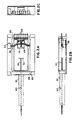
- Figure 1 illustrates a generalized package for an optoelectronic component and a method for assembling the package, according to this invention.
- Package 10 shown partially cut-away in Fig. 1, comprises a housing 12, which completely encloses the necessary components that convert input electrical signals to optical signals.
- housing 12 is made of brass and has a removable top for access to the interior.
- a carrier 14 having a surface that is readily solderable, such as gold-plated copper or brass, is used to support the components.
- a pedestal 16 is secured to a first major surface of carrier 14 adjacent to a first end wall 15 of housing 12, for mounting and positioning a semiconductor laser 22 having a photo-active spot 23.
- Two lateral stops 18 and two axial stops 20 are also secured in a central location to the same major surface of carrier 14 for positioning a lens 24, which is hard soldered prior to the optical fiber alignment.
- carrier 14, pedestal 16 and stops 18, 20 are integrally formed as a one-piece element.
- a thermoelectric cooler 26 is secured to the second major surface of carrier 14.
- a second end wall 28 has a circular opening (not shown in Fig. 1) to permit the insertion of the thick end of uptapered optical fiber 30, which is enclosed in a fiber tube 32 and rigidly held perpendicular to end wall 28 by a large flange 34.
- the lens 24 focuses the light from the photoactive spot 23 of laser 22 onto uptapered optical fiber 30.
- a plurality of mechanical features, and registration features and/or reference marks are incorporated into housing 12 and carrier 14 so that the total package 10 mechanically controls the uptapered-fiber optical tolerances, thus allowing a relaxation of the uptapered optical fiber positional tolerance.
- the uptapered-fiber optical tolerances controlled by package 10 are, the semiconductor position, the lens-to-semiconductor distance; the stability of lens attachment; and the tight angular control of the uptapered fiber.
- a one-piece carrier 14 holds the laser 22 and the lens 24. This controls the stability of the lens-to-semiconductor positional tolerance. Semiconductor 22 and lens 24 move in unison, despite shifts in other package parts caused by vibrations or thermal variations.
- the lens 24 is hard soldered prior to doing the optical fiber alignment to provide mechanical stability. For this optical element, lens 24, stability is more important than exact positioning. Some misalignment of the lens 24 can be compensated for during alignment of the uptapered optical fiber 30.
- the height of pedestal 16 controls the height of laser 22 (y-axis).
- the forward edge 36 of pedestal 16 serves as the forward reference mark for laser 22 (z-axis).
- a lateral reference mark 38 on pedestal 16 is aligned with an active region reference mark 40 on laser 22 (x-axis) to control the lateral position of laser 22.
- Axial stops 20 control the lens-to-semiconductor distance, while lateral stops 18 control the horizontal alignment of the lens 24 to the photo-active spot 23 of laser 22.
- the relative positioning of the laser 22 and the lens 24 is usually set to a positional accuracy of about one-half mil. This can be done off-line under a stereomicroscope, making use of the reference marks 36, 38, 40.
- the position of the lens 24 sets the magnification of the light-emitting area (photo-active spot 23) of laser 22.
- the magnification is set to best match the projected emitting area size with the core of the uptapered optical fiber 30.
- the proper magnification position is set by the axial and lateral stops 18, 20, which are registration features on the carrier 14.
- the uptapered optical fiber 30, protected by a fiber tube holder 32, is mounted and aligned externally to the package 10.
- the uptapered end of optical fiber 30 extends inside the package to a fiber tip reference mark 42 on carrier 14, which is a known distance from axial lens stops 20.
- the package cover (not shown in the figures) is in place, so that the interior of the package is protected from damage.
- the uptapered optical fiber 30 is actively aligned, requiring only crude low cost micro-meters and is secured in position with simple means such as epoxy or screws (not shown in Fig. 1). Active alignment means the fiber is aligned to maximize the light beam entering the fiber while the laser is operating.
- the uptapered optical fiber 30 and the fiber tube holder 32 are easily removed and replaced for packages that have suffered fiber damage, because interior parts need not be disturbed.
- the uptapered optical fiber is held perpendicular to the package by a large fiber flange 34 on the fiber tube holder 32. This controls the angular uptapered optical fiber optical tolerance. It also improves stability because an uptapered optical fiber is more sensitive to angular misalignment than a conventional tapered and lensed or cleaved fiber.
- a long focal distance between the lens 24 and the uptapered end of optical fiber 30 allows space to introduce optical elements such as filters and opto-isolators. In this space the light beam is nearly collimated, greatly simplifying the optical designs incorporating these elements.
- the carrier 14 supporting the lens 24 and semiconductor 22 could be part of a circuit board, multi-chip module, or semiconductor waferboard carrying other optical and electronic components.
- the lens 24 could be either a GRIN type, convex, plano-convex, or combination of several lenses. The only requirement is that it provide the necessary magnification to match light spot sizes with the uptapered end of optical fiber 30.
- Internal optical elements such as opto-isolators or filters, can be located in the space between the lens 24 and the fiber 30 in any combination.
- Optical coatings could also be placed on the lens 24 to provide some of the function of these optical elements.
- the registration or reference marks 18, 20, 36, 38, 42 on the carrier can be either mechanical stops, slots, pins, visual lines, steps or the like. The only requirement is that they be part of the carrier 14 and provide half mil or better accuracy for the lens 24 and the semiconductor 22 positions.
- Fig. 1 shows the uptapered-fiber laser package with the lid removed so that the components are visible.
- This package incorporates an externally aligned uptapered fiber 30, which is aligned and epoxied onto the outside of the package housing 12 at room temperature. This is the only active alignment, and can be performed without piezoelectric staging because of the relaxed lateral alignment tolerances.
- An AR-coated GRIN lens images the laser spot onto the uptapered fiber. This lens is soldered in place with high temperature solder for maximum stability.
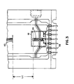
- FIGS. 2a, 2b, 2c, 3 and 4 illustrate details of the preferred embodiment of the uptapered single-mode optical fiber package according to the invention, as built and tested by the inventors.
- the same reference numbers are used for corresponding parts as were used in Fig. 1.
- FIGS 2a, 2b and 2c are top, side and end views of the preferred embodiment of package 10, illustrating its assembly.
- the following items are specific to this embodiment.
- a graduated index (GRIN) lens is used for lens 24.
- a thermo-electric temperature control (TEC) 26 is present.
- This package is designed for epi-down semiconductor mounting.
- the carrier 14 does not extend the full length of the housing 12, so the fiber tip reference mark 42 is on the base of the housing.
- a precision fiber tube 32 having an epoxy fill tube 60 for securing the optical fiber 30 after alignment holds the uptapered end of the optical fiber.
- Fiber tube flange 34 surrounding fiber tube 32 is fastened with epoxy to the outside of the at epoxy joint 62 to complete the alignment.
- a screw mounting slot 50 is present.
- An SMA connector socket 54, a high frequency microline 56 connected thereto, and seven d.c. in-line pin outs to provide high speed electrical signals complete the package.
- the package housing 12, the fiber tube 32, and the cover (not shown) are preferably, made of brass.
- Carrier 14 is preferably made of nickel and gold-plated copper.
- Package 10 in this embodiment is a high speed laser package having the uptapered fiber optical tolerance controls built into the package.
- VPR-BH Vapor-Phase-Regrowth Burled Heterostructure
- the lens 24 used is a SELFOC GRIN lens (model PCH 1.8 - 0.22).
- the uptapered fiber 30 used was made at GTE Laboratories Incorporated. It has an uptapered core size of 90 ⁇ and a single mode fiber core size 9 ⁇ . The fiber has a cut and polished tip to reduce light scattering loss.
- This embodiment uses epi-down lasers. This eliminates the positional tolerance associated with the thickness of the wafer because the light emitting area is essentially at the pedestal/semiconductor interface.
- a reference mark 40 on the laser 22 enables its correct positioning on the pedestal 16 during assembly since the active region 23 in the semiconductor 22 is on the reverse side and not visible.
- the GRIN lens 24 straddles a slot that determines its height above the carrier and its lateral position.
- the back edge of the lens registers with a raised edge on the carrier 14 that defines the axial stop 20.
- Table I compares observed tolerances for the uptapered fiber package with those of a typical lensed-and-tapered fiber package. These tolerances represent the measured misalignment which reduces the coupled power by about 25%.2
- the most important implications of this table for package design are: 1) the relaxed tolerance in the uptapered fiber position (lateral and transverse) is responsible for the increased yield, stability, and ease of assembly, 2) Critical tolerances (angular alignment and magnification) are met by built-in alignment marks and stops in the one-piece carrier, fiber flange, and housing, as schematically shown in Figure 1.
- the fiber flange was designed to automatically align the uptapered fiber parallel to the beam within 0.5°.
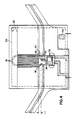
- FIGS 3 and 4 are enlarged top views of the embodiment of Fig. 2a, showing further details of the package features which mechanically control the fiber optic tolerances.
- L1 is the distance between laser 22 and lens 24 while L2 is the distance between lens 24 and uptapered-fiber 50.
- Distance L1 was 15.5 mils.
- a magnification of 10 was used to optically match the semiconductor spot size 23 with the uptapered core.
- Distance L1 can be checked with a low power (30x) stereomicroscope.
- Distance L2 is controlled by setting the fiber tip at the fiber tip reference mark. L2 is 0.475 inches.
- the GRIN lens 24 is soldered to the carrier 16 with a reasonably hard 52/48 In/Sn 118° C solder.
- the solder should be reflowed, and the lens position adjusted along its slot if L1 is found incorrect when checked.
- the fiber tube flange 34 controls the fiber angle at 90°.
- the package normally does not require angular alignment. Only translational alignment is needed.
- Our uptapered fiber 30 requires an angular alignment of one half degree of arc. If the tolerances listed in Table I are maintained, and the L1 position is checked and adjusted properly, the package will achieve this.
- the active alignment process must include angular alignment of the fiber 30 rather than just lateral alignment. This is done by varying the angle of the fiber tube 32 slightly about the horizontal and vertical axes. Epoxy may still be used to join 62 the flange to the package.
- the completed package offers both temperature and optical power monitoring of the semiconductor 22. Temperature regulation is provided by the thermoelectric cooler 26 as controlled by the thermistor 30. Optical power monitoring is provided by the rear facet detector 72 that measures the lost light emitting from the rear of the laser 22.
- a 50 ohm impedance microstrip line transmits the high speed signal between the laser and an SMA microwave connector 54.
- a short wirebond between the semiconductor 22 and microstrip 56 minimizes parasitic capacitances and inductances.
- the microstrip line 56 opposite the SMA connector 54 provides for only mechanical positioning and serves no electrical function.
- a second embodiment (not shown) is the same as the first embodiment except that the semiconductor laser 22 is mounted epi-up. This means that the light emitting region 23 is now near the top surface of the semiconductor die.
- the pedestal height 17 must be reduced to off-set the thickness of the semiconductor 22 and bring the light-emitting spot 23 back to the axis of the lens 24.
- the comparative disadvantage of this design is that the wafer thickness now becomes a controlling optical tolerance requiring an additional wafer thinning processing step or alternatively a set of calibrated carriers with different known pedestal heights.
- the material comprising the package housing 12 may be metal, ceramic or plastic.
- the diameter of the uptapered-fiber 30 may be increased requiring a greater magnification from the lens 24.
- the greater magnification is achieved by using a different lens or lens position. This variation, of increasing the magnification, results in further reduction of the lateral positional tolerance.
- the length of the thick section of the uptapered-fiber 30 may be altered. A shorter length section would make a more compact package.
- the fiber 30 may be held by a variety of different shaped holders but it always needs to be held rigidly. It is likely that it would always require some kind of flange type attachment 34 such as the one in figure 1 to maintain stability.
- the uptapered package may be designed to accommodate the commercial flange rather than have a special package flange.
- the mode of fastening the fiber may be varied. Different types of epoxies, polyesters, solders or welds may be used. In some circumstances it may be possible to screw, crimp, or even use an amalgam to attach the fiber holder to the package.
- the package is made more compact by using stronger, shorter focal length lenses.
- the end of the uptapered-fiber is placed closer to the lens.
Landscapes
- Physics & Mathematics (AREA)
- General Physics & Mathematics (AREA)
- Optics & Photonics (AREA)
- Optical Couplings Of Light Guides (AREA)
- Semiconductor Lasers (AREA)
Applications Claiming Priority (4)
| Application Number | Priority Date | Filing Date | Title |
|---|---|---|---|
| US07/487,497 US5011247A (en) | 1990-03-02 | 1990-03-02 | Uptapered single-mode optical fiber package for optoelectronic components |
| US487497 | 1990-05-21 | ||
| US526367 | 1990-05-21 | ||
| US07/526,367 US5018820A (en) | 1990-03-02 | 1990-05-21 | Method of optically coupling an uptapered single-mode optical fiber to optoelectronic components |
Publications (2)
| Publication Number | Publication Date |
|---|---|
| EP0444610A2 true EP0444610A2 (de) | 1991-09-04 |
| EP0444610A3 EP0444610A3 (en) | 1992-08-12 |
Family
ID=27049023
Family Applications (1)
| Application Number | Title | Priority Date | Filing Date |
|---|---|---|---|
| EP19910102822 Withdrawn EP0444610A3 (en) | 1990-03-02 | 1991-02-26 | Uptapered single-mode optical fiber package for optoelectronic components |
Country Status (4)
| Country | Link |
|---|---|
| US (1) | US5018820A (de) |
| EP (1) | EP0444610A3 (de) |
| JP (1) | JPH0792356A (de) |
| CA (1) | CA2037030A1 (de) |
Cited By (3)
| Publication number | Priority date | Publication date | Assignee | Title |
|---|---|---|---|---|
| EP0533110A1 (de) * | 1991-09-19 | 1993-03-24 | Eastman Kodak Company | Laserdiode mit Kartenrandverbinder |
| US5461692A (en) * | 1993-11-30 | 1995-10-24 | Amoco Corporation | Multimode optical fiber coupling apparatus and method of transmitting laser radiation using same |
| WO1999015928A1 (en) * | 1997-09-19 | 1999-04-01 | Uniphase Telecommunications Products, Inc. | Integrated wavelength-select transmitter |
Families Citing this family (12)
| Publication number | Priority date | Publication date | Assignee | Title |
|---|---|---|---|---|
| GB2242755B (en) * | 1990-03-31 | 1994-07-27 | Plessey Co Ltd | Optical fibre coupling device |
| US5276756A (en) * | 1991-12-06 | 1994-01-04 | Amoco Corporation | High speed electro-optical signal translator |
| US5299272A (en) * | 1993-01-27 | 1994-03-29 | Origin Medststems, Inc. | Method for attaching a gradient index lens to an optical fibre in the course of making an optical instrument |
| US5857047A (en) * | 1996-03-20 | 1999-01-05 | The Regents Of The University Of California | Automated fiber pigtailing machine |
| US6325551B1 (en) | 1999-12-08 | 2001-12-04 | New Focus, Inc. | Method and apparatus for optically aligning optical fibers with optical devices |
| US20030124336A1 (en) * | 2001-11-30 | 2003-07-03 | Keane James M. | Adhesive system for absorbent structures |
| DE102012102306B4 (de) * | 2012-03-19 | 2021-05-12 | OSRAM Opto Semiconductors Gesellschaft mit beschränkter Haftung | Laserdiodenvorrichtung |
| US8867582B2 (en) * | 2012-04-04 | 2014-10-21 | Osram Opto Semiconductors Gmbh | Laser diode assembly |
| US9008138B2 (en) | 2012-04-12 | 2015-04-14 | Osram Opto Semiconductors Gmbh | Laser diode device |
| DE102012103160A1 (de) | 2012-04-12 | 2013-10-17 | Osram Opto Semiconductors Gmbh | Laserdiodenvorrichtung |
| CN103944062A (zh) * | 2014-04-29 | 2014-07-23 | 鞍山创鑫激光技术有限公司 | 一种单芯片光纤耦合输出的半导体激光器 |
| US9869820B2 (en) | 2015-12-09 | 2018-01-16 | Canon U.S.A, Inc. | Optical probe, light intensity detection, imaging method and system |
Family Cites Families (7)
| Publication number | Priority date | Publication date | Assignee | Title |
|---|---|---|---|---|
| NL180882C (nl) * | 1976-05-31 | 1987-05-04 | Philips Nv | Optisch koppelelement en optische koppelinrichting met zulke koppelelementen. |
| US4237474A (en) * | 1978-10-18 | 1980-12-02 | Rca Corporation | Electroluminescent diode and optical fiber assembly |
| US4737004A (en) * | 1985-10-03 | 1988-04-12 | American Telephone And Telegraph Company, At&T Bell Laboratories | Expanded end optical fiber and associated coupling arrangements |
| US4767171A (en) * | 1986-03-27 | 1988-08-30 | Siemens Aktiengesellschaft | Transmission and reception module for a bidirectional communication network |
| EP0259018B1 (de) * | 1986-09-02 | 1991-10-16 | Amp Incorporated | Optoelektronische Verpackungseinheit für einen Halbleiterlaser |
| JPS6365411A (ja) * | 1986-09-08 | 1988-03-24 | Matsushita Electric Ind Co Ltd | レンズ固定方法 |
| JPH073907B2 (ja) * | 1987-07-03 | 1995-01-18 | 株式会社日立製作所 | デュアルインラインパッケ−ジ形半導体レ−ザモジュ−ル |
-
1990
- 1990-05-21 US US07/526,367 patent/US5018820A/en not_active Expired - Lifetime
-
1991
- 1991-02-25 CA CA002037030A patent/CA2037030A1/en not_active Abandoned
- 1991-02-26 EP EP19910102822 patent/EP0444610A3/en not_active Withdrawn
- 1991-02-28 JP JP3055779A patent/JPH0792356A/ja not_active Withdrawn
Cited By (5)
| Publication number | Priority date | Publication date | Assignee | Title |
|---|---|---|---|---|
| EP0533110A1 (de) * | 1991-09-19 | 1993-03-24 | Eastman Kodak Company | Laserdiode mit Kartenrandverbinder |
| US5461692A (en) * | 1993-11-30 | 1995-10-24 | Amoco Corporation | Multimode optical fiber coupling apparatus and method of transmitting laser radiation using same |
| WO1999015928A1 (en) * | 1997-09-19 | 1999-04-01 | Uniphase Telecommunications Products, Inc. | Integrated wavelength-select transmitter |
| US6226424B1 (en) | 1997-09-19 | 2001-05-01 | Uniphase Telecommunications Products, Inc. | Integrated wavelength-select transmitter |
| US6370290B1 (en) | 1997-09-19 | 2002-04-09 | Uniphase Corporation | Integrated wavelength-select transmitter |
Also Published As
| Publication number | Publication date |
|---|---|
| US5018820A (en) | 1991-05-28 |
| CA2037030A1 (en) | 1991-09-03 |
| EP0444610A3 (en) | 1992-08-12 |
| JPH0792356A (ja) | 1995-04-07 |
Similar Documents
| Publication | Publication Date | Title |
|---|---|---|
| US5011247A (en) | Uptapered single-mode optical fiber package for optoelectronic components | |
| KR920010947B1 (ko) | 광결합장치와 그 제조방법, 발광장치와 그 조립방법 및 렌즈홀더 | |
| US5018820A (en) | Method of optically coupling an uptapered single-mode optical fiber to optoelectronic components | |
| US5127072A (en) | Laser module with compliant optical fiber coupling | |
| US4988159A (en) | Fiber tailed optoelectronic transducer | |
| US6374004B1 (en) | Optical subassembly | |
| US6155724A (en) | Light transmitting module for optical communication and light transmitting unit thereof | |
| US5257336A (en) | Optical subassembly with passive optical alignment | |
| US6092935A (en) | Optoelectronic transmitting and/or receiving module and method for its production | |
| JPH04261076A (ja) | 光学素子の製造方法 | |
| JPH03233414A (ja) | 光半導体モジュールの組立方法 | |
| EP0893720A2 (de) | Ein Mikro-Photonikmodul mit einer Trennwand | |
| US6406195B1 (en) | Interface between opto-electronic devices and fibers | |
| JPH1123914A (ja) | 光素子と光ファイバとの固定構造 | |
| US5255333A (en) | Opto-electronic transducer arrangement having a lens-type optical coupling | |
| US5024504A (en) | Method of aligning and packaging an optoelectronic component with a single-mode optical fiber array | |
| US6955480B2 (en) | Actively aligned optoelectronic device | |
| JPH07199006A (ja) | 光サブアセンブリ及び光モジュール | |
| EP0570891B1 (de) | Linsenhalterung für Halbleiterlaser | |
| JP3022724B2 (ja) | 光半導体モジュール | |
| US6643420B2 (en) | Optical subassembly | |
| US4957342A (en) | Single-mode optical fiber array package for optoelectronic components | |
| US20040161208A1 (en) | Low cost optical module | |
| Yamauchi et al. | Automated mass production line for optical module using passive alignment technique | |
| JP2003520353A (ja) | マルチファイバアレー用光電子モジュール |
Legal Events
| Date | Code | Title | Description |
|---|---|---|---|
| PUAI | Public reference made under article 153(3) epc to a published international application that has entered the european phase |
Free format text: ORIGINAL CODE: 0009012 |
|
| AK | Designated contracting states |
Kind code of ref document: A2 Designated state(s): DE FR GB NL |
|
| PUAL | Search report despatched |
Free format text: ORIGINAL CODE: 0009013 |
|
| AK | Designated contracting states |
Kind code of ref document: A3 Designated state(s): DE FR GB NL |
|
| STAA | Information on the status of an ep patent application or granted ep patent |
Free format text: STATUS: THE APPLICATION IS DEEMED TO BE WITHDRAWN |
|
| 18D | Application deemed to be withdrawn |
Effective date: 19930213 |