EP0443668A2 - Frequenzumsetzer mit Beseitigung der Spiegelfrequenz in planarer Technologie - Google Patents
Frequenzumsetzer mit Beseitigung der Spiegelfrequenz in planarer Technologie Download PDFInfo
- Publication number
- EP0443668A2 EP0443668A2 EP91200312A EP91200312A EP0443668A2 EP 0443668 A2 EP0443668 A2 EP 0443668A2 EP 91200312 A EP91200312 A EP 91200312A EP 91200312 A EP91200312 A EP 91200312A EP 0443668 A2 EP0443668 A2 EP 0443668A2
- Authority
- EP
- European Patent Office
- Prior art keywords
- lines
- image rejection
- section
- port
- converter
- Prior art date
- Legal status (The legal status is an assumption and is not a legal conclusion. Google has not performed a legal analysis and makes no representation as to the accuracy of the status listed.)
- Granted
Links
Images
Classifications
-
- H—ELECTRICITY
- H03—ELECTRONIC CIRCUITRY
- H03D—DEMODULATION OR TRANSFERENCE OF MODULATION FROM ONE CARRIER TO ANOTHER
- H03D9/00—Demodulation or transference of modulation of modulated electromagnetic waves
- H03D9/06—Transference of modulation using distributed inductance and capacitance
- H03D9/0608—Transference of modulation using distributed inductance and capacitance by means of diodes
- H03D9/0633—Transference of modulation using distributed inductance and capacitance by means of diodes mounted on a stripline circuit
- H03D9/0641—Transference of modulation using distributed inductance and capacitance by means of diodes mounted on a stripline circuit located in a hollow waveguide
-
- H—ELECTRICITY
- H03—ELECTRONIC CIRCUITRY
- H03D—DEMODULATION OR TRANSFERENCE OF MODULATION FROM ONE CARRIER TO ANOTHER
- H03D7/00—Transference of modulation from one carrier to another, e.g. frequency-changing
- H03D7/14—Balanced arrangements
- H03D7/1408—Balanced arrangements with diodes
-
- H—ELECTRICITY
- H03—ELECTRONIC CIRCUITRY
- H03D—DEMODULATION OR TRANSFERENCE OF MODULATION FROM ONE CARRIER TO ANOTHER
- H03D2200/00—Indexing scheme relating to details of demodulation or transference of modulation from one carrier to another covered by H03D
- H03D2200/0001—Circuit elements of demodulators
- H03D2200/0011—Diodes
- H03D2200/0013—Diodes connected in a ring configuration
-
- H—ELECTRICITY
- H03—ELECTRONIC CIRCUITRY
- H03D—DEMODULATION OR TRANSFERENCE OF MODULATION FROM ONE CARRIER TO ANOTHER
- H03D7/00—Transference of modulation from one carrier to another, e.g. frequency-changing
- H03D7/16—Multiple-frequency-changing
-
- H—ELECTRICITY
- H03—ELECTRONIC CIRCUITRY
- H03D—DEMODULATION OR TRANSFERENCE OF MODULATION FROM ONE CARRIER TO ANOTHER
- H03D7/00—Transference of modulation from one carrier to another, e.g. frequency-changing
- H03D7/18—Modifications of frequency-changers for eliminating image frequencies
-
- H—ELECTRICITY
- H03—ELECTRONIC CIRCUITRY
- H03D—DEMODULATION OR TRANSFERENCE OF MODULATION FROM ONE CARRIER TO ANOTHER
- H03D9/00—Demodulation or transference of modulation of modulated electromagnetic waves
- H03D9/06—Transference of modulation using distributed inductance and capacitance
- H03D9/0608—Transference of modulation using distributed inductance and capacitance by means of diodes
- H03D9/0633—Transference of modulation using distributed inductance and capacitance by means of diodes mounted on a stripline circuit
Definitions
- the present invention relates to the field of frequency conversion and more specifically to an image rejection frequency converter in planar technology operating in the microwave range.
- Frequency converters of the general type are employed as is known in transmitters and receivers of radiofrequency signals for the main purpose of translating the entire band of modulated signals to a frequency better suited to transmission or reception.
- the converters mentioned above belong to a first type of converter termed 'double side band'.
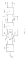
- FIG. 1 The most general circuit configuration used in image rejection converters of the known type is shown in FIG. 1. It comprises:
- the power divider DIV is a balun because it converts the unbalanced signal LO into two signals balanced with the ground potential, coupling them to the ports 1P1 and 1P2.
- a known variant on the above mentioned circuit configuration provides for the use of merely balanced mixers which require two duplexer filters which allow coupling of the radiofrequency signals RF and intermediate frequency signals BLS or BLI to a single port of the respective mixers MIX1, MIX2.
- FIG. 1 can be embodied either with mechanical wave guide technology or with the more modern thin film planar technology. In both cases to obtain converters having good operating characteristics special care in designing the baluns is essential.
- the state of the art includes different examples of image rejection converters provided in planar technology operating in the microwave range, each having its own original embodiment of the balun.
- a first converter structure is described in the article entitled “Single side band mixers for communications systems” by Ben R. Hallford and published in IEEE MTT-S DIGEST in 1982.
- the main drawback of the converter described is that it has a narrow operating band.
- the structure is cumbersome, especially in the embodiment operating at the lowest frequencies allowed by the technology employed.
- the structure of the converter is specifically aimed at suppression of the harmonics of the local oscillator and, in this case also, is cumbersome.
- the object of the present invention is to overcome the above drawbacks and indicate an image rejection frequency converter provided in planar technology comprising essentially an integrated power divider with a balun which couples a local oscillator signal to the ends of two frequency mixers having ports to which arrive, or from which leave, radiofrequency signals and intermediate frequency signals.
- the converter possesses a characteristic configuration provided in microstrip and in coplanar line which allows the power divider to convert a local oscillator signal not balanced with ground potential into a balanced signal for coupling to the ends of the mixers, preventing their appearing at the ports of the mixers affected by the radiofrequency and intermediate frequency signals.
- the object of the present invention is an image rejection frequency converter provided in planar technology as described in claim 1.
- the structure of the converter which is the object of the invention is more compact and has several advantages.
- a first advantage is that it can be used even with relatively low frequencies on the order of 500MHz to 1GHz.
- a second advantage is that it makes possible achieving a large pass band which with special construction arrangements can be extended to three octaves.
- a third advantage is its construction simplicity.
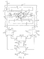
- FIG. 2 shows an overall view of the image rejection converter which is the object of the present invention.
- the view includes a circuit part and four function blocks connected together and to said circuit part.
- reference number 1 indicates an insulating substrate, e.g. alumina, having on the upper face an extended metallization 2.
- the metallization 2 acts as a ground plane and leaves uncovered three zones of the substrate 1 rectangular in form and indicated by numbers 3, 4, and 5. Said rectangular zones have the same length and are aligned one under the other.
- the central zone 4 is at exactly one half the distance in relation to the outer zones 3 and 5.
- the central zone 4 on the same face of the ground plane 2 includes two metallized lines 8 and 9 parallel to the lines 6 and 7.
- the lines 8 and 9 cover almost entirely the zone without metallization 4 except for a small central portion.
- the outer end of the lines 8 and 9 included two metallized holes indicated respectively by 10 and 11.
- the pair of diodes D1 and D2 forms a first mixer MIX1.
- the pair of diodes D3 and D4 forms a second mixer MIX2.
- the diode D1 has its anode connected to the line 6 at point 6' and the cathode connected to the line 8 at point 8'.
- the diode D2 has the anode connected to the line 8 at point 8' and the cathode connected to the line 7 at point 7'.
- the diode D3 has the cathode connected to the line 6 at point 6' and the anode connected to the line 9 at point 9'.
- the diode D4 has its cathode connected to the line 9 at point 9' and the anode connected to the line 7 at point 7'.
- the face of the substrate 1 opposite that of the ground plane 2 includes three metallization lines indicated by M1, M2 and M3 which, together with the ground plane 2, form three microstrip lines.
- the microstrip line M1 is composed of four contiguous line sections indicated by 12, 13, 14 and 15.
- the first section 12 has one end connected to a terminal T1 to which arrives the local oscillator signal LO. The other end is connected to the horizontal line section 13.
- the section 13 is placed in correspondence with the line 6 and extends half the length thereof and continues in the vertical section 14 located adjacent to the central portion of the rectangular zone 4.
- the line section 14 is connected to the horizontal line section 15.
- the section 15 is placed opposite the line 7 and extends in the same direction as the section 13 for a length slightly less than that of said section 13.
- the microstrip line M2 connects through the metallized hole 10 the line 8 to a terminal T2.
- the microstrip line M3 connects through the metallized hole 11 the line 9 to a terminal T3.
- the terminal T2 is connected to a first port 16 of a first duplexer filter FD1 formed of a low-pass section FPB1 and a high-pass section FPA1.
- the high-pass section FPA1 is connected to the port 16 and to a second port 18 while the low-pass section is connected to the port 16 and to a third port 17.
- the terminal T3 is connected to a first port 19 of a second duplexer filter FD2 identical to the first one and formed of a low-pass section FPB2 and a high-pass section FPA2.
- the high-pass section FPA2 is connected to the port 19 and to a second port 21, the low-pass section is connected to the port 19 and to a third port 20.
- duplexer filters FD1 and FD2 are provided in accordance with known techniques which use concentrated or distributed elements.
- the converter of FIG. 2 includes the in quadrature hybrid circuits HYB-RF and HYB-IF, operating on radiofrequency and intermediate frequency respectively.
- Said hybrid circuits are of known type. They have four ports indicated by 22, 23, 24, 25 and 26, 27, 28, 29 respectively.
- the adjacent port 23 is closed on a termination TERM connected to ground.
- the ports 24 and 25 of HYB-RF are connected to the second ports 18 and 21 of the filters FD1 and FD2 belonging to the high-pass sections FPA1 and FPA2.
- the intermediate frequency signals BLI and BLS are present at the ports 28 and 29 of HYB-IF.
- the double arrow indicates that the signals can be incoming or outgoing depending on the fact that the converter is used for transmission or reception.
- the ports 26 and 27 of the intermediate frequency hybrid HYB-IF are connected to the third ports of the filters FD1 and FD2 which correspond to the low-pass sections FPB1 and FPB2.
- the two mixers MIX1 and MIX2 are supplied by the local oscillator signal LO by means of the microstrip line M1. Therefore the signal LO input at the terminal T1 is not balanced with the ground potential.
- the sections 13, 14 and 15 of M1 associated with the lines 6 and 7 function as baluns for the signal LO.
- the structure shown in FIG. 2 possesses the following characteristics.
- radiofrequency signals RF and intermediate frequency signals BLS and/or BLI reach or come from the mixers MIX1 and MIX2 through the microstrips M2, M3 and the coplanar lines formed by the lines 8 and 9 with the lines 6 and 7.
- the transition from microstrip to coplanar takes place for said signals through the metallized holes 10 and 11.
- the width of the lines 8 and 9 and their distance from the lines 6 and 7 are such as to achieve a characteristic impedance for said coplanar lines identical to that (50 ohm) of the microstrips M2 and M3.
- the signal RF received is divided by the hybrid HYB-RF in two radiofrequency signals mutually phase shifted 90°. Said signals pass through the high-pass sections of the duplexer filters FD1 and FD2 to reach in the manner indicated above the mixers MIX1 and MIX2. More specifically, between the points 8' and 6' and between the points 8' and 7' of the mixer MIX1, there is a first radiofrequency signal. Between the points 9' and 6' and between the points 9' and 7' of MIX2 there is the second radiofrequency signal.
- the local oscillator signal LO sends alternately in conduction the pair of diodes D1, D2 and D3, D4 which generate a first and a second intermediate frequency beat signal.
- Said intermediate frequency signals travel backward over the same path travelled by the radiofrequency signals, reach the terminals T2 and T3, then pass through the low-pass section of the filters FD1 and FD2 and reach the ports 26 and 27 of the hybrid HYB-IF.
- the latter recombines the above intermediate frequency signals which are in quadrature obtaining at the ports 28 and 29 the signals BLI and BLS which, as mentioned, correspond to the conversion to intermediate frequency of the lower and upper side bands respectively of the RF signal.
- duplexer filters FD1 and FD2 actuate the separation of the radiofrequency signals RF and intermediate frequency signals BLS and/or BLI which are simultaneously present at the terminals T2 and T3.
- the points 6' and 7' identify an application port of the signal LO common to the two mixers MIX1 and MIX2.
- the points 8' and 6', 7' considered together identify a first port of the mixer MIX1 to which arrive, or from which depart, the first radiofrequency signals and intermediate frequency signals.
- the points 9' and 6', 7' considered together identify a second port of the mixer MIX2 to which arrive, or from which depart, the second radiofrequency signals and intermediate frequency signals.
- the ports of the converters are the following:
- the terminal T1 represents the input port of the local oscillator signal LO.
- the port 22 of HYB-RF is the radiofrequency port for the signal RF.
- the ports 28 and 29 of HYB-IF are the intermediate frequency ports for the signals BLI and BLS.
- the structure of the converter which is the object of the invention allows optimal insulation between the local oscillator port and the radiofrequency port.
- the RF signal is not propagated toward he terminal T1 because the balun allows propagation toward T1 of the radiofrequency signals only if they are in phase opposition at points 6' and 7'. As mentioned above the points 6' and 7' are equipotential for the radiofrequency signals.
- the local oscillator signal LO present at the terminal T1 does not appear on the microstrips M2 and M3 and hence at the radiofrequency port 22.
- the structure of the converter possesses the advantage, particularly useful in transmission, of avoiding costly filters capable of attenuating the local oscillator signal.
- planar structure allows integration on a single substrate 1 even of the duplexer filters FD1, FD2 and of the hybrid circuits HYB-RF, HYB-IF, providing a smaller and highly functional converter.
Landscapes
- Engineering & Computer Science (AREA)
- Power Engineering (AREA)
- Physics & Mathematics (AREA)
- Electromagnetism (AREA)
- Input Circuits Of Receivers And Coupling Of Receivers And Audio Equipment (AREA)
- Superheterodyne Receivers (AREA)
- Glass Compositions (AREA)
- Apparatus For Radiation Diagnosis (AREA)
- Arc Welding In General (AREA)
Applications Claiming Priority (2)
| Application Number | Priority Date | Filing Date | Title |
|---|---|---|---|
| IT1943390 | 1990-02-21 | ||
| IT19433A IT1239637B (it) | 1990-02-21 | 1990-02-21 | Convertitore di frequenza a reiezione d'immagine realizzato in tecnologia planare |
Publications (3)
| Publication Number | Publication Date |
|---|---|
| EP0443668A2 true EP0443668A2 (de) | 1991-08-28 |
| EP0443668A3 EP0443668A3 (en) | 1991-11-13 |
| EP0443668B1 EP0443668B1 (de) | 1994-06-22 |
Family
ID=11157902
Family Applications (1)
| Application Number | Title | Priority Date | Filing Date |
|---|---|---|---|
| EP91200312A Expired - Lifetime EP0443668B1 (de) | 1990-02-21 | 1991-02-14 | Frequenzumsetzer mit Beseitigung der Spiegelfrequenz in planarer Technologie |
Country Status (7)
| Country | Link |
|---|---|
| EP (1) | EP0443668B1 (de) |
| AU (1) | AU634348B2 (de) |
| DE (1) | DE69102557T2 (de) |
| ES (1) | ES2055957T3 (de) |
| IT (1) | IT1239637B (de) |
| NO (1) | NO176858C (de) |
| ZA (1) | ZA911284B (de) |
Cited By (3)
| Publication number | Priority date | Publication date | Assignee | Title |
|---|---|---|---|---|
| US6374093B1 (en) | 1993-11-01 | 2002-04-16 | Nokia Mobile Phones Ltd. | Shifting of frequency range and bandwidth of receivers using a mixer attenuating the image frequency |
| GB2481147A (en) * | 2009-02-25 | 2011-12-14 | Cxr Ltd | X-ray scanners |
| US20130187474A1 (en) * | 2008-07-02 | 2013-07-25 | Access Business Group International Llc | Electromagnetic interference mitigation |
Family Cites Families (4)
| Publication number | Priority date | Publication date | Assignee | Title |
|---|---|---|---|---|
| FR2515449B1 (fr) * | 1981-10-23 | 1986-08-14 | Thomson Csf | Dispositif melangeur subharmonique hyperfrequence et systeme hyperfrequence utilisant un tel dispositif |
| US4607394A (en) * | 1985-03-04 | 1986-08-19 | General Electric Company | Single balanced planar mixer |
| FR2608324B1 (fr) * | 1986-12-11 | 1989-03-24 | Alcatel Espace | Dispositif melangeur doublement equilibre |
| EP0329077B1 (de) * | 1988-02-17 | 1994-08-17 | Siemens Aktiengesellschaft | Einseitenbandmischer in Microstriptechnik |
-
1990
- 1990-02-21 IT IT19433A patent/IT1239637B/it active IP Right Grant
-
1991
- 1991-02-14 EP EP91200312A patent/EP0443668B1/de not_active Expired - Lifetime
- 1991-02-14 DE DE69102557T patent/DE69102557T2/de not_active Expired - Fee Related
- 1991-02-14 ES ES91200312T patent/ES2055957T3/es not_active Expired - Lifetime
- 1991-02-20 NO NO910682A patent/NO176858C/no not_active IP Right Cessation
- 1991-02-20 AU AU71216/91A patent/AU634348B2/en not_active Ceased
- 1991-02-21 ZA ZA911284A patent/ZA911284B/xx unknown
Cited By (4)
| Publication number | Priority date | Publication date | Assignee | Title |
|---|---|---|---|---|
| US6374093B1 (en) | 1993-11-01 | 2002-04-16 | Nokia Mobile Phones Ltd. | Shifting of frequency range and bandwidth of receivers using a mixer attenuating the image frequency |
| US20130187474A1 (en) * | 2008-07-02 | 2013-07-25 | Access Business Group International Llc | Electromagnetic interference mitigation |
| US8952572B2 (en) * | 2008-07-02 | 2015-02-10 | Access Business Group International Llc | Electromagnetic interference mitigation |
| GB2481147A (en) * | 2009-02-25 | 2011-12-14 | Cxr Ltd | X-ray scanners |
Also Published As
| Publication number | Publication date |
|---|---|
| NO910682D0 (no) | 1991-02-20 |
| IT9019433A0 (it) | 1990-02-21 |
| DE69102557T2 (de) | 1995-01-26 |
| DE69102557D1 (de) | 1994-07-28 |
| AU634348B2 (en) | 1993-02-18 |
| EP0443668B1 (de) | 1994-06-22 |
| NO176858B (no) | 1995-02-27 |
| EP0443668A3 (en) | 1991-11-13 |
| AU7121691A (en) | 1991-08-22 |
| ZA911284B (en) | 1991-11-27 |
| NO910682L (no) | 1991-08-22 |
| IT9019433A1 (it) | 1991-08-22 |
| NO176858C (no) | 1995-06-07 |
| IT1239637B (it) | 1993-11-11 |
| ES2055957T3 (es) | 1994-09-01 |
Similar Documents
| Publication | Publication Date | Title |
|---|---|---|
| US4607394A (en) | Single balanced planar mixer | |
| US6094570A (en) | Double-balanced monolithic microwave integrated circuit mixer | |
| CN113131870A (zh) | 对频率进行混频或倍频的装置 | |
| US4662000A (en) | Frequency conversion circuits | |
| EP0322612B1 (de) | Die Spiegelfrequenz herabsetzender harmonischer Mikrowellen-Frequenzumsetzer | |
| US6950631B2 (en) | Active receiving array antenna | |
| US5740528A (en) | Planar triply-balanced microstrip mixer | |
| CA1077145A (en) | Coaxial balun with doubly balanced heterodyne converter | |
| US5428838A (en) | Diode mixer implemented in a planar monolithic IC | |
| US4651344A (en) | VHF-UHF mixer having a balun | |
| EP0443668B1 (de) | Frequenzumsetzer mit Beseitigung der Spiegelfrequenz in planarer Technologie | |
| US3584306A (en) | High frequency converter | |
| JPH03188702A (ja) | マトリックス構造ミクサー | |
| KR100471049B1 (ko) | 링 하이브리드 결합기를 이용한 비방사 유전체 도파관혼합기 | |
| CN113131871A (zh) | 对频率进行混频或倍频的装置 | |
| US4392251A (en) | Symmetric microwave mixer with coplanar diode connection | |
| US4380831A (en) | Symmetric microwave mixer with improved isolation | |
| US4399562A (en) | Full balun mixer | |
| Mourant et al. | A broadband planar image reject mixer | |
| JPS6361501A (ja) | 周波数コンバ−タ一体型平面アンテナ | |
| GB2023954A (en) | A signal mixer | |
| CN113708026B (zh) | 基于缝隙线的差分90度谢夫曼移相器 | |
| EP0389025B1 (de) | Mikrowellen-Frequenzumsetzer | |
| JP2927103B2 (ja) | 高調波ミクサ | |
| Hallford | Simple Balun-Coupled Mixers |
Legal Events
| Date | Code | Title | Description |
|---|---|---|---|
| PUAI | Public reference made under article 153(3) epc to a published international application that has entered the european phase |
Free format text: ORIGINAL CODE: 0009012 |
|
| AK | Designated contracting states |
Kind code of ref document: A2 Designated state(s): CH DE ES FR GB GR IT LI SE |
|
| PUAL | Search report despatched |
Free format text: ORIGINAL CODE: 0009013 |
|
| AK | Designated contracting states |
Kind code of ref document: A3 Designated state(s): CH DE ES FR GB GR IT LI SE |
|
| 17P | Request for examination filed |
Effective date: 19920414 |
|
| 17Q | First examination report despatched |
Effective date: 19931105 |
|
| GRAA | (expected) grant |
Free format text: ORIGINAL CODE: 0009210 |
|
| ITF | It: translation for a ep patent filed | ||
| AK | Designated contracting states |
Kind code of ref document: B1 Designated state(s): CH DE ES FR GB GR IT LI SE |
|
| REF | Corresponds to: |
Ref document number: 69102557 Country of ref document: DE Date of ref document: 19940728 |
|
| REG | Reference to a national code |
Ref country code: GR Ref legal event code: FG4A Free format text: 3012333 |
|
| REG | Reference to a national code |
Ref country code: ES Ref legal event code: FG2A Ref document number: 2055957 Country of ref document: ES Kind code of ref document: T3 |
|
| ET | Fr: translation filed | ||
| EAL | Se: european patent in force in sweden |
Ref document number: 91200312.6 |
|
| PLBE | No opposition filed within time limit |
Free format text: ORIGINAL CODE: 0009261 |
|
| STAA | Information on the status of an ep patent application or granted ep patent |
Free format text: STATUS: NO OPPOSITION FILED WITHIN TIME LIMIT |
|
| 26N | No opposition filed | ||
| PGFP | Annual fee paid to national office [announced via postgrant information from national office to epo] |
Ref country code: CH Payment date: 19970522 Year of fee payment: 7 |
|
| PGFP | Annual fee paid to national office [announced via postgrant information from national office to epo] |
Ref country code: GB Payment date: 19980113 Year of fee payment: 8 |
|
| PGFP | Annual fee paid to national office [announced via postgrant information from national office to epo] |
Ref country code: GR Payment date: 19980130 Year of fee payment: 8 |
|
| PGFP | Annual fee paid to national office [announced via postgrant information from national office to epo] |
Ref country code: ES Payment date: 19980211 Year of fee payment: 8 |
|
| PG25 | Lapsed in a contracting state [announced via postgrant information from national office to epo] |
Ref country code: LI Free format text: LAPSE BECAUSE OF NON-PAYMENT OF DUE FEES Effective date: 19980228 Ref country code: CH Free format text: LAPSE BECAUSE OF NON-PAYMENT OF DUE FEES Effective date: 19980228 |
|
| REG | Reference to a national code |
Ref country code: CH Ref legal event code: PL |
|
| PG25 | Lapsed in a contracting state [announced via postgrant information from national office to epo] |
Ref country code: GB Free format text: LAPSE BECAUSE OF NON-PAYMENT OF DUE FEES Effective date: 19990214 |
|
| PG25 | Lapsed in a contracting state [announced via postgrant information from national office to epo] |
Ref country code: ES Free format text: LAPSE BECAUSE OF NON-PAYMENT OF DUE FEES Effective date: 19990215 |
|
| PG25 | Lapsed in a contracting state [announced via postgrant information from national office to epo] |
Ref country code: GR Free format text: LAPSE BECAUSE OF NON-PAYMENT OF DUE FEES Effective date: 19990228 |
|
| GBPC | Gb: european patent ceased through non-payment of renewal fee |
Effective date: 19990214 |
|
| REG | Reference to a national code |
Ref country code: ES Ref legal event code: FD2A Effective date: 20010503 |
|
| PGFP | Annual fee paid to national office [announced via postgrant information from national office to epo] |
Ref country code: FR Payment date: 20020212 Year of fee payment: 12 |
|
| PGFP | Annual fee paid to national office [announced via postgrant information from national office to epo] |
Ref country code: DE Payment date: 20020227 Year of fee payment: 12 |
|
| PGFP | Annual fee paid to national office [announced via postgrant information from national office to epo] |
Ref country code: SE Payment date: 20030219 Year of fee payment: 13 |
|
| PG25 | Lapsed in a contracting state [announced via postgrant information from national office to epo] |
Ref country code: DE Free format text: LAPSE BECAUSE OF NON-PAYMENT OF DUE FEES Effective date: 20030902 |
|
| PG25 | Lapsed in a contracting state [announced via postgrant information from national office to epo] |
Ref country code: FR Free format text: LAPSE BECAUSE OF NON-PAYMENT OF DUE FEES Effective date: 20031031 |
|
| REG | Reference to a national code |
Ref country code: FR Ref legal event code: ST |
|
| PG25 | Lapsed in a contracting state [announced via postgrant information from national office to epo] |
Ref country code: SE Free format text: LAPSE BECAUSE OF NON-PAYMENT OF DUE FEES Effective date: 20040215 |
|
| EUG | Se: european patent has lapsed | ||
| PG25 | Lapsed in a contracting state [announced via postgrant information from national office to epo] |
Ref country code: IT Free format text: LAPSE BECAUSE OF NON-PAYMENT OF DUE FEES;WARNING: LAPSES OF ITALIAN PATENTS WITH EFFECTIVE DATE BEFORE 2007 MAY HAVE OCCURRED AT ANY TIME BEFORE 2007. THE CORRECT EFFECTIVE DATE MAY BE DIFFERENT FROM THE ONE RECORDED. Effective date: 20050214 |