EP0442561A1 - Semiconductor relay circuit - Google Patents
Semiconductor relay circuit Download PDFInfo
- Publication number
- EP0442561A1 EP0442561A1 EP91200228A EP91200228A EP0442561A1 EP 0442561 A1 EP0442561 A1 EP 0442561A1 EP 91200228 A EP91200228 A EP 91200228A EP 91200228 A EP91200228 A EP 91200228A EP 0442561 A1 EP0442561 A1 EP 0442561A1
- Authority
- EP
- European Patent Office
- Prior art keywords
- mos fet
- gate
- photovoltaic
- source electrodes
- resistor
- Prior art date
- Legal status (The legal status is an assumption and is not a legal conclusion. Google has not performed a legal analysis and makes no representation as to the accuracy of the status listed.)
- Granted
Links
- 239000004065 semiconductor Substances 0.000 title claims abstract description 35
- 230000008034 disappearance Effects 0.000 claims abstract description 3
- 239000000758 substrate Substances 0.000 claims description 3
- 230000004044 response Effects 0.000 description 26
- 238000010586 diagram Methods 0.000 description 7
- 239000000470 constituent Substances 0.000 description 4
- 230000002035 prolonged effect Effects 0.000 description 4
- 230000000630 rising effect Effects 0.000 description 4
- 229920006395 saturated elastomer Polymers 0.000 description 3
- XAGFODPZIPBFFR-UHFFFAOYSA-N aluminium Chemical compound [Al] XAGFODPZIPBFFR-UHFFFAOYSA-N 0.000 description 2
- 229910052782 aluminium Inorganic materials 0.000 description 2
- 238000009792 diffusion process Methods 0.000 description 2
- 150000002500 ions Chemical class 0.000 description 2
- 239000007787 solid Substances 0.000 description 2
- VYPSYNLAJGMNEJ-UHFFFAOYSA-N Silicium dioxide Chemical compound O=[Si]=O VYPSYNLAJGMNEJ-UHFFFAOYSA-N 0.000 description 1
- 230000004075 alteration Effects 0.000 description 1
- 239000003990 capacitor Substances 0.000 description 1
- 230000003247 decreasing effect Effects 0.000 description 1
- 230000005669 field effect Effects 0.000 description 1
- 239000012535 impurity Substances 0.000 description 1
- 230000001939 inductive effect Effects 0.000 description 1
- 230000007257 malfunction Effects 0.000 description 1
- 238000004519 manufacturing process Methods 0.000 description 1
- 230000004048 modification Effects 0.000 description 1
- 238000012986 modification Methods 0.000 description 1
- 230000003071 parasitic effect Effects 0.000 description 1
- 229910052814 silicon oxide Inorganic materials 0.000 description 1
Images

Classifications
-
- H—ELECTRICITY
- H03—ELECTRONIC CIRCUITRY
- H03K—PULSE TECHNIQUE
- H03K17/00—Electronic switching or gating, i.e. not by contact-making and –breaking
- H03K17/51—Electronic switching or gating, i.e. not by contact-making and –breaking characterised by the components used
- H03K17/56—Electronic switching or gating, i.e. not by contact-making and –breaking characterised by the components used by the use, as active elements, of semiconductor devices
-
- H—ELECTRICITY
- H03—ELECTRONIC CIRCUITRY
- H03K—PULSE TECHNIQUE
- H03K17/00—Electronic switching or gating, i.e. not by contact-making and –breaking
- H03K17/51—Electronic switching or gating, i.e. not by contact-making and –breaking characterised by the components used
- H03K17/78—Electronic switching or gating, i.e. not by contact-making and –breaking characterised by the components used using opto-electronic devices, i.e. light-emitting and photoelectric devices electrically- or optically-coupled
- H03K17/785—Electronic switching or gating, i.e. not by contact-making and –breaking characterised by the components used using opto-electronic devices, i.e. light-emitting and photoelectric devices electrically- or optically-coupled controlling field-effect transistor switches
-
- H—ELECTRICITY
- H01—ELECTRIC ELEMENTS
- H01L—SEMICONDUCTOR DEVICES NOT COVERED BY CLASS H10
- H01L31/00—Semiconductor devices sensitive to infrared radiation, light, electromagnetic radiation of shorter wavelength or corpuscular radiation and specially adapted either for the conversion of the energy of such radiation into electrical energy or for the control of electrical energy by such radiation; Processes or apparatus specially adapted for the manufacture or treatment thereof or of parts thereof; Details thereof
- H01L31/12—Semiconductor devices sensitive to infrared radiation, light, electromagnetic radiation of shorter wavelength or corpuscular radiation and specially adapted either for the conversion of the energy of such radiation into electrical energy or for the control of electrical energy by such radiation; Processes or apparatus specially adapted for the manufacture or treatment thereof or of parts thereof; Details thereof structurally associated with, e.g. formed in or on a common substrate with, one or more electric light sources, e.g. electroluminescent light sources, and electrically or optically coupled thereto
- H01L31/16—Semiconductor devices sensitive to infrared radiation, light, electromagnetic radiation of shorter wavelength or corpuscular radiation and specially adapted either for the conversion of the energy of such radiation into electrical energy or for the control of electrical energy by such radiation; Processes or apparatus specially adapted for the manufacture or treatment thereof or of parts thereof; Details thereof structurally associated with, e.g. formed in or on a common substrate with, one or more electric light sources, e.g. electroluminescent light sources, and electrically or optically coupled thereto the semiconductor device sensitive to radiation being controlled by the light source or sources
- H01L31/167—Semiconductor devices sensitive to infrared radiation, light, electromagnetic radiation of shorter wavelength or corpuscular radiation and specially adapted either for the conversion of the energy of such radiation into electrical energy or for the control of electrical energy by such radiation; Processes or apparatus specially adapted for the manufacture or treatment thereof or of parts thereof; Details thereof structurally associated with, e.g. formed in or on a common substrate with, one or more electric light sources, e.g. electroluminescent light sources, and electrically or optically coupled thereto the semiconductor device sensitive to radiation being controlled by the light source or sources the light sources and the devices sensitive to radiation all being semiconductor devices characterised by potential barriers
- H01L31/173—Semiconductor devices sensitive to infrared radiation, light, electromagnetic radiation of shorter wavelength or corpuscular radiation and specially adapted either for the conversion of the energy of such radiation into electrical energy or for the control of electrical energy by such radiation; Processes or apparatus specially adapted for the manufacture or treatment thereof or of parts thereof; Details thereof structurally associated with, e.g. formed in or on a common substrate with, one or more electric light sources, e.g. electroluminescent light sources, and electrically or optically coupled thereto the semiconductor device sensitive to radiation being controlled by the light source or sources the light sources and the devices sensitive to radiation all being semiconductor devices characterised by potential barriers formed in, or on, a common substrate
-
- H—ELECTRICITY
- H03—ELECTRONIC CIRCUITRY
- H03K—PULSE TECHNIQUE
- H03K17/00—Electronic switching or gating, i.e. not by contact-making and –breaking
- H03K17/51—Electronic switching or gating, i.e. not by contact-making and –breaking characterised by the components used
- H03K17/56—Electronic switching or gating, i.e. not by contact-making and –breaking characterised by the components used by the use, as active elements, of semiconductor devices
- H03K17/687—Electronic switching or gating, i.e. not by contact-making and –breaking characterised by the components used by the use, as active elements, of semiconductor devices the devices being field-effect transistors
-
- Y—GENERAL TAGGING OF NEW TECHNOLOGICAL DEVELOPMENTS; GENERAL TAGGING OF CROSS-SECTIONAL TECHNOLOGIES SPANNING OVER SEVERAL SECTIONS OF THE IPC; TECHNICAL SUBJECTS COVERED BY FORMER USPC CROSS-REFERENCE ART COLLECTIONS [XRACs] AND DIGESTS
- Y10—TECHNICAL SUBJECTS COVERED BY FORMER USPC
- Y10S—TECHNICAL SUBJECTS COVERED BY FORMER USPC CROSS-REFERENCE ART COLLECTIONS [XRACs] AND DIGESTS
- Y10S136/00—Batteries: thermoelectric and photoelectric
- Y10S136/291—Applications
- Y10S136/293—Circuits
Definitions
- This invention relates to semiconductor relay circuits and, more particularly, to the semiconductor relay circuit in which a light-emitting diode converts an input signal to a light signal, a photovoltaic diode array optically coupled to the light-emitting diode converts the light signal to an electrical signal which is used for driving a metal-oxide-semiconductor field effect transistor (hereinafter, referred to simply as "MOS FET”) as an output means to obtain a contact signal as an output.
- MOS FET metal-oxide-semiconductor field effect transistor
- U.S. Patent No. 4,390,790 to Edward T. Rodriguez discloses a solid state relay circuit in which a photovoltaic diode array optically coupled to a light-emitting diode is connected in series with a MOS FET which has a normally-ON junction FET connected betweeen the gate and source electrodes of the MOS FET and an additional photovoltaic diode array is connected between the gate and source electrodes of the junction FET through a resistor.
- the instantaneous mistriggering of the MOS FET can be prevented by the provision of the additional diode array which can drive the normally-ON junction FET, but the necessity of the combined circuit arrangement of the junction FET with the additional diode array renders a high speed relay operation to be hardly realizable.
- Hideaki Siratori discloses in Japanese Utility Model Laid-Open Publication No. 1-88528 another semiconductor relay circiut in which two resistors are connected mutually in parallel and to an end of a photovoltaic diode array, a diode is connected in parallel to one of these two resistors, and a MOS FET is connected at its gate electrode to the parallel circuit of the resistor and diode.
- this relay circuit it may be possible to determine by the other of the two resistors a response time T OFF from the fall of the input signal to the fall of the output signal and to set the highest speed of a response time T ON from the rise of the input signal to the rise of the output signal, upon which the foregoing one of the two resistors is contributive only to the setting of lower speeds than the highest speed of the response time T ON , and the gradient of the rise and fall of the output signal may be made relatively gradual according to this relay circuit.
- a primary object of the present invention is, therefore, to provide a semiconductor relay circuit which allows the rising and falling gradient of the output signal to be gradual, the setting of the response time T ON and T OFF upon the conduction and non-conduction to be properly adjustable attained even with the resistors of relatively lower value employed, and, if required, the setting of the response time T ON and T OFF to be attainable with individual one of the resistors independently of each other.
- this object can be realized by a semiconductor relay circuit in which a photovoltaic diode array is optically coupled to a light-emitting element to receive a light signal generated by the element upon presence of an input current thereto and to generate a photovoltaic output, an output MOS FET is connected to the photovoltaic diode array to vary from a first impedance state to a second impedance state upon application of the photovoltaic output across gate and source electrodes of the MOS FET, and a control means which is in a high impedance state upon generation of the photovoltaic output but in a low impedance state upon disappearance of the photovoltaic output is connected across the gate and source electrodes of the MOS FET, characterized in that resistors are inserted in series with respect to a path flowing a charge current from the photovoltaic diode array across the gate and source electrodes of the MOS FET and a path flowing a discharge current from a capacity across the gate and source electrodes of
- the semiconductor relay circuit includes a pair of input terminals 11 and 11a receiving an input current signal, such light-emitting element 12 as a light-emitting diode, preferably, which is connected between the input terminals 11 and 11a for generating a light signal in response to the input current signal, and a diode array 13 is optically coupled to the light-emitting element 12 for generating a photovoltaic output in response to the light signal from the light-emitting element 12.
- an input current signal such light-emitting element 12 as a light-emitting diode, preferably, which is connected between the input terminals 11 and 11a for generating a light signal in response to the input current signal
- a diode array 13 is optically coupled to the light-emitting element 12 for generating a photovoltaic output in response to the light signal from the light-emitting element 12.
- a MOS FET 14 is connected in series, and this MOS FET 14 functions to vary from a first impedance state to a second impedance state upon application of the photovoltaic output across gate and source electrodes from the diode array 13, and a pair of output terminal 15 and 15a are connected to the MOS FET 14.
- a control circuit 16 is connected, a series circuit of first and second resistors 17 and 18 is connected between the diode array 13 and the source electrode of the MOS FET 14 while the control circuit 16 is connected at its one end to a connection point between the first and second resistors 17 and 18.
- an application of the input signal across the input terminals 11 and 11a causes the light signal generated from the light-emitting element 12, and the photovoltaic diode array 13 which has received this light signal is to generate the photovoltaic output across the both ends of the array, upon which the control circuit 16 is in a high impedance state so that a capacity across the gate and source electrodes will be charged through the first and second resistors 17 and 18 with the photovoltaic output from the diode array 13, and a voltage across the gate and source electrodes of the MOS FET 14 rises.
- the number of the diodes series connected in the photovoltaic diode array 13 is set for generating a higher photovoltaic output than a threshold voltage of the MOS FET 14, so that the MOS FET 14 will be conducted across drain and source electrodes and a conduction is thereby attained across the output terminals 15 and 15a.
- a current I ON is caused to flow during the conduction as shown in FIG. 3
- the voltage across the gate and source electrodes of the MOS FET 14 rises at a rate in accordance with a capacity across the gate and source electrodes and a time constant of the first and second resistors 17 and 18, whereby the response time T ON from a rise of the input signal to a rise of the output signal is relatively prolonged as shown in FIG.
- a balance time of the response time T ON upon the conduction from which the rising time T UP is deducted is to be a required time for the voltage across the gate and source electrodes of the MOS FET 14 to rise from zero level to a threshold value, and the rising time T UP subsequent thereto is to be a required time for the voltage across the gate and source electrodes of the MOS FET 14 to further rise from the threshold value to a saturated level.
- the control circuit 16 is to be varied into a low impedance state, so that an accumulated charge at the capacity across the gate and source electrodes of the MOS FET 14 will be discharged through the control circuit 16 and the second resistor 18 in the series connected resistors, as shown by a current I OFF in FIG. 3, whereby the voltage across the gate and source electrodes of the MOS FET 14 is lowered to be below the threshold value, and the MOS FET 14 attains an interrupted state across the gate and source electrodes.
- the voltage across the gate and source electrodes of the MOS FET 14 is decreased at a rate in accordance with the capacity across the gate and source electrodes and the time constant of the second resistor 18 so that, as shown in FIG. 2, the response time T OFF upon the non-conduction will be prolonged, a falling time T DN in which the output signal falls from 100% to 10% is thereby prolonged, and the falling gradient of the output signal is made gradual. Consequently, it is made possible to prevent the current from being abruptly interrupted even in an event where an inductance component is connected in series between the output terminals 15 and 15a, and thus to restrict the generation of the electric noise.
- a balance time of the response time T OFF upon the non-conduction from which the falling time T DN is deducted is to be a required time for the voltage across the gate and source electrodes of the MOS FET 14 to fall from the highest level to a saturated level
- the falling time T DN subsequent thereto is to be a required time for the voltage across the gate and source electrodes of the MOS FET 14 to further fall from the saturated level to a threshold value.
- the path for flowing the current I ON from the photovoltaic diode array 13 to the gate and source electrodes of the MOS FET 14 and the further path for flowing the discharge current from the capacity across the gate and source electrodes of the MOS FET 14 to the control circuit 16 respectively include each of the first and second resistors 17 and 18 so that, in particular, the response time T ON upon the conduction of the MOS FET 14 will be adjusted by these first and second resistors 17 and 18 series connected while the response time T OFF upon the non-conduction will be adjusted by the second resistor 18, while it will be readily appreciated that the value of these resistors 17 and 18 may be made relatively extremely low.
- FIG. 4 there is shown an embodiment of this feature, in which a rectifying element 29 is connected in parallel with the second resistor 28 among the series connected first and second resistors 27 and 28 which are contributive to the setting of the both response time T ON and T OFF upon the conduction and non-conduction, so as to be in normal direction with respect to the charge current upon the conduction but in reverse direction with respect to the discharge current upon the non-conduction.
- the charge current upon the conduction is made to flow through the rectifying element 29 and through the first resistor 27 while the discharge current upon the non-conduction is caused to flow through the second resistor 28, accordingly the response time T ON upon the conduction is set by the first resistor 27 while the response time T OFF upon the non-conduction is set by the second resistor 28, and thus the both response time can be set respectively independently by one of the first and second resistors 27 and 28.
- control circuit 26 in the semiconductor relay circuit of FIG. 4 further, it is possible to employ a controlling MOS FET of a depletion type as shown in FIG. 5, in which event the controlling MOS FET 26a is connected at its drain electrode to the gate electrode of the MOS FET 24, the first resistor 27 is inserted between gate and source electrodes of the controlling MOS FET 26a, and the parallel circuit of the second resistor 28 and rectifying element 29 is inserted between the source electrode of the MOS FET 24 and the source electrode of the controlling MOS FET 26a.
- the controlling MOS FET 26a is biased to be in a high impedance state so long as the photovoltaic output is generated at the photovoltaic diode array 23 but to be in a low impedance state when no photovoltaic output is generated.
- any other constituents than those described in the above are the same as corresponding ones in the embodiment of FIG. 1, including their function, and the same constituents as those in the embodiment of FIG. 1 are denoted by the same reference numerals but added by 10.
- FIG. 6 there is shown a circuit arrangement embodying this feature, in which a voltage responsive element 39 is connected in parallel with the second resistor 38 in the series connected first and second resistors 37 and 38 which are contributive to the setting of the response time T ON and T OFF upon the conduction and non-conduction.
- an NMOS FET of enhancement mode having short-circuited drain and gate electrodes is employed, and this NMOS FET is to be in the low impedance state until the voltage across the gate and source electrodes of the MOS FET 34 falls to a predetermined voltage level slightly higher than the threshold voltage of the MOS FET 34, but is to be in the high impedance state once the voltage across the gate and source electrodes of the MOS FET 34 reaches below the predetermined voltage.
- the charge current upon the conduction flows through the series connected first and second resistors 37 and 38 so as to set the response time T ON , while the discharge current upon the non-conduction is made to flow throuth the control circuit 36 as well as the voltage responsive element 39 which is in the low impedance state at initial stage of the non-conduction, until the predetermined voltage level slightly higher that the threshold voltage of the MOS FET 34, and through the second resistor 36 when the voltage falls below the predetermined level and the voltage responsive element 39 shifts to the high impedance state.
- the response time T OFF upon the non-conduction is thereby caused to be subjected stepwise to the current limitation of the voltage responsive element 39 and resistor 38, the discharge rate is made gradual within the predetermined response time, and thus the falling time T DN can be prolonged to a desired extent.
- Zener diode other than the NMOS FET.
- control circuit in the semiconductor relay circuit of FIG. 6 further, it will be desirable to use such controlling MOS FET 36a as shown in FIG. 7, which is substantiall of the same function as the controlling MOS FET in FIG. 5.
- any other constituents than those described in the above are the same as those in the embodiment of FIG. 1, including their function, and the same constituents as those in the embodiment of FIG. 1 are denoted by the same reference numerals but added by 20.
- a semiconductor substrate 40 is provided in one side surface with a P-type semiconductor layer 42 formed through an insulating film 41 comprising a silicon oxide, and an N-type semiconductor layer 43 is formed in top surface of the layer 42.
- the N-type semiconductor layer 43 is formed by a diffusion in the form of a narrow zigzag strip, and aluminum wirings 44 and 45 are connected to both ends of the zigzag strip.
- one of these wirings, i.e., the wiring 44 is connected to the foregoing first resistor 27 in the circuit of FIG.
- the PN junction between the P-type layer 42 and the N-type layer 43 is reversely biased when the potential at the aluminum wiring 44 is higher than that of the other wiring 45, whereas the PN junction is normally biased when the potential of the wiring 44 is lower than the other wiring 45, that is, the rectifying element 29 is thereby formed.
- a current is caused to flow from the wiring 44 through the N-type layer 43 forming a diffusion resistor to the other wiring 45, so that the second resistor is thereby formed.
- the value of this resistor 28 is determined by impurity concentration, length and width of the N-type semiconductor layer 43.
- the use of the rectifying element 29 does not result in any increase in its space factor and is rather effective to render the chip area relatively small.
Landscapes
- Physics & Mathematics (AREA)
- Condensed Matter Physics & Semiconductors (AREA)
- Electromagnetism (AREA)
- General Physics & Mathematics (AREA)
- Engineering & Computer Science (AREA)
- Computer Hardware Design (AREA)
- Microelectronics & Electronic Packaging (AREA)
- Power Engineering (AREA)
- Electronic Switches (AREA)
Abstract
Description
- This invention relates to semiconductor relay circuits and, more particularly, to the semiconductor relay circuit in which a light-emitting diode converts an input signal to a light signal, a photovoltaic diode array optically coupled to the light-emitting diode converts the light signal to an electrical signal which is used for driving a metal-oxide-semiconductor field effect transistor (hereinafter, referred to simply as "MOS FET") as an output means to obtain a contact signal as an output.
- There has been proposed in U.S. Patent No. 4,227,098 to Dale M. Brown et al. a semiconductor relay circuit, in which a photovoltaic diode array is optically coupled to a light-emitting diode and the diode array is connected in parallel with a resistor for providing to the array a resistive impedance and in series with gate and substrate electrodes of the MOS FET. When a current flows across input terminals of the light-emitting diode in this relay circuit, a photovoltaic output is generated across both end terminals of the diode array and is applied across the gate and source electrodes of the MOS FET, and consequent thereto the impedance of the MOS FET between output terminals connected to current passage electrodes of the MOS FET is remarkably changed to a different value, that is, in the case of MOS FET of enhancement mode, the state across the output terminals is shifted from OFF state to ON state, so that the relay circuit can perform the same function as electromechanical relays, without having any mechanical moving part.
- In this U.S. patent, however, there has been such a problem that it is necessary to make the value of the resistor large in order to reduce the required minimum input current, i.e., the operating current for turning this semiconductor relay circuit to be ON, while it is necessary to make the resistance value small in order to shorten the time taken from interruption of the input current to turning OFF of the state across the output terminals, so that it has been difficult to concurrently achieve these two functions. Another problem involved in this known relay circuit is that, when the resistor connected in parallel to the photovoltaic diode array is of a too large value, a large voltage variation occurring across the output terminals in the absence of the input current to the input terminals will cause a Mirror's current by a parasitic capacitance between the drain and gate of the MOS FET, whereby the gate voltage of the MOS FET is increased so that an instantaneous mistriggering (turning on) will readily occur.
- Further, U.S. Patent No. 4,390,790 to Edward T. Rodriguez discloses a solid state relay circuit in which a photovoltaic diode array optically coupled to a light-emitting diode is connected in series with a MOS FET which has a normally-ON junction FET connected betweeen the gate and source electrodes of the MOS FET and an additional photovoltaic diode array is connected between the gate and source electrodes of the junction FET through a resistor. According to Rodriguez, the instantaneous mistriggering of the MOS FET can be prevented by the provision of the additional diode array which can drive the normally-ON junction FET, but the necessity of the combined circuit arrangement of the junction FET with the additional diode array renders a high speed relay operation to be hardly realizable.
- In U.S. Patent No. 4,804,866 to Sigeo Akiyama, further, there has been disclosed a solid state relay circuit in which a normally-ON driving transistor is connected to a MOS FET while this driving transistor is connected at control electrode to a connection point between a photovoltaic diode array and an impedance element so as to be biased by a voltage generated across the impedance element during generation of the photovoltaic output across the photovoltaic diode array to have a high impedance state. According to this U.S. patent, it is made possible to restrain such erroneous operation as instantaneous conduction due to any instantaneously varied voltage applied to the relay output terminals in the absence of the input current. However, there has been still involved in this U.S. patent such problem that a rise of an output signal responsive to a rise in an input signal as well as a fall of the output signal responsive to a fall in the input signal are both abrupt in their gradient so that, in an event where a capacitive or inductive load is connected to the semiconductor relay circuit, there may arise a risk that an excessive current or voltage is generated upon switching operation, which may cause an electric noise to be generated, resulting in malfunction or the like of associated circuit.
- In the above connection, Hideaki Siratori discloses in Japanese Utility Model Laid-Open Publication No. 1-88528 another semiconductor relay circiut in which two resistors are connected mutually in parallel and to an end of a photovoltaic diode array, a diode is connected in parallel to one of these two resistors, and a MOS FET is connected at its gate electrode to the parallel circuit of the resistor and diode. According to this relay circuit, it may be possible to determine by the other of the two resistors a response time TOFF from the fall of the input signal to the fall of the output signal and to set the highest speed of a response time TON from the rise of the input signal to the rise of the output signal, upon which the foregoing one of the two resistors is contributive only to the setting of lower speeds than the highest speed of the response time TON, and the gradient of the rise and fall of the output signal may be made relatively gradual according to this relay circuit. However, there has been involved in this relay circuit such a problem that an adjustment is made to be difficult when the other resistor is of a resistance value lower than a predetermined particularly upon the setting of the response time TON and TOFF so that a resistor of a relatively large resistance value will be required to be used and the operation of this relay circuit will be unnecessarily slow. Further, while the setting of the response time TOFF upon non-conduction can be attained only with the other of the two resistors employed, the setting of the response time TON upon conduction requires that both of the two resistors are required to be set in the resistance value, so as to cause a problem to arise in that the seeting becomes complicated.
- A primary object of the present invention is, therefore, to provide a semiconductor relay circuit which allows the rising and falling gradient of the output signal to be gradual, the setting of the response time TON and TOFF upon the conduction and non-conduction to be properly adjustable attained even with the resistors of relatively lower value employed, and, if required, the setting of the response time TON and TOFF to be attainable with individual one of the resistors independently of each other.
- According to the present invention, this object can be realized by a semiconductor relay circuit in which a photovoltaic diode array is optically coupled to a light-emitting element to receive a light signal generated by the element upon presence of an input current thereto and to generate a photovoltaic output, an output MOS FET is connected to the photovoltaic diode array to vary from a first impedance state to a second impedance state upon application of the photovoltaic output across gate and source electrodes of the MOS FET, and a control means which is in a high impedance state upon generation of the photovoltaic output but in a low impedance state upon disappearance of the photovoltaic output is connected across the gate and source electrodes of the MOS FET, characterized in that resistors are inserted in series with respect to a path flowing a charge current from the photovoltaic diode array across the gate and source electrodes of the MOS FET and a path flowing a discharge current from a capacity across the gate and source electrodes of the MOS FET to the control means.
- Other objects and advantages of the present invention shall be made clear in following description of the invention detailed with reference to preferred embodiments shown in accompanying drawings.
-
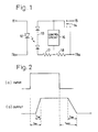
- FIGURE 1 is a circuit diagram of the semiconductor relay circuit in an embodiment according to the present invention;
- FIGS. 2(a) and 2(b) are operational waveform diagrams in the circuit of FIG. 1;
- FIG. 3 is a circuit diagram for explaining the operation of the circuit of FIG. 1;
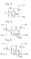
- FIG. 4 is a circuit diagram showing the semiconductor relay circuit in another embodiment according to the present invention;
- FIG. 5 a is circuit diagram showing a practical working aspect of the circuit in FIG 4;
- FIG. 6 is a circuit diagram showing the semiconductor relay circuit in a further embodiment according to the present invention;
- FIG. 7 is a circuit diagram of a practical working aspect of the circuit in FIG. 6;
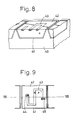
- FIG. 8 is a fragmentary perspective view of an integrated circuit employed in the semiconductor relay circuit according to the present invention, shown as sectioned along line VIII-VIII in FIG. 9; and
- FIG. 9 is a top plan view of the integrated circuit shown in FIG. 8.
- While the present invention shall now be explained with reference to the embodiments shown in the accompanying drawings, it will be appreciated that its intention is not to limit the invention only to the embodiments shown but rather to include all alterations, modifications and equivalent arrangements possible within the scope of appended claims.
- Referring to FIG. 1, the semiconductor relay circuit according to the present invention includes a pair of input terminals 11 and 11a receiving an input current signal, such light-
emitting element 12 as a light-emitting diode, preferably, which is connected between the input terminals 11 and 11a for generating a light signal in response to the input current signal, and adiode array 13 is optically coupled to the light-emittingelement 12 for generating a photovoltaic output in response to the light signal from the light-emittingelement 12. To thisdiode array 13, aMOS FET 14 is connected in series, and thisMOS FET 14 functions to vary from a first impedance state to a second impedance state upon application of the photovoltaic output across gate and source electrodes from thediode array 13, and a pair ofoutput terminal MOS FET 14. Across the gate and source electrodes of theMOS FET 14, acontrol circuit 16 is connected, a series circuit of first andsecond resistors diode array 13 and the source electrode of theMOS FET 14 while thecontrol circuit 16 is connected at its one end to a connection point between the first andsecond resistors - In the above semiconductor relay circuit, an application of the input signal across the input terminals 11 and 11a causes the light signal generated from the light-
emitting element 12, and thephotovoltaic diode array 13 which has received this light signal is to generate the photovoltaic output across the both ends of the array, upon which thecontrol circuit 16 is in a high impedance state so that a capacity across the gate and source electrodes will be charged through the first andsecond resistors diode array 13, and a voltage across the gate and source electrodes of theMOS FET 14 rises. In this case, the number of the diodes series connected in thephotovoltaic diode array 13 is set for generating a higher photovoltaic output than a threshold voltage of theMOS FET 14, so that theMOS FET 14 will be conducted across drain and source electrodes and a conduction is thereby attained across theoutput terminals MOS FET 14 rises at a rate in accordance with a capacity across the gate and source electrodes and a time constant of the first andsecond resistors output terminals MOS FET 14 to rise from zero level to a threshold value, and the rising time TUP subsequent thereto is to be a required time for the voltage across the gate and source electrodes of theMOS FET 14 to further rise from the threshold value to a saturated level. - As the input signal across the input terminals 11 and 11a is interrupted, the light signal from the light-emitting
element 12 ceases to have the generation of the photovoltaic output at thephotovoltaic diode array 13 stopped. In this event, thecontrol circuit 16 is to be varied into a low impedance state, so that an accumulated charge at the capacity across the gate and source electrodes of theMOS FET 14 will be discharged through thecontrol circuit 16 and thesecond resistor 18 in the series connected resistors, as shown by a current IOFF in FIG. 3, whereby the voltage across the gate and source electrodes of theMOS FET 14 is lowered to be below the threshold value, and theMOS FET 14 attains an interrupted state across the gate and source electrodes. Here, the voltage across the gate and source electrodes of theMOS FET 14 is decreased at a rate in accordance with the capacity across the gate and source electrodes and the time constant of thesecond resistor 18 so that, as shown in FIG. 2, the response time TOFF upon the non-conduction will be prolonged, a falling time TDN in which the output signal falls from 100% to 10% is thereby prolonged, and the falling gradient of the output signal is made gradual. Consequently, it is made possible to prevent the current from being abruptly interrupted even in an event where an inductance component is connected in series between theoutput terminals MOS FET 14 to fall from the highest level to a saturated level, and the falling time TDN subsequent thereto is to be a required time for the voltage across the gate and source electrodes of theMOS FET 14 to further fall from the saturated level to a threshold value. - As will be clear from the above, in the semiconductor relay circuit of FIG. 1, the path for flowing the current ION from the
photovoltaic diode array 13 to the gate and source electrodes of theMOS FET 14 and the further path for flowing the discharge current from the capacity across the gate and source electrodes of theMOS FET 14 to thecontrol circuit 16 respectively include each of the first andsecond resistors MOS FET 14 will be adjusted by these first andsecond resistors second resistor 18, while it will be readily appreciated that the value of theseresistors - According to another feature of the present invention, further, there is provided an arrangement which allows the both response time TON and TOFF upon the conduction and non-conduction to be settable respectively independently with an individual one of the resistors. In FIG. 4, there is shown an embodiment of this feature, in which a rectifying
element 29 is connected in parallel with thesecond resistor 28 among the series connected first andsecond resistors element 29 and through thefirst resistor 27 while the discharge current upon the non-conduction is caused to flow through thesecond resistor 28, accordingly the response time TON upon the conduction is set by thefirst resistor 27 while the response time TOFF upon the non-conduction is set by thesecond resistor 28, and thus the both response time can be set respectively independently by one of the first andsecond resistors - For the
control circuit 26 in the semiconductor relay circuit of FIG. 4, further, it is possible to employ a controlling MOS FET of a depletion type as shown in FIG. 5, in which event the controllingMOS FET 26a is connected at its drain electrode to the gate electrode of theMOS FET 24, thefirst resistor 27 is inserted between gate and source electrodes of the controllingMOS FET 26a, and the parallel circuit of thesecond resistor 28 and rectifyingelement 29 is inserted between the source electrode of theMOS FET 24 and the source electrode of the controllingMOS FET 26a. It will be appreciated that, in the arrangement, the controlling MOS FET 26a is biased to be in a high impedance state so long as the photovoltaic output is generated at thephotovoltaic diode array 23 but to be in a low impedance state when no photovoltaic output is generated. - In the arrangements shown in FIGS. 4 and 5, any other constituents than those described in the above are the same as corresponding ones in the embodiment of FIG. 1, including their function, and the same constituents as those in the embodiment of FIG. 1 are denoted by the same reference numerals but added by 10.
- According to a further feature of the present invention, there is taken a measure for improving the restricting function with respect to the electric noise without prolonging more than required the operation time upon the conduction and non-conduction, but prolonging the fall of the output signal at the response time TOFF. In FIG. 6, there is shown a circuit arrangement embodying this feature, in which a voltage
responsive element 39 is connected in parallel with thesecond resistor 38 in the series connected first andsecond resistors responsive element 39, preferably, an NMOS FET of enhancement mode having short-circuited drain and gate electrodes is employed, and this NMOS FET is to be in the low impedance state until the voltage across the gate and source electrodes of the MOS FET 34 falls to a predetermined voltage level slightly higher than the threshold voltage of the MOS FET 34, but is to be in the high impedance state once the voltage across the gate and source electrodes of the MOS FET 34 reaches below the predetermined voltage. Accordingly, the charge current upon the conduction flows through the series connected first andsecond resistors control circuit 36 as well as the voltageresponsive element 39 which is in the low impedance state at initial stage of the non-conduction, until the predetermined voltage level slightly higher that the threshold voltage of the MOS FET 34, and through thesecond resistor 36 when the voltage falls below the predetermined level and the voltageresponsive element 39 shifts to the high impedance state. The response time TOFF upon the non-conduction is thereby caused to be subjected stepwise to the current limitation of the voltageresponsive element 39 andresistor 38, the discharge rate is made gradual within the predetermined response time, and thus the falling time TDN can be prolonged to a desired extent. - For the foregoing voltage responsive element, it may be possible to employ a Zener diode, other than the NMOS FET. For the control circuit in the semiconductor relay circuit of FIG. 6, further, it will be desirable to use such controlling MOS FET 36a as shown in FIG. 7, which is substantiall of the same function as the controlling MOS FET in FIG. 5.
- In the arrangements of FIGS. 6 and 7, any other constituents than those described in the above are the same as those in the embodiment of FIG. 1, including their function, and the same constituents as those in the embodiment of FIG. 1 are denoted by the same reference numerals but added by 20.
- In manufacturing the foregoing semiconductor relay circuit in a practical working aspect of, for example, FIG. 5, in addition, a
semiconductor substrate 40 is provided in one side surface with a P-type semiconductor layer 42 formed through aninsulating film 41 comprising a silicon oxide, and an N-type semiconductor layer 43 is formed in top surface of thelayer 42. In this case, the N-type semiconductor layer 43 is formed by a diffusion in the form of a narrow zigzag strip, andaluminum wirings wiring 44 is connected to the foregoingfirst resistor 27 in the circuit of FIG. 5 while theother wiring 45 is connected to theoutput terminal 25a of the MOS FET 24 and to the P-type semiconductor layer 42. Consequent thereto, the PN junction between the P-type layer 42 and the N-type layer 43 is reversely biased when the potential at thealuminum wiring 44 is higher than that of theother wiring 45, whereas the PN junction is normally biased when the potential of thewiring 44 is lower than theother wiring 45, that is, the rectifyingelement 29 is thereby formed. Further, when the PN junction is reversely biased as in the above, a current is caused to flow from thewiring 44 through the N-type layer 43 forming a diffusion resistor to theother wiring 45, so that the second resistor is thereby formed. The value of thisresistor 28 is determined by impurity concentration, length and width of the N-type semiconductor layer 43. - With such integrated circuit as shown in FIGS. 8 and 9 utilized, the use of the rectifying
element 29 does not result in any increase in its space factor and is rather effective to render the chip area relatively small.
Claims (6)
- A semiconductor relay circuit in which a photovoltaic diode array is optically coupled to a light-emitting element to receive a light signal generated by said element upon presence of an input current thereto and to generate a photovoltaic output, an output MOS FET is connected to said photovoltaic diode array to vary from a first impedance state to a second impedance state upon application of the photovoltaic output across gate and source electrodes of said MOS FET, and a control means which is in a high impedance state upon generation of the photovoltaic output but in a low impedance state upon disappearance of the photovoltaic output is connected across the gate and source electrodes of the MOS FET, characterized in that resistors are inserted in series with respect to a path flowing a charge current from the photovoltaic diode array across the gate and source electrodes of said MOS FET and a path flowing a discharge current from a capacity across the gate and source electrodes of the MOS FET to the control means.
- A circuit according to claim 1, wherein said resistors comprise a first resistor inserted in said path flowing said charge current and a second resistor inserted in said path flowing said discharge current.
- A circuit according to claim 2, wherein a rectifying element is connected in parallel with said second resistor to be in normal direction with respect to said charge current but in reverse direction with respect to said discharge current.
- A circuit according to claim 3, wherein said rectifying element comprises a PN junction between a first semiconductor layer of one conduction type on a semiconductor substrate and a second semiconductor layer of the other conduction type formed on said first semiconductor layer, said second semiconductor layer being connected at an end to said first semiconductor layer, and said second resistor comprises said second semiconductor layer made parallel to said rectifying element upon reverse biasing of the rectifying element.
- A circuit according to claim 2, wherein a voltage responsive element is connected in parallel with said second resistor and to be in a low impedance state with respect to said discharge current and with a voltage above a predetermined level.
- A circuit according to claim 5, wherein said voltage responsive element comprises an NMOS FET of an enhancement mode and having drain and gate electrodes short-circuited.
Applications Claiming Priority (6)
| Application Number | Priority Date | Filing Date | Title |
|---|---|---|---|
| JP2034567A JPH03238918A (en) | 1990-02-15 | 1990-02-15 | Semiconductor relay circuit |
| JP34567/90 | 1990-02-15 | ||
| JP28946390A JPH0812992B2 (en) | 1990-10-26 | 1990-10-26 | Semiconductor relay circuit |
| JP289464/90 | 1990-10-26 | ||
| JP2289464A JPH0812993B2 (en) | 1990-10-26 | 1990-10-26 | Semiconductor relay circuit |
| JP289463/90 | 1990-10-26 |
Publications (2)
| Publication Number | Publication Date |
|---|---|
| EP0442561A1 true EP0442561A1 (en) | 1991-08-21 |
| EP0442561B1 EP0442561B1 (en) | 1996-05-08 |
Family
ID=27288453
Family Applications (1)
| Application Number | Title | Priority Date | Filing Date |
|---|---|---|---|
| EP91200228A Expired - Lifetime EP0442561B1 (en) | 1990-02-15 | 1991-02-05 | Semiconductor relay circuit |
Country Status (5)
| Country | Link |
|---|---|
| US (1) | US5151602A (en) |
| EP (1) | EP0442561B1 (en) |
| KR (1) | KR950000320B1 (en) |
| CA (1) | CA2035496C (en) |
| DE (1) | DE69119261T2 (en) |
Cited By (4)
| Publication number | Priority date | Publication date | Assignee | Title |
|---|---|---|---|---|
| DE4228671A1 (en) * | 1991-09-02 | 1993-03-04 | Matsushita Electric Works Ltd | SOLID RELAY |
| EP0576206A1 (en) * | 1992-06-26 | 1993-12-29 | AT&T Corp. | Break-before-make control for form C solid-state relays |
| WO1994011947A1 (en) * | 1992-11-06 | 1994-05-26 | Robert Bosch Gmbh | Circuit for protecting a mosfet power transistor |
| GB2279524A (en) * | 1993-06-22 | 1995-01-04 | Philips Electronics Uk Ltd | Gate control circuit for power MOSFET |
Families Citing this family (12)
| Publication number | Priority date | Publication date | Assignee | Title |
|---|---|---|---|---|
| US5306955A (en) * | 1991-04-22 | 1994-04-26 | Control Products, Inc. | Two-wire, electronic switch |
| JP2801825B2 (en) * | 1993-01-14 | 1998-09-21 | 株式会社東芝 | Photo coupler device |
| JPH0879041A (en) * | 1994-08-31 | 1996-03-22 | Oki Electric Ind Co Ltd | Optical semiconductor relay, controller using the same, power supply device and terminal equipment changeover device |
| US5549762A (en) * | 1995-01-13 | 1996-08-27 | International Rectifier Corporation | Photovoltaic generator with dielectric isolation and bonded, insulated wafer layers |
| US6037602A (en) * | 1998-02-13 | 2000-03-14 | C.P. Clare Corporation | Photovoltaic generator circuit and method of making same |
| US5969581A (en) * | 1998-05-28 | 1999-10-19 | The United States Of America As Represented By The Secretary Of The Navy | Opto-electronically controlled RF waveguide |
| US6555935B1 (en) * | 2000-05-18 | 2003-04-29 | Rockwell Automation Technologies, Inc. | Apparatus and method for fast FET switching in a digital output device |
| US20080238354A1 (en) * | 2007-03-29 | 2008-10-02 | Kinpo Electronics, Inc. | Solar energy charging device for computer |
| JP5027680B2 (en) * | 2008-01-18 | 2012-09-19 | パナソニック株式会社 | Semiconductor relay module |
| US7615396B1 (en) | 2008-04-28 | 2009-11-10 | Eugene Ching Lee | Photodiode stack for photo MOS relay using junction isolation technology |
| CN102332900B (en) * | 2011-10-28 | 2012-11-07 | 电子科技大学 | Solid state relay |
| US10003260B2 (en) * | 2015-06-23 | 2018-06-19 | Nxp Usa, Inc. | Semiconductor devices and methods for dead time optimization by measuring gate driver response time |
Citations (2)
| Publication number | Priority date | Publication date | Assignee | Title |
|---|---|---|---|---|
| FR2602620A1 (en) * | 1986-08-11 | 1988-02-12 | Matsushita Electric Works Ltd | SEMICONDUCTOR SWITCHING CIRCUIT |
| US4804866A (en) * | 1986-03-24 | 1989-02-14 | Matsushita Electric Works, Ltd. | Solid state relay |
Family Cites Families (6)
| Publication number | Priority date | Publication date | Assignee | Title |
|---|---|---|---|---|
| US4277098A (en) * | 1978-09-18 | 1981-07-07 | Lloyd Gibney | Foldable truck cap assembly |
| US4390790A (en) * | 1979-08-09 | 1983-06-28 | Theta-J Corporation | Solid state optically coupled electrical power switch |
| JPS6481522A (en) * | 1987-09-24 | 1989-03-27 | Agency Ind Science Techn | Optical control circuit and semiconductor device constituting said circuit |
| JPS6488528A (en) * | 1987-09-30 | 1989-04-03 | Canon Kk | Remote control signal receiver for camera |
| US5057694A (en) * | 1989-03-15 | 1991-10-15 | Matsushita Electric Works, Ltd. | Optoelectronic relay circuit having charging path formed by a switching transistor and a rectifying diode |
| JPH0758804B2 (en) * | 1989-05-17 | 1995-06-21 | 株式会社東芝 | Photo coupler device |
-
1991
- 1991-01-31 US US07/648,862 patent/US5151602A/en not_active Expired - Fee Related
- 1991-02-01 CA CA002035496A patent/CA2035496C/en not_active Expired - Fee Related
- 1991-02-05 EP EP91200228A patent/EP0442561B1/en not_active Expired - Lifetime
- 1991-02-05 DE DE69119261T patent/DE69119261T2/en not_active Expired - Fee Related
- 1991-02-12 KR KR1019910002335A patent/KR950000320B1/en not_active IP Right Cessation
Patent Citations (2)
| Publication number | Priority date | Publication date | Assignee | Title |
|---|---|---|---|---|
| US4804866A (en) * | 1986-03-24 | 1989-02-14 | Matsushita Electric Works, Ltd. | Solid state relay |
| FR2602620A1 (en) * | 1986-08-11 | 1988-02-12 | Matsushita Electric Works Ltd | SEMICONDUCTOR SWITCHING CIRCUIT |
Non-Patent Citations (1)
| Title |
|---|
| NEW ELECTRONICS.INCORPORATING ELECTRONICS TODAY. vol. 18, no. 6, March 1985, LONDON GB pages 61 - 64; P.Benfield: "Developments in solid-state-relays" * |
Cited By (5)
| Publication number | Priority date | Publication date | Assignee | Title |
|---|---|---|---|---|
| DE4228671A1 (en) * | 1991-09-02 | 1993-03-04 | Matsushita Electric Works Ltd | SOLID RELAY |
| EP0576206A1 (en) * | 1992-06-26 | 1993-12-29 | AT&T Corp. | Break-before-make control for form C solid-state relays |
| WO1994011947A1 (en) * | 1992-11-06 | 1994-05-26 | Robert Bosch Gmbh | Circuit for protecting a mosfet power transistor |
| US5424892A (en) * | 1992-11-06 | 1995-06-13 | Robert Bosch Gmbh | Circuit for protecting a MOSFET power transistor |
| GB2279524A (en) * | 1993-06-22 | 1995-01-04 | Philips Electronics Uk Ltd | Gate control circuit for power MOSFET |
Also Published As
| Publication number | Publication date |
|---|---|
| CA2035496C (en) | 1996-02-20 |
| KR910016146A (en) | 1991-09-30 |
| US5151602A (en) | 1992-09-29 |
| EP0442561B1 (en) | 1996-05-08 |
| KR950000320B1 (en) | 1995-01-13 |
| DE69119261T2 (en) | 1996-10-31 |
| CA2035496A1 (en) | 1991-08-16 |
| DE69119261D1 (en) | 1996-06-13 |
Similar Documents
| Publication | Publication Date | Title |
|---|---|---|
| EP0442561B1 (en) | Semiconductor relay circuit | |
| US7209332B2 (en) | Transient detection circuit | |
| JP2759577B2 (en) | Buffer circuit | |
| US4581540A (en) | Current overload protected solid state relay | |
| US5428310A (en) | Voltage compensating delay element | |
| US4801822A (en) | Semiconductor switching circuit | |
| EP0029681B1 (en) | Bias-voltage generator | |
| KR900004196B1 (en) | Voltage level sensing power-up reset circuit | |
| EP0463854B1 (en) | Clocked driver circuit | |
| US6369556B2 (en) | Power supply control device and method | |
| US6353353B1 (en) | Integrated semiconductor circuit with improved power supply control | |
| EP0425035A2 (en) | Overload protection drive circuit for a power transistor | |
| US5276370A (en) | MOS-type semiconductor device drive circuit | |
| US5847593A (en) | Voltage discharge circuit for a photovoltaic power source | |
| US4321561A (en) | Switch operated capacitive oscillator apparatus | |
| EP0645890B1 (en) | BiCMOS logic circuit | |
| US5396120A (en) | Semiconductor integrated unit | |
| JP2541325B2 (en) | Output buffer circuit | |
| JPH0151091B2 (en) | ||
| JPH06216736A (en) | Solid-state relay with varistor | |
| JPH05243949A (en) | Solid state relay | |
| JPH0537322A (en) | Output circuit for control signal | |
| JPH0151092B2 (en) | ||
| JPH09172177A (en) | Semiconductor device with zener diode | |
| JPH0812992B2 (en) | Semiconductor relay circuit |
Legal Events
| Date | Code | Title | Description |
|---|---|---|---|
| PUAI | Public reference made under article 153(3) epc to a published international application that has entered the european phase |
Free format text: ORIGINAL CODE: 0009012 |
|
| AK | Designated contracting states |
Kind code of ref document: A1 Designated state(s): DE FR GB |
|
| 17P | Request for examination filed |
Effective date: 19910726 |
|
| 17Q | First examination report despatched |
Effective date: 19940412 |
|
| GRAA | (expected) grant |
Free format text: ORIGINAL CODE: 0009210 |
|
| AK | Designated contracting states |
Kind code of ref document: B1 Designated state(s): DE FR GB |
|
| REF | Corresponds to: |
Ref document number: 69119261 Country of ref document: DE Date of ref document: 19960613 |
|
| ET | Fr: translation filed | ||
| PLBE | No opposition filed within time limit |
Free format text: ORIGINAL CODE: 0009261 |
|
| STAA | Information on the status of an ep patent application or granted ep patent |
Free format text: STATUS: NO OPPOSITION FILED WITHIN TIME LIMIT |
|
| 26N | No opposition filed | ||
| K1C1 | Correction of patent application (title page) published |
Effective date: 19910821 |
|
| REG | Reference to a national code |
Ref country code: GB Ref legal event code: 746 Effective date: 19990428 |
|
| REG | Reference to a national code |
Ref country code: FR Ref legal event code: D6 |
|
| PGFP | Annual fee paid to national office [announced via postgrant information from national office to epo] |
Ref country code: DE Payment date: 20010129 Year of fee payment: 11 |
|
| PGFP | Annual fee paid to national office [announced via postgrant information from national office to epo] |
Ref country code: GB Payment date: 20010131 Year of fee payment: 11 |
|
| PGFP | Annual fee paid to national office [announced via postgrant information from national office to epo] |
Ref country code: FR Payment date: 20010213 Year of fee payment: 11 |
|
| REG | Reference to a national code |
Ref country code: GB Ref legal event code: IF02 |
|
| PG25 | Lapsed in a contracting state [announced via postgrant information from national office to epo] |
Ref country code: GB Free format text: LAPSE BECAUSE OF NON-PAYMENT OF DUE FEES Effective date: 20020205 |
|
| PG25 | Lapsed in a contracting state [announced via postgrant information from national office to epo] |
Ref country code: DE Free format text: LAPSE BECAUSE OF NON-PAYMENT OF DUE FEES Effective date: 20020903 |
|
| GBPC | Gb: european patent ceased through non-payment of renewal fee |
Effective date: 20020205 |
|
| PG25 | Lapsed in a contracting state [announced via postgrant information from national office to epo] |
Ref country code: FR Free format text: LAPSE BECAUSE OF NON-PAYMENT OF DUE FEES Effective date: 20021031 |
|
| REG | Reference to a national code |
Ref country code: FR Ref legal event code: ST |