EP0441388B1 - Semiconductor memory circuit - Google Patents
Semiconductor memory circuit Download PDFInfo
- Publication number
- EP0441388B1 EP0441388B1 EP91101718A EP91101718A EP0441388B1 EP 0441388 B1 EP0441388 B1 EP 0441388B1 EP 91101718 A EP91101718 A EP 91101718A EP 91101718 A EP91101718 A EP 91101718A EP 0441388 B1 EP0441388 B1 EP 0441388B1
- Authority
- EP
- European Patent Office
- Prior art keywords
- circuit
- load
- transistors
- sense amplifier
- current
- Prior art date
- Legal status (The legal status is an assumption and is not a legal conclusion. Google has not performed a legal analysis and makes no representation as to the accuracy of the status listed.)
- Expired - Lifetime
Links
Images


Classifications
-
- G—PHYSICS
- G11—INFORMATION STORAGE
- G11C—STATIC STORES
- G11C7/00—Arrangements for writing information into, or reading information out from, a digital store
- G11C7/12—Bit line control circuits, e.g. drivers, boosters, pull-up circuits, pull-down circuits, precharging circuits, equalising circuits, for bit lines
-
- G—PHYSICS
- G11—INFORMATION STORAGE
- G11C—STATIC STORES
- G11C11/00—Digital stores characterised by the use of particular electric or magnetic storage elements; Storage elements therefor
- G11C11/21—Digital stores characterised by the use of particular electric or magnetic storage elements; Storage elements therefor using electric elements
- G11C11/34—Digital stores characterised by the use of particular electric or magnetic storage elements; Storage elements therefor using electric elements using semiconductor devices
- G11C11/40—Digital stores characterised by the use of particular electric or magnetic storage elements; Storage elements therefor using electric elements using semiconductor devices using transistors
- G11C11/41—Digital stores characterised by the use of particular electric or magnetic storage elements; Storage elements therefor using electric elements using semiconductor devices using transistors forming static cells with positive feedback, i.e. cells not needing refreshing or charge regeneration, e.g. bistable multivibrator or Schmitt trigger
- G11C11/413—Auxiliary circuits, e.g. for addressing, decoding, driving, writing, sensing, timing or power reduction
- G11C11/414—Auxiliary circuits, e.g. for addressing, decoding, driving, writing, sensing, timing or power reduction for memory cells of the bipolar type
- G11C11/416—Read-write [R-W] circuits
Definitions
- the present invention relates to a semiconductor memory circuit, and more particularly to a semiconductor memory circuit that uses micro-miniaturized elements, for which are required a high degree of integration and a high speed of operation.
- each memory cell is connected to corresponding one of digit line pairs and corresponding one of word lines, and each load device and sense amplifier are connected via the digit line pair.
- Fig.1 is a semiconductor memory circuit diagram in a prior art.
- the conventional semiconductor memory circuit includes a memory cell 1 connected to a word line WL and to a digit line pair D1 and D1 ⁇ , a load circuit 11 and a switching circuit 12 that are connected through the digit line pair D1 and D1 ⁇ to a sense amplifier circuit 13.
- Memory cells 1A and 1B are similar to the memory cell 1; load circuits 11A and 11B are also similar to the load circuit 11; switching circuits 12A and 12B are also similar to the switching circuit 12 and digit line pairs D2 and D2 ⁇ , D3 and D3 ⁇ are also similar to the digit line pair D1 and D1 ⁇ , so that only one set will be taken up and other sets will be omitted unless otherwise needed in the description that will follow.
- the memory cell 1 includes a flip-flop composed of resistor elements R1 and R2 and N channel type insulated gate field effect transistors (hereinafter referred to "NMOS transistors” in plural case and “NMOS transistor” in singular case) MC3 and MC4 (cell transistors), and a switching means for transmission composed of NMOS transistors MC1 and MC2 connected between the digit line pair D1 and D1 ⁇ , and the word line WL.
- NMOS transistors N channel type insulated gate field effect transistors
- MC3 and MC4 cell transistors
- cell information can be detected as a potential difference between the digit line pair D1 and D1 ⁇ by means of the conductance ratio of the cell transistors MC3 and MC4, and P channel type insulated gate field effect transistors (hereinafter referred to "PMOS transistors” in plural case and “PMOS transistor” in singular case) M18 and M19 as load elements in the load circuit 11 that are connected to the digit lines D1 and D1 ⁇ .
- PMOS transistors P channel type insulated gate field effect transistors
- the switching circuit 12 includes PMOS transistors M20 and M21 as the switching elements that are connected to the digit line pair D1 and D1 ⁇ and are supplied with a digit selection signal Y1 to their gates, a PMOS transistor M22 that connects between the digit lines, and an inverter INV which supplies the digit selection signal Y1 to the gate of the PMOS transistor M22 by inverting it.
- the switching circuit 12 sends out the information in the memory cell 1 to the data buses DB and DB ⁇ via the switching PMOS transistors M20 and M21 that are turned on by the digit selection signal Y1.
- Information from a plurality of switching circuits 12, 12A and 12B is transmitted to the data buses DB and DB ⁇ by means of a multiplexer operation, and then transferred to the sense amplifier circuit 13.
- the sense amplifier circuit 13 includes the input bipolar transistors Q18 and Q19, the differential amplifier bipolar transistors Q20 and Q21, the load resistor elements R9 and R10 and NMOS transistors M23 to M25 that form a constant current source for input emitter-followers and ECL current stitches.
- the sense amplifier circuit 13 supplies a potential difference information detected between the digit lines D1 and D1 ⁇ as a difference potential (SB, SB ⁇ ) to the bases of the emitter-coupled bipolar transistors Q20 and Q21 that form a differential amplifier via the input bipolar transistors Q18 and Q19 of the emitter-followers, and output it from S and S ⁇ by amplifying it to a difference potential sufficient to operate an output buffer (not shown) by means of the load impedance elements R9 and R10 connected to the collectors of the bipolar transistors Q20 and Q21.
- SB, SB ⁇ difference potential
- the levels in which the digit lines D1 and D1 ⁇ are in a non-selected state go to potentials which are substantially equal with each other by means of the PMOS transistor M22 for digit line equalization whose gate receives the signal obtained by inverting a digit selection signal Y1 of the switching circuit 12 using the inverter INV, and the digit lines D1 and D1 ⁇ are in a standby state in order to read the information of the memory cell 1 at high speed in a selected state.
- information within the memory cell is detected as the difference between the left and right digit line potentials determined by the conductance ratio of the load PMOS transistors M18, M19 connected respectively to the digit lines D1, D1 ⁇ that form a pair of left and right lines and the NMOS transistors MC1 to MC4 of the selected memory cell, and the information thus detected is input to the sense amplifier 13 via the switching PMOS transistors M20, M21.
- the conventional semiconductor memory circuit described above reads the cell information as the difference between the digit line potentials that are determined by the conductance ratio of the load MOS transistors connected to the memory cell via a digit line pair and the MOS transistors within the memory cell, and leads the information to a sense amplifier.
- the difference between the source-drain voltages of the load MOS transistors generated by the difference between the currents that flow into the cell (cell current) from either of the left or right digit line of the memory cell is set to be the digit line potential difference.
- a high-speed reading operation requires a high-speed driving of the digit lines.
- the capacitance of the diffused region of the source of a memory cell MOS transistors that is used in large number for parallel connection has a magnitude of about several tens of picofarads. Consequently, MOS transistors with high driving capability are required in order to perform high-speed charging or discharging. It should be noted further that what lifts the digit line potential to a high level is a load MOS transistor while what lowers it is a MOS transistor in the cell.
- US-A-4 829 479 discloses a semiconductor memory circuit according to the precharacterizing portion of claim 1. In this circuit a common power voltage is connected through a MOS-field-effect transistor for pull up the memory cell.
- an object of the present invention in to provide a semiconductor memory circuit in which an adverse effect due to unbalances among transistors such as NMOS transistors constituting the memory cell is eliminated thereby realizing a high speed operation and a high production yield.
- the present semiconductor memory circuit is constructed in such a way that the information of the memory cell is read by the use of the potential difference of the forward voltages generated by supplying the cell current that is made to flow in either of the digit line pair as the difference between the forward currents of the diode type semiconductor elements using p-n junctions connected respectively to the digit line pair and the data bus line pair, and transmits the information to the sense amplifier.
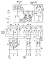
- Fig. 2 is a circuit diagram of a semiconductor memory circuit showing a first embodiment of the present invention.
- the present embodiment includes memory cells 1, 1A to 1E that are arranged at the intersections of word lines WL1 and WL2, and digit line pairs D1 and D1 ⁇ to D3 and D3 ⁇ , switching circuits 2, 2A and 2B that are connected between these digit line pairs and a bus line pair (DB, DB ⁇ ) 7, and a read circuit 3 which includes a load circuit 4 connected to the bus line pair 7, a constant current source circuit 5 and a sense amplifier circuit 6.
- the memory cells 1, 1A to 1E are constructed by a flip-flop type memory information holding part which has NMOS transistors MC3 and MC4 and resistor elements RC1 and RC2, and NMOS transistors MC1 and MC2 for information transmission connected between the flip-flop type memory information holding part and digit lines D1 and D1 ⁇ .
- the gates of the NMOS transistors MC1 and MC2 are connected to the word line WL1, and a memory cell array is formed by arranging a plurality of these memory cells, word lines and digit line pairs in matrix form.
- the digit lines D1 and D1 ⁇ are connected to the digit line switching circuit 2 which is switched by a Y1 signal, and, at the time of selection, they are connected respectively to data bus line pair DB and DB ⁇ which collect the information of the digit lines via an inverter INV and PMOS transistors M1 and M2. Further, at the time of nonselection of the switching circuit 2, the digit lines D1 and D1 ⁇ are connected via PMOS transistors M3 and M4 to a DBL (Data Bus Low Level) line which is set at a potential for digit line non-selection, that is, at a standby potential.
- DBL Data Bus Low Level
- the data buses DB and DB ⁇ connected to the digit lines that are selected by a multiplexer operation by means of a plurality of the dight line switching circuits 2, 2A and 2B are connected to the cathodes of diode type semiconductor elements (load diodes), such as the Q1 and Q2 that are p type - n type semiconductor junction diodes.
- load diodes diode type semiconductor elements
- the data bus line pair DB and DB ⁇ are fixed to Vcc minus about 0.8 V, and the digit lines D1 and D1 ⁇ are brought to the potentials that are determined by the conductance ratio of the switching PMOS transistors M1 and M2, and the NMOS transistors for transmission MC1 and M2 and the NMOS transistors for data holding MC3 and MC4.
- the load diodes Q1 and Q2 are connected to a constant current source circuit 5 including NMOS transistors MC5 to MC8 that simulate the memory cell structure and resistance elements RC3 and RC4, for keeping a minute offset current I1', I2', for example, of 0.001 mA (1 ⁇ A), respectively, to be passed even when there are flowing no cell currents, so that unstable floating state is avoided. Namely, when a cell current I1 is flowing in the load diode Q1 (in total I1 + I2'), there is flowing its offset current I1' alone in the load diode Q2.
- the value of the offset current I1' is determined by the NMOS transistors MC5 and MC7 which have the direction and the shape same as those of the NMOS transistors except the width, for example that are on the energized side of the selected memory cell 1.
- the gate channel width W of the MC1 and the MC5 is set to an appropriate preset constant value; for example, the ratio of the width of the MC1 to that of MC5 is 100 to 1; absolute value of the impedances of these NMOS transistors MC1, MC5 are sufficiently large compared with the impedances of the MOS transistors for cell holding or the impedances of the switching MOS transistors, so that the current ratio of I1 and I1' becomes equal to the preset constant value.
- the sense amplifier circuit 6 shown in this embodiment amplifies the potential difference which enters the gates of the NMOS transistors M5 and M6 by the use of a current mirror circuit formed by the PMOS transistors M7 and M8, and outputs the result from an output terminal S.
- the amplified output becomes a data output through an output buffer. It should be mentioned that the case in which the output S of the sense amplifier circuit 6 has one terminal is shown in this example, but it may have two terminals (S and S ⁇ ).
- the potential DBL for non-selection is set to Vcc minus about 0.8 V which is the same level as at the time of selection by means of a diode Q3 that simulate the load diodes Q1 and Q2, and all of the digit lines in the non-selected state are clamped at this voltage.
- Fig. 3 is a timing chart of the internal potential for describing the read operation of the semiconductor memory circuit.
- the word line WL is switched with a delay through a decoder.
- the selected cell is shifted, and the height relationship of the potentials that appear on the digit lines and the data bus lines is inverted.
- the waveforms of DB and DB ⁇ shown in the figure represent the above-mentioned situation, and the amplitudes of the potentials are suppressed to small values of about 100 mV in order to have a switching at high speed, in view of the slow speed of the potential change due to a large capacitance added to the digit lines.
- the potential difference between the data buses DB and DB ⁇ varies as much as about 40 mV at the worst for 100 mV by the nonuniformity in the device characteristics generated between paired devices such as the MOS transistors in the memory cell, the load MOS transistors and the switching MOS transistors.
- the amplitude of the data buses DB and DB ⁇ it becomes necessary to increase the amplitude of the data buses DB and DB ⁇ to about 150 mV in order to secure the margin with the capability limit of the sense amplifier 6, which also generates a delay of several nanoseconds in the address access time T.
- Fig. 4 is a diagram for the forward current-voltage characteristic of a p-n junction diode constituting a load circuit shown in Fig. 2.
- ⁇ V kT q ⁇ log I - log I' + log (1 + I s I )- log (1 + I s I' ) ⁇ ⁇ kT q ⁇ log I - log I' ⁇ (I » I s an I' » I s ) ⁇ K log ( I I' ) (K; const.)
- the potential difference between the data buses DB and DB ⁇ is determined by I/I' provided that the cell current I is sufficiently large compared with the offset current I'.
- the devices for raising the potentials of the digit lines D1 and D1 ⁇ and the potentials of the data bus lines DB and DB ⁇ are the load diodes Q1 and Q2.
- a p-n junction element has a higher current supply capability than a MOS transistor, and in one semiconductor chip, deviation of characteristics among p-n junction elements are far small than that among MOS transistors. Therefore, these are optimum as the high-speed driving elements of the high capacity portions which will enable to obtain a substantial increases in the operating speed and a stability of the characteristics.
- diodes type semiconductor elements such as the p-n junction type diodes are used as load devices by connecting then in the forward direction.
- a digit line switching MOS transistor is installed between the diode type semiconductor element, namely, the load diode, and the digit line, which is connected to the load diode via a data bus which collected the digit information.
- the potential difference between the forward voltages generated in the load diodes that form a left and right pair may be directly input to the sense amplifier without the intermediary of an MOS transistor switching circuit.
- offset currents that flow in these load diodes may be supplied in the present embodiment by installing constant current sources that simulate the cell.
- the potential difference DB/ DB ⁇ inputting the sense amplifier circuit 6 is not affected by the unbalance because the difference DB/ DB ⁇ is determined by the ratio of currents flowing the load diodes Q1 and Q2.
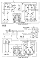
- Fig. 5 is a read circuit diagram in the semiconductor memory circuit for describing a second embodiment of the present invention.
- the present embodiment has, in comparison with the first embodiment in Fig. 2, the sense amplifier 6A constructed by bipolar transistors Q6 to Q9, and bipolar transistors Q4, Q5 for switching installed between the load circuit 4 and the constant current source 5.
- signals are supplied to a bipolar differential amplifier type sense amplifier circuit 6A from the cathodes of the load devices Q1 and Q2 through bipolar transistors Q4 and Q5 that are emitter-follower connected and through the wirings of SB and SB ⁇ .
- the operation of the sense amplifier circuit 6A is the same as that of the sense amplifier 13 of the prior art shown in Fig. 1 described above. Since a circuit which is precisely the same as that of the memory cell 1 (Fig.
- the level of the currents from the constant current sources 5 are the same as the level of the cell currents.
- the offset currents of the load diodes Q1 and Q2 become the base currents of the transistors Q4 and Q5, being I1/h fe and I2/h fe for the cells on the left and the right, respectively. Therefore, the potential difference of the load diodes Q1 and Q2 is given by ⁇ V ⁇ K log (h fe ) from Eq. (2) explained before, and is controlled exclusively by the amplification factor h fe of the bipolar transistors Q4 and Q5.
- h fe is about 100 so that the potential difference ⁇ V of the load diodes Q1 and Q2 becomes about 120 mV and a required potential difference can sufficiently be obtained.
- the currents of the current sources CS4 and CS5 for the input emitter-followers of the sense amplifier circuit 6A are about several hundred microamperes, and therefore, the base currents of the bipolar transistors Q6 and Q7 become several microamperes which values are sufficiently small comparing with the emitter currents of the bipolar transistors Q4 and Q5, and hence can be neglected. Since, the above-mentioned sense amplifier circuit 6A is an ECL circuit, it is possible to realize a sufficiently high speed switching with a potential difference of about 100 mV.
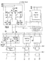
- Fig. 6 is a read circuit diagram of a third embodiment of the present invention, and is similar to Fig. 5.
- the present embodiment is an example of a large capacity memory circuit which is formed by assembling a plurality of read circuit blocks 3, with one read circuit block 3 being formed by the circuit up to the sense amplifier circuit 6B.
- the load diodes Q1 and Q2 that constitute a load circuit 4, a constant current source circuit 5 for offset current and a sense amplifier circuit 6B are substantially the same as the first or the second embodiment described in the above. The difference is that the outputs from the sense amplifier circuit 6B are taken out from the collectors of bipolar transistors Q12 and Q13 to read buses RB and RB ⁇ , to which many read circuit blocks 3 are connected at their collectors of bipolar transistors Q12 and Q13.
- difference currents are input to emitters of bipolar transistors Q14 and Q15 constituting a differential amplifier of a sense amplifier circuit 6C.
- the bases of the bipolar transistors Q14 and Q15 are commonly connected to each other and keep a base potential SB.
- amplitude output signals S and S ⁇ obtained by the bipolar transistors Q14 and Q15, resistor elements R7 and R8 and constant current source circuits CS6 and CS7 are output.
- a common block selection signal YS is supplied to the gates of all of the NMOS transistors M9 to M11 for constant current sources of the sense amplifier circuit 6B and the NMOS transistors MC5 and MC6 of the constant current source circuit 5 for offset current, so that the current in the block that flows at the time of block nonselection becomes substantially zero and it is possible to realize a lower-power and a high-speed memory circuit.
- Fig. 7 is a semiconductor memory circuit diagram showing a fourth embodiment of the present invention.
- the present embodiment is an example of a circuit in which a constant current source for offset current of a load diode that constitutes a load circuit 4 is provided for each of the digit line pairs D1 and D1 ⁇ to D3 and D3 ⁇ in order to generate more accurate data for the ratios of the cell currents I1 and I2 (Fig. 2) and the offset currents I1' and I2' (Fig. 2).
- the constant source circuits 8, 8A and 8B are selected by the use of selection signals Y1 to Y3 of the switching circuits 2, 2A and 2B for digit line selection. Accordingly, a selection memory cell 1 and the constant current source circuit 8 which simulates the memory cell 1 as in Fig.
- Fig. 8 is a semiconductor memory circuit diagram showing a fifth embodiment of the present invention.
- the embodiment is an example of applying the present invention to a circuit for write operation.
- the load diode part forms a write circuit 9
- the constitution of a digit line switching circuit 10 differs from those of the first to the fourth embodiments.
- NMOS transistors M14 and M15 in parallel with PMOS transistors M12 and M13 in the switching circuit 10.
- the output W2 of a NOR gate that has the control signals WD and WD ⁇ as the inputs energizes an NMOS transistor MW7 for equalizing the potentials between the bases of the p-n junction load diodes Q16 and Q17, removes a minute base potential difference due to an unbalance between the PMOS transistors MW1, MW2, and eliminate a nonuniformity due to MOS transistors.
- either of the control signals WD and WD ⁇ is raised to a high level (potential Vcc) by the write data.
- a high level potential Vcc
- an output W1 of the CMOS inverter including the PMOS transistor MW1 and the NMOS transistor MW3 in the write circuit 9 goes to the low level, and an NMOS transistor MW5 is turned on at the same time when the bipolar transistor Q16 is turned off, so that the charges on the data bus line DB and the digit line D1 are discharged and their potentials are lowered to the low (V EE ) potential.
- the NMOS transistor MW7 for equalization is de-energized at this time.
- the PMOS transistor MW1 and the NMOS transistor MW7 in the write circuit 9 are energized and W1 which is the base potential of the bipolar transistor Q16 is raised, so that the potentials of the data bus DB and the digit line D1 are quickly elevated by the action of the high capability bipolar transistors making it possible to enter the read state.
- the semiconductor memory circuit in accordance with the present invention a load circuit for the memory cell transistors is formed by the use of diode type semiconductor elements, and the memory cell information is read by means of a forward potential difference that is generated according to the ratio of the currents that flow in the diode type semiconductor element pairs of the load circuit. Therefore, it becomes possible to eliminate the read potential fluctuations due to unbalances in the characteristics of the paired transistors in the memory cells and on the digit line pairs. Further, the present invention has an effect that enables the realization of a read operation at high speed and with small nonuniformity of the velocity.
- the semiconductor memory circuit of the present invention it becomes possible to drive the data bus lines and the digit lines with large capacity load, by forming a diode type semiconductor element pair that forms a load circuit with bipolar transistors, and by using these read circuit systems as a part of the write circuit. Therefore, the present invention has an effect of realizing a high-speed write operation and a recovery operation from the writing mode using a small number of elements.
Landscapes
- Engineering & Computer Science (AREA)
- Microelectronics & Electronic Packaging (AREA)
- Computer Hardware Design (AREA)
- Static Random-Access Memory (AREA)
- Dram (AREA)
Description
- The present invention relates to a semiconductor memory circuit, and more particularly to a semiconductor memory circuit that uses micro-miniaturized elements, for which are required a high degree of integration and a high speed of operation.
- In a semiconductor memory circuit, each memory cell is connected to corresponding one of digit line pairs and corresponding one of word lines, and each load device and sense amplifier are connected via the digit line pair.
- Fig.1 is a semiconductor memory circuit diagram in a prior art. The conventional semiconductor memory circuit includes a
memory cell 1 connected to a word line WL and to a digit line pair D1 and
load circuit 11 and aswitching circuit 12 that are connected through the digit line pair D1 and
sense amplifier circuit 13.Memory cells memory cell 1;load circuits load circuit 11; switchingcircuits switching circuit 12 and digit line pairs D2 and


- First, the
memory cell 1 includes a flip-flop composed of resistor elements R₁ and R₂ and N channel type insulated gate field effect transistors (hereinafter referred to "NMOS transistors" in plural case and "NMOS transistor" in singular case) MC3 and MC4 (cell transistors), and a switching means for transmission composed of NMOS transistors MC1 and MC2 connected between the digit line pair D1 and
memory cell 1 and the digit line pair D1 and

load circuit 11 that are connected to the digit lines D1 and
- The
switching circuit 12 includes PMOS transistors M20 and M21 as the switching elements that are connected to the digit line pair D1 and
switching circuit 12 sends out the information in thememory cell 1 to the data buses DB and
switching circuits 
sense amplifier circuit 13. - Moreover, the
sense amplifier circuit 13 includes the input bipolar transistors Q18 and Q19, the differential amplifier bipolar transistors Q20 and Q21, the load resistor elements R9 and R10 and NMOS transistors M23 to M25 that form a constant current source for input emitter-followers and ECL current stitches. In particular, thesense amplifier circuit 13 supplies a potential difference information detected between the digit lines D1 and


- Here, the levels in which the digit lines D1 and

switching circuit 12 using the inverter INV, and the digit lines D1 and
memory cell 1 at high speed in a selected state. - In addition, at the time of writing, by lowering the potential of either of the digit line pair D1 and

memory cell 1, one of the NMOS transistors MC3 and MC4 that is energized of the flip-flop can be turned off and the internal state of thememory cell 1 can be inverted, so that it becomes possible to carry out writing to thememory cell 1. - In short, in the prior art semiconductor memory circuit described in the above, information within the memory cell is detected as the difference between the left and right digit line potentials determined by the conductance ratio of the load PMOS transistors M18, M19 connected respectively to the digit lines D1,

sense amplifier 13 via the switching PMOS transistors M20, M21. - The conventional semiconductor memory circuit described above reads the cell information as the difference between the digit line potentials that are determined by the conductance ratio of the load MOS transistors connected to the memory cell via a digit line pair and the MOS transistors within the memory cell, and leads the information to a sense amplifier. The difference between the source-drain voltages of the load MOS transistors generated by the difference between the currents that flow into the cell (cell current) from either of the left or right digit line of the memory cell, is set to be the digit line potential difference.
- Now, a high-speed reading operation requires a high-speed driving of the digit lines. However, the capacitance of the diffused region of the source of a memory cell MOS transistors that is used in large number for parallel connection has a magnitude of about several tens of picofarads. Consequently, MOS transistors with high driving capability are required in order to perform high-speed charging or discharging. It should be noted further that what lifts the digit line potential to a high level is a load MOS transistor while what lowers it is a MOS transistor in the cell.
- Therefore, there are disadvantages that when the transistor driving capability is raised, the potential difference between the digit lines becomes small in the former while the cell current is increased in the latter.
- Because of this fact, in order to realize a circuit for high-speed reading one has to design the circuit constants so as to have a minimum digit line amplitude that permits the operation of a sense amplifier for an allowable maximum cell current.
- In addition, in a semiconductor memory circuit which employs microdevices for which is required a high speed operation, when there is generated a manufacturing error to cause an unbalance in the characteristics of the left and the right MOS transistors within a cell (unbalance between MC1 and MC2, and/or unbalance between MC3 and MC4), load MOS transistors (unbalance between M18 and M19) and switching MOS transistors (unbalance between M20 and M21), there are generated deviations in the high levels and the low levels of the currents that flow in the left and the right data buses connected to the
sense amplifier 13. Consequently, the minimum potential difference for detecting the information is reduced. - The nonuniformity in the device properties which has its origin in the fabrication of the devices is observed more frequently in MOS transistors. For example, in a device with gate length of L = 1.0 µm, it is inevitable in the manufacturing process to generate an error of about ±0.1 µm. By interacting the error with other nonuniformity in characteristics, the sense amplifier input potential difference reduces to about 100 mV to 60 mV, so that it becomes necessary to design a circuit with a preset margin. When a margin is taken for each element, there arises another disadvantage that the operating speed is reduced for a circuit memory as a whole.
- Moreover, even in a circuit for which an operating margin is secured, when there are generated unbalances in the device characteristics, the reading speed to have a nonuniformity depending upon the memory cell selected, which leads to a reduction in the access speed for a memory circuit as a whole. Further, this also becomes a cause for an increase in the nonuniformity of the characteristics of the products, and gives rise also to a drawback which causes a reduction in the yield. US-A-4 829 479 discloses a semiconductor memory circuit according to the precharacterizing portion of
claim 1. In this circuit a common power voltage is connected through a MOS-field-effect transistor for pull up the memory cell. - Therefore, an object of the present invention in to provide a semiconductor memory circuit in which an adverse effect due to unbalances among transistors such as NMOS transistors constituting the memory cell is eliminated thereby realizing a high speed operation and a high production yield.
- According to the present invention this object is achieved by a semiconductor memory circuit according to
claim 1. - The present semiconductor memory circuit is constructed in such a way that the information of the memory cell is read by the use of the potential difference of the forward voltages generated by supplying the cell current that is made to flow in either of the digit line pair as the difference between the forward currents of the diode type semiconductor elements using p-n junctions connected respectively to the digit line pair and the data bus line pair, and transmits the information to the sense amplifier.
-
- Fig. 1 is a circuit diagram showing a conventional semiconductor memory circuit;
- Fig. 2 is a circuit diagram showing a first embodiment of the present invention;
- Fig. 3 is a timing chart showing internal potentials during a reading operation in the semiconductor memory circuit;
- Fig. 4 is a diagram showing forward current vs voltage characteristics of the diode in the load circuit of Fig. 2;
- Fig. 5 is a circuit diagram showing a read circuit in a second embodiment of the present invention;
- Fig. 6 is a circuit diagram showing read circuits, a sense amplifier circuit and a connecting means therebetween in a third embodiment of the present invention;
- Fig. 7 is a circuit diagram showing a fourth embodiment of the present invention; and
- Fig. 8 is a circuit diagram showing a fifth embodiment of the present invention.
- Next, referring to the drawings, the embodiments of the present invention will be explained.
- Fig. 2 is a circuit diagram of a semiconductor memory circuit showing a first embodiment of the present invention.
- As shown in Fig. 2, the present embodiment includes
memory cells 

circuits 
read circuit 3 which includes a load circuit 4 connected to the bus line pair 7, a constantcurrent source circuit 5 and asense amplifier circuit 6. - Now, a reading operation will be described.
- First, the
memory cells memory cell 1 as the representative hereinafter) are constructed by a flip-flop type memory information holding part which has NMOS transistors MC3 and MC4 and resistor elements RC1 and RC2, and NMOS transistors MC1 and MC2 for information transmission connected between the flip-flop type memory information holding part and digit lines D1 and

line switching circuit 2 which is switched by a Y1 signal, and, at the time of selection, they are connected respectively to data bus line pair DB and
switching circuit 2, the digit lines D1 and

line switching circuits 

memory cell 1 is energized, such reading of the information of thememory cell 1 is detected as the difference between the forward voltages of the load diode pair Q1 and Q2 generated by the presence or absence of the cell currents I₁, I₂, for example, of 0.1 mA, respectively, that flows from the digit on the energized side to a lowest voltage VEE through thememory cell 1, namely, as the potential difference between the data buses DB and
current source circuit 5 including NMOS transistors MC5 to MC8 that simulate the memory cell structure and resistance elements RC3 and RC4, for keeping a minute offset current I₁', I₂', for example, of 0.001 mA (1 µA), respectively, to be passed even when there are flowing no cell currents, so that unstable floating state is avoided. Namely, when a cell current I₁ is flowing in the load diode Q1 (in total I₁ + I₂'), there is flowing its offset current I₁' alone in the load diode Q2. The value of the offset current I₁' is determined by the NMOS transistors MC5 and MC7 which have the direction and the shape same as those of the NMOS transistors except the width, for example that are on the energized side of theselected memory cell 1. When a part of the device parameters, for example, the gate channel width W of the MC1 and the MC5, is set to an appropriate preset constant value; for example, the ratio of the width of the MC1 to that of MC5 is 100 to 1; absolute value of the impedances of these NMOS transistors MC1, MC5 are sufficiently large compared with the impedances of the MOS transistors for cell holding or the impedances of the switching MOS transistors, so that the current ratio of I₁ and I₁' becomes equal to the preset constant value. For example, when the constant is set to 100, the offset current I₂' that flows in the diode Q1 is sufficiently small compared with I₁ and can be ignored, so that the current ratio of the load diodes becomes equal to 100. Accordingly, the potential of the data bus DB becomes about 120 mV lower than that of the data bus
sense amplifier circuit 6. Thesense amplifier circuit 6 shown in this embodiment amplifies the potential difference which enters the gates of the NMOS transistors M5 and M6 by the use of a current mirror circuit formed by the PMOS transistors M7 and M8, and outputs the result from an output terminal S. The amplified output becomes a data output through an output buffer. It should be mentioned that the case in which the output S of thesense amplifier circuit 6 has one terminal is shown in this example, but it may have two terminals (S and
- Here, the potential DBL for non-selection is set to Vcc minus about 0.8 V which is the same level as at the time of selection by means of a diode Q3 that simulate the load diodes Q1 and Q2, and all of the digit lines in the non-selected state are clamped at this voltage.
- Next, the internal switching will be described by making reference to the change in time of the potential waveform.
- Fig. 3 is a timing chart of the internal potential for describing the read operation of the semiconductor memory circuit.
- As shown in Fig. 3, the operation of word address access will be dealt with in the following.
- First, when the address input is switched at the respective times of t1 and t2, the word line WL is switched with a delay through a decoder. As a result of this operation, the selected cell is shifted, and the height relationship of the potentials that appear on the digit lines and the data bus lines is inverted. The waveforms of DB and

sense amplifier 6, and are taken out as outputs S and


sense amplifier 6, and eventually a malfunction is brought about. - In the prior art circuit shown in Fig. 1 described above, the potential difference between the data buses DB and


sense amplifier 6, which also generates a delay of several nanoseconds in the address access time T. - Next, referring to Fig. 4, such a potential setting for the data buses DB and

- Fig. 4 is a diagram for the forward current-voltage characteristic of a p-n junction diode constituting a load circuit shown in Fig. 2.
- As shown in Fig. 4, in the current region where the series resistance component of the diode can be neglected, the current obeys the following Eq. (1).

- Further, the potential difference ΔV generated by the cell current I and the offset current I' is given by the following Eq. (2).

- Is:
- BJT saturation current
- q :
- Elementary charge
- V :
- p-n forward voltage
- k :
- Boltzmann constant
- T :
- absolute temperature
- I :
- p-n forward current
- Therefore, the potential difference between the data buses DB and


- In short, in accordance with the present embodiment, diodes type semiconductor elements such as the p-n junction type diodes are used as load devices by connecting then in the forward direction. Further, if need arises, a digit line switching MOS transistor is installed between the diode type semiconductor element, namely, the load diode, and the digit line, which is connected to the load diode via a data bus which collected the digit information. Moreover, the potential difference between the forward voltages generated in the load diodes that form a left and right pair may be directly input to the sense amplifier without the intermediary of an MOS transistor switching circuit. Still further, offset currents that flow in these load diodes may be supplied in the present embodiment by installing constant current sources that simulate the cell. Therefore, according to the present embodiment, even if unbalance in characteristic among the MOS transistors in the
switching circuit 2 exists, the potential difference DB/
sense amplifier circuit 6 is not affected by the unbalance because the difference DB/
- Fig. 5 is a read circuit diagram in the semiconductor memory circuit for describing a second embodiment of the present invention.
- As shown in Fig. 5, the present embodiment has, in comparison with the first embodiment in Fig. 2, the
sense amplifier 6A constructed by bipolar transistors Q6 to Q9, and bipolar transistors Q4, Q5 for switching installed between the load circuit 4 and the constantcurrent source 5. Namely, signals are supplied to a bipolar differential amplifier typesense amplifier circuit 6A from the cathodes of the load devices Q1 and Q2 through bipolar transistors Q4 and Q5 that are emitter-follower connected and through the wirings of SB and
sense amplifier circuit 6A is the same as that of thesense amplifier 13 of the prior art shown in Fig. 1 described above. Since a circuit which is precisely the same as that of the memory cell 1 (Fig. 2) is used as thecurrent sources 5 for the emitter-follower, the level of the currents from the constantcurrent sources 5 are the same as the level of the cell currents. The offset currents of the load diodes Q1 and Q2 become the base currents of the transistors Q4 and Q5, being I₁/hfe and I₂/hfe for the cells on the left and the right, respectively. Therefore, the potential difference of the load diodes Q1 and Q2 is given by
sense amplifier circuit 6A are about several hundred microamperes, and therefore, the base currents of the bipolar transistors Q6 and Q7 become several microamperes which values are sufficiently small comparing with the emitter currents of the bipolar transistors Q4 and Q5, and hence can be neglected. Since, the above-mentionedsense amplifier circuit 6A is an ECL circuit, it is possible to realize a sufficiently high speed switching with a potential difference of about 100 mV. - Fig. 6 is a read circuit diagram of a third embodiment of the present invention, and is similar to Fig. 5.
- As shown in Fig. 6, the present embodiment is an example of a large capacity memory circuit which is formed by assembling a plurality of read circuit blocks 3, with one
read circuit block 3 being formed by the circuit up to thesense amplifier circuit 6B. The load diodes Q1 and Q2 that constitute a load circuit 4, a constantcurrent source circuit 5 for offset current and asense amplifier circuit 6B are substantially the same as the first or the second embodiment described in the above. The difference is that the outputs from thesense amplifier circuit 6B are taken out from the collectors of bipolar transistors Q12 and Q13 to read buses RB and

sense amplifier circuit 6C. The bases of the bipolar transistors Q14 and Q15 are commonly connected to each other and keep a base potential SB. From thesense amplifier circuit 6C, amplitude output signals S and
- In such a large capacity memory circuit, the current quantity in the nonoperating region becomes of concern. In the present circuit a common block selection signal YS is supplied to the gates of all of the NMOS transistors M9 to M11 for constant current sources of the
sense amplifier circuit 6B and the NMOS transistors MC5 and MC6 of the constantcurrent source circuit 5 for offset current, so that the current in the block that flows at the time of block nonselection becomes substantially zero and it is possible to realize a lower-power and a high-speed memory circuit. - Fig. 7 is a semiconductor memory circuit diagram showing a fourth embodiment of the present invention.
- As shown in Fig. 7, the present embodiment is an example of a circuit in which a constant current source for offset current of a load diode that constitutes a load circuit 4 is provided for each of the digit line pairs D1 and


constant source circuits circuits selection memory cell 1 and the constantcurrent source circuit 8 which simulates thememory cell 1 as in Fig. 2 are connected to the same digit line pair D1 and
- Fig. 8 is a semiconductor memory circuit diagram showing a fifth embodiment of the present invention.
- As shown in Fig. 8, the embodiment is an example of applying the present invention to a circuit for write operation. In the present embodiment, the load diode part forms a
write circuit 9, and the constitution of a digitline switching circuit 10 differs from those of the first to the fourth embodiments. - First, at the time of write, in order to lower the potential of the digit line D1 or

circuit 10. With this arrangement, even when the potentials of the digit lines D1 and


circuit 10. - What controls the above-mentioned operation and carries out the switching between the read state and the write state is the
write circuit 9, and the control signals for these purposes are WD and
- When the control signals WD and


- On the other hand, at the time of write, either of the control signals WD and

write circuit 9 goes to the low level, and an NMOS transistor MW5 is turned on at the same time when the bipolar transistor Q16 is turned off, so that the charges on the data bus line DB and the digit line D1 are discharged and their potentials are lowered to the low (VEE) potential. The NMOS transistor MW7 for equalization is de-energized at this time. - Further, as to the recovery operation from the write state to the read state, the PMOS transistor MW1 and the NMOS transistor MW7 in the
write circuit 9 are energized and W1 which is the base potential of the bipolar transistor Q16 is raised, so that the potentials of the data bus DB and the digit line D1 are quickly elevated by the action of the high capability bipolar transistors making it possible to enter the read state. - Moreover, in the write state there is absolutely no increase in the DC current due to a through current in a constant
current source circuit 5 for offset current and asense amplifier circuit 6B besides thewrite circuit 9. Accordingly, it is possible to realize a high-speed and low-power write circuit without the need for installing anew bus lines and the like. - As described in the above, the semiconductor memory circuit in accordance with the present invention, a load circuit for the memory cell transistors is formed by the use of diode type semiconductor elements, and the memory cell information is read by means of a forward potential difference that is generated according to the ratio of the currents that flow in the diode type semiconductor element pairs of the load circuit. Therefore, it becomes possible to eliminate the read potential fluctuations due to unbalances in the characteristics of the paired transistors in the memory cells and on the digit line pairs. Further, the present invention has an effect that enables the realization of a read operation at high speed and with small nonuniformity of the velocity.
- Moreover, in accordance with the semiconductor memory circuit of the present invention, it becomes possible to drive the data bus lines and the digit lines with large capacity load, by forming a diode type semiconductor element pair that forms a load circuit with bipolar transistors, and by using these read circuit systems as a part of the write circuit. Therefore, the present invention has an effect of realizing a high-speed write operation and a recovery operation from the writing mode using a small number of elements.
Claims (2)
- A semiconductor memory circuit comprising:a memory cell (1) arranged at the intersection of a digit line pair (D,
 a switching circuit (2) connected to said digit line pair (D,
 a constant current source circuit (5) for supplying an offset current; anda sense amplifier (6) for amplifying a potential difference;characterized in thatthe memory circuit further comprises a load circuit (4) having PN-junction diode (Q1, Q2) connected to said switching circuit (2) via a bus (DB);the offset current flows in the diode (Q1, Q2) of said load circuit (4); andthe sense amplifier (6) is connected to said load circuit and amplifies the potential difference generated by the current that flows in said diode (Q1, Q2).
 - A semiconductor memory circuit as claimed in claim 1, wherein the constant current circuit (5) simulates a memory cell so as to let a minute current as offset current flow in both said diodes (Q1, Q2) constantly.
Applications Claiming Priority (2)
| Application Number | Priority Date | Filing Date | Title |
|---|---|---|---|
| JP2030159A JP2701506B2 (en) | 1990-02-08 | 1990-02-08 | Semiconductor memory circuit |
| JP30159/90 | 1990-02-08 |
Publications (3)
| Publication Number | Publication Date |
|---|---|
| EP0441388A2 EP0441388A2 (en) | 1991-08-14 |
| EP0441388A3 EP0441388A3 (en) | 1993-01-07 |
| EP0441388B1 true EP0441388B1 (en) | 1996-05-22 |
Family
ID=12295976
Family Applications (1)
| Application Number | Title | Priority Date | Filing Date |
|---|---|---|---|
| EP91101718A Expired - Lifetime EP0441388B1 (en) | 1990-02-08 | 1991-02-07 | Semiconductor memory circuit |
Country Status (4)
| Country | Link |
|---|---|
| US (1) | US5063540A (en) |
| EP (1) | EP0441388B1 (en) |
| JP (1) | JP2701506B2 (en) |
| DE (1) | DE69119617T2 (en) |
Families Citing this family (12)
| Publication number | Priority date | Publication date | Assignee | Title |
|---|---|---|---|---|
| US5197033A (en) * | 1986-07-18 | 1993-03-23 | Hitachi, Ltd. | Semiconductor device incorporating internal power supply for compensating for deviation in operating condition and fabrication process conditions |
| JPH0430385A (en) * | 1990-05-25 | 1992-02-03 | Matsushita Electric Ind Co Ltd | Semiconductor memory device |
| JP3057836B2 (en) * | 1991-08-19 | 2000-07-04 | 日本電気株式会社 | Semiconductor storage device |
| US5245574A (en) * | 1991-12-23 | 1993-09-14 | Intel Corporation | Apparatus for increasing the speed of operation of non-volatile memory arrays |
| JPH0636570A (en) * | 1992-07-16 | 1994-02-10 | Mitsubishi Electric Corp | Sense amplifier circuit for semiconductor memory |
| JPH1139877A (en) * | 1997-07-15 | 1999-02-12 | Mitsubishi Electric Corp | Semiconductor storage device |
| JP3592943B2 (en) * | 1999-01-07 | 2004-11-24 | 松下電器産業株式会社 | Semiconductor integrated circuit and semiconductor integrated circuit system |
| JP2004273903A (en) * | 2003-03-11 | 2004-09-30 | Renesas Technology Corp | Circuit simulator and simulation system |
| KR100618840B1 (en) * | 2004-06-29 | 2006-09-01 | 삼성전자주식회사 | Sense circuit for low power supply voltage flash memory device |
| JP5211692B2 (en) | 2005-04-28 | 2013-06-12 | 日本電気株式会社 | Semiconductor device |
| RU2611246C1 (en) * | 2015-12-25 | 2017-02-21 | Федеральное государственное учреждение "Федеральный научный центр Научно-исследовательский институт системных исследований Российской академии наук" (ФГУ ФНЦ НИИСИ РАН) | Method of line precharge of coincidence register associative storage (amu) and precharge module |
| US10636470B2 (en) | 2018-09-04 | 2020-04-28 | Micron Technology, Inc. | Source follower-based sensing scheme |
Family Cites Families (3)
| Publication number | Priority date | Publication date | Assignee | Title |
|---|---|---|---|---|
| JPS5134642A (en) * | 1974-09-19 | 1976-03-24 | Fujitsu Ltd | |
| US4791613A (en) * | 1983-09-21 | 1988-12-13 | Inmos Corporation | Bit line and column circuitry used in a semiconductor memory |
| JPS613390A (en) * | 1984-06-15 | 1986-01-09 | Hitachi Ltd | Memory device |
-
1990
- 1990-02-08 JP JP2030159A patent/JP2701506B2/en not_active Expired - Lifetime
-
1991
- 1991-02-07 EP EP91101718A patent/EP0441388B1/en not_active Expired - Lifetime
- 1991-02-07 DE DE69119617T patent/DE69119617T2/en not_active Expired - Fee Related
- 1991-02-08 US US07/652,725 patent/US5063540A/en not_active Expired - Fee Related
Non-Patent Citations (1)
| Title |
|---|
| IEEE Journal of Solid-State Circuits, vol. SC-16, no.5, October 1981, pages 429-434, Wiedemann et al.: "High-Speed Split-Emitter I2L/MTL Memory Cell" * |
Also Published As
| Publication number | Publication date |
|---|---|
| EP0441388A3 (en) | 1993-01-07 |
| DE69119617D1 (en) | 1996-06-27 |
| JP2701506B2 (en) | 1998-01-21 |
| US5063540A (en) | 1991-11-05 |
| JPH03235293A (en) | 1991-10-21 |
| EP0441388A2 (en) | 1991-08-14 |
| DE69119617T2 (en) | 1997-01-16 |
Similar Documents
| Publication | Publication Date | Title |
|---|---|---|
| US4999519A (en) | Semiconductor circuit with low power consumption having emitter-coupled logic or differential amplifier | |
| KR100382687B1 (en) | Power-on reset circuit for an integrated circuit memory | |
| US4604533A (en) | Sense amplifier | |
| EP0015070A1 (en) | Sense amplifier circuit | |
| EP0441388B1 (en) | Semiconductor memory circuit | |
| US5068830A (en) | High speed static ram sensing system | |
| US4856106A (en) | Synchronous static random access memory having precharge system and operating method thereof | |
| KR970005281B1 (en) | Semiconductor memory device | |
| JPH1139877A (en) | Semiconductor storage device | |
| US5323360A (en) | Localized ATD summation for a memory | |
| US4646268A (en) | Semiconductor bipolar memory device operating in high speed | |
| US4785259A (en) | BIMOS memory sense amplifier system | |
| US5216298A (en) | ECL input buffer for BiCMOS | |
| KR100424510B1 (en) | Semiconductor memory device and sense circuit method | |
| JP2550743B2 (en) | Semiconductor memory circuit | |
| EP0117646B1 (en) | Semiconductor memory device with reading-writing control circuitry | |
| EP0055409A1 (en) | A semiconductor memory | |
| US5706236A (en) | Semiconductor memory device | |
| US5483183A (en) | Bipolar current sense amplifier | |
| EP0443776B1 (en) | Sense circuit for non-volatile memory device | |
| US5694367A (en) | Semiconductor memory operable with low power supply voltage | |
| US4298961A (en) | Bipolar memory circuit | |
| US4313179A (en) | Integrated semiconductor memory and method of operating same | |
| EP0462866B1 (en) | Semiconductor memory device | |
| US6151261A (en) | Current detection type sense amplifier |
Legal Events
| Date | Code | Title | Description |
|---|---|---|---|
| PUAI | Public reference made under article 153(3) epc to a published international application that has entered the european phase |
Free format text: ORIGINAL CODE: 0009012 |
|
| 17P | Request for examination filed |
Effective date: 19910207 |
|
| AK | Designated contracting states |
Kind code of ref document: A2 Designated state(s): DE FR GB |
|
| PUAL | Search report despatched |
Free format text: ORIGINAL CODE: 0009013 |
|
| AK | Designated contracting states |
Kind code of ref document: A3 Designated state(s): DE FR GB |
|
| 17Q | First examination report despatched |
Effective date: 19940914 |
|
| GRAA | (expected) grant |
Free format text: ORIGINAL CODE: 0009210 |
|
| AK | Designated contracting states |
Kind code of ref document: B1 Designated state(s): DE FR GB |
|
| REF | Corresponds to: |
Ref document number: 69119617 Country of ref document: DE Date of ref document: 19960627 |
|
| GRAH | Despatch of communication of intention to grant a patent |
Free format text: ORIGINAL CODE: EPIDOS IGRA |
|
| ET | Fr: translation filed | ||
| PLBE | No opposition filed within time limit |
Free format text: ORIGINAL CODE: 0009261 |
|
| STAA | Information on the status of an ep patent application or granted ep patent |
Free format text: STATUS: NO OPPOSITION FILED WITHIN TIME LIMIT |
|
| 26N | No opposition filed | ||
| REG | Reference to a national code |
Ref country code: GB Ref legal event code: IF02 |
|
| PGFP | Annual fee paid to national office [announced via postgrant information from national office to epo] |
Ref country code: GB Payment date: 20020206 Year of fee payment: 12 |
|
| PGFP | Annual fee paid to national office [announced via postgrant information from national office to epo] |
Ref country code: FR Payment date: 20020212 Year of fee payment: 12 |
|
| PGFP | Annual fee paid to national office [announced via postgrant information from national office to epo] |
Ref country code: DE Payment date: 20020227 Year of fee payment: 12 |
|
| PG25 | Lapsed in a contracting state [announced via postgrant information from national office to epo] |
Ref country code: GB Free format text: LAPSE BECAUSE OF NON-PAYMENT OF DUE FEES Effective date: 20030207 |
|
| PG25 | Lapsed in a contracting state [announced via postgrant information from national office to epo] |
Ref country code: DE Free format text: LAPSE BECAUSE OF NON-PAYMENT OF DUE FEES Effective date: 20030902 |
|
| GBPC | Gb: european patent ceased through non-payment of renewal fee | ||
| PG25 | Lapsed in a contracting state [announced via postgrant information from national office to epo] |
Ref country code: FR Free format text: LAPSE BECAUSE OF NON-PAYMENT OF DUE FEES Effective date: 20031031 |
|
| REG | Reference to a national code |
Ref country code: FR Ref legal event code: ST |