EP0435406B1 - Process for the manufacture of powermos semiconductor devices and the devices obtained therewith - Google Patents
Process for the manufacture of powermos semiconductor devices and the devices obtained therewith Download PDFInfo
- Publication number
- EP0435406B1 EP0435406B1 EP90203503A EP90203503A EP0435406B1 EP 0435406 B1 EP0435406 B1 EP 0435406B1 EP 90203503 A EP90203503 A EP 90203503A EP 90203503 A EP90203503 A EP 90203503A EP 0435406 B1 EP0435406 B1 EP 0435406B1
- Authority
- EP
- European Patent Office
- Prior art keywords
- layer
- gate
- formation
- slice
- spacer
- Prior art date
- Legal status (The legal status is an assumption and is not a legal conclusion. Google has not performed a legal analysis and makes no representation as to the accuracy of the status listed.)
- Expired - Lifetime
Links
Images

Classifications
-
- H—ELECTRICITY
- H10—SEMICONDUCTOR DEVICES; ELECTRIC SOLID-STATE DEVICES NOT OTHERWISE PROVIDED FOR
- H10D—INORGANIC ELECTRIC SEMICONDUCTOR DEVICES
- H10D30/00—Field-effect transistors [FET]
- H10D30/60—Insulated-gate field-effect transistors [IGFET]
- H10D30/64—Double-diffused metal-oxide semiconductor [DMOS] FETs
- H10D30/66—Vertical DMOS [VDMOS] FETs
-
- H—ELECTRICITY
- H10—SEMICONDUCTOR DEVICES; ELECTRIC SOLID-STATE DEVICES NOT OTHERWISE PROVIDED FOR
- H10P—GENERIC PROCESSES OR APPARATUS FOR THE MANUFACTURE OR TREATMENT OF DEVICES COVERED BY CLASS H10
- H10P95/00—Generic processes or apparatus for manufacture or treatments not covered by the other groups of this subclass
-
- H—ELECTRICITY
- H10—SEMICONDUCTOR DEVICES; ELECTRIC SOLID-STATE DEVICES NOT OTHERWISE PROVIDED FOR
- H10D—INORGANIC ELECTRIC SEMICONDUCTOR DEVICES
- H10D30/00—Field-effect transistors [FET]
- H10D30/01—Manufacture or treatment
- H10D30/021—Manufacture or treatment of FETs having insulated gates [IGFET]
- H10D30/028—Manufacture or treatment of FETs having insulated gates [IGFET] of double-diffused metal oxide semiconductor [DMOS] FETs
- H10D30/0291—Manufacture or treatment of FETs having insulated gates [IGFET] of double-diffused metal oxide semiconductor [DMOS] FETs of vertical DMOS [VDMOS] FETs
-
- H—ELECTRICITY
- H10—SEMICONDUCTOR DEVICES; ELECTRIC SOLID-STATE DEVICES NOT OTHERWISE PROVIDED FOR
- H10D—INORGANIC ELECTRIC SEMICONDUCTOR DEVICES
- H10D62/00—Semiconductor bodies, or regions thereof, of devices having potential barriers
- H10D62/80—Semiconductor bodies, or regions thereof, of devices having potential barriers characterised by the materials
- H10D62/83—Semiconductor bodies, or regions thereof, of devices having potential barriers characterised by the materials being Group IV materials, e.g. B-doped Si or undoped Ge
-
- H—ELECTRICITY
- H10—SEMICONDUCTOR DEVICES; ELECTRIC SOLID-STATE DEVICES NOT OTHERWISE PROVIDED FOR
- H10D—INORGANIC ELECTRIC SEMICONDUCTOR DEVICES
- H10D64/00—Electrodes of devices having potential barriers
- H10D64/60—Electrodes characterised by their materials
- H10D64/62—Electrodes ohmically coupled to a semiconductor
-
- H—ELECTRICITY
- H10—SEMICONDUCTOR DEVICES; ELECTRIC SOLID-STATE DEVICES NOT OTHERWISE PROVIDED FOR
- H10D—INORGANIC ELECTRIC SEMICONDUCTOR DEVICES
- H10D64/00—Electrodes of devices having potential barriers
- H10D64/60—Electrodes characterised by their materials
- H10D64/66—Electrodes having a conductor capacitively coupled to a semiconductor by an insulator, e.g. MIS electrodes
- H10D64/661—Electrodes having a conductor capacitively coupled to a semiconductor by an insulator, e.g. MIS electrodes the conductor comprising a layer of silicon contacting the insulator, e.g. polysilicon having vertical doping variation
- H10D64/662—Electrodes having a conductor capacitively coupled to a semiconductor by an insulator, e.g. MIS electrodes the conductor comprising a layer of silicon contacting the insulator, e.g. polysilicon having vertical doping variation the conductor further comprising additional layers, e.g. multiple silicon layers having different crystal structures
- H10D64/663—Electrodes having a conductor capacitively coupled to a semiconductor by an insulator, e.g. MIS electrodes the conductor comprising a layer of silicon contacting the insulator, e.g. polysilicon having vertical doping variation the conductor further comprising additional layers, e.g. multiple silicon layers having different crystal structures the additional layers comprising a silicide layer contacting the layer of silicon, e.g. polycide gates
-
- Y—GENERAL TAGGING OF NEW TECHNOLOGICAL DEVELOPMENTS; GENERAL TAGGING OF CROSS-SECTIONAL TECHNOLOGIES SPANNING OVER SEVERAL SECTIONS OF THE IPC; TECHNICAL SUBJECTS COVERED BY FORMER USPC CROSS-REFERENCE ART COLLECTIONS [XRACs] AND DIGESTS
- Y10—TECHNICAL SUBJECTS COVERED BY FORMER USPC
- Y10S—TECHNICAL SUBJECTS COVERED BY FORMER USPC CROSS-REFERENCE ART COLLECTIONS [XRACs] AND DIGESTS
- Y10S148/00—Metal treatment
- Y10S148/126—Power FETs
Definitions
- the present invention relates to a process of manufacture of power-MOS semiconductor devices with high density of the elementary MOS cells as well as the power-MOS devices obtained by said process.
- the minimum dimensions of the cell obtained in accordance with conventional processes are conditioned by the resolving power and the alignment limits of the photographic exposure system used, as well as the tolerances imposed by the various steps of the production process. More precisely, the minimal dimensions Xc are determined by the requirement to effect three successive alignments inside the polycrystalline silicon. and by the technological limit associated with the smallest possible openings. Using conventional photographic exposure equipment with projection the minimal dimensions of Xc are approximately 8 ⁇ m.
- the smallest side dimensions of the gate (Xd) are linked to the requirement of allowing sufficiently deep diffusion of the body dopant to prevent the formation of short circuits due to the so-called spikes of aluminium which occur in conventional metallizations. Said minimal dimensions of Xd are approximately 6-7 ⁇ m regardless of the technique used.
- the object of the present invention is to considerably reduce the minimal dimensions of the elementary cells (Xpitch) of a power-MOS device so as to increase the density of integration of the corresponding devices and at the same time simplify the manufacturing process.
- the process for manufacture of power-MOS semiconductor devices in accordance with the invention comprises the steps described in following claim 1.
- the process comprises in sequence the following steps. of which the initial ones, specifically from a. to d., are already provided for in the known art.
- FIG. 11 The structure of the device obtained at the end of the process is shown schematically in FIG. 11.
- Step o. of the process indicated above may be carried out later. Indeed, implantation of dopant for formation of the source regions can take place without previous stripping of the layer of Si3N4.
- photolithographic exposure equipment of the 5:1 stepper type which allows minimum apertures on the order of 1 ⁇ m with maximum misalignment between two successive photoengravings of .35 ⁇ m.
- Xc can be approximately 1.8 ⁇ m.
- Xd about 1 ⁇ m.
- the Xc dimension is conditioned by a single alignment and can fall to values of approximately 1.8 ⁇ m while Xd can fall to values of approximately 1 ⁇ m.
- Silicides on the source, on the body and on the gate polysilicon allow considerable reduction of the increase in parasite resistances due to the considerable reduction of the metal/semiconductor contact areas on the active regions and reduction of the increase in the resistance of the gate poly due to high integration. This also allows elimination of the risk of spikes on the aluminium of the metallization and consequently permits reduction of the body depth (not more than .4 ⁇ m) and the side dimensions of the body and gate.
- the RTA process makes it possible to limit the side growth or the silicide on the spacer, which would otherwise risk short circuiting the gate with the other electrodes.
- one of the variants can provide in step t. of the above described process the deposition of another refractory metal such as Co, W or an alloy thereof and in the latter case the formation of the related silicides in step u.
- another refractory metal such as Co, W or an alloy thereof
- Another variant can consist of effecting a further self-aligned ionic implantation of dopant to form a deep body P+ region between steps i. and l. described above.
Landscapes
- Electrodes Of Semiconductors (AREA)
- Insulated Gate Type Field-Effect Transistor (AREA)
Description
- The present invention relates to a process of manufacture of power-MOS semiconductor devices with high density of the elementary MOS cells as well as the power-MOS devices obtained by said process.
- In the manufacture of power-MOS devices there are commonly used techniques aimed at the embodiment of high cell density typical of Large Scale Integration (LSI) technology which allow the integration of numerous cells of the device and structures with ever smaller characteristic dimensions. i.e. with smaller silicon areas. or with better performances for a given silicon area used. Examples of power-MOS devices manufactured according to LSI technology are described in "Power MOS Devices Data-book" - 1st edition, published by SGS-THOMSON Microelectronics.
- The present density of power-MOS devices is on the order of 2-3 million elementary cells per square inch, (1 inch=2,54cm) to which corresponds for the elementary cell a typical "Xpitch" dimension of approximately 17 µm where Xpitch stands for (see FIG. 1) the sum of the side dimension Xd (approximately 7 µm) of the gate electrode, and of the dimension Xc (approximately 10 µm) of the opening in the polycrystalline silicon layer.
- The minimum dimensions of the cell obtained in accordance with conventional processes are conditioned by the resolving power and the alignment limits of the photographic exposure system used, as well as the tolerances imposed by the various steps of the production process. More precisely, the minimal dimensions Xc are determined by the requirement to effect three successive alignments inside the polycrystalline silicon. and by the technological limit associated with the smallest possible openings. Using conventional photographic exposure equipment with projection the minimal dimensions of Xc are approximately 8 µm.
- The smallest side dimensions of the gate (Xd) are linked to the requirement of allowing sufficiently deep diffusion of the body dopant to prevent the formation of short circuits due to the so-called spikes of aluminium which occur in conventional metallizations. Said minimal dimensions of Xd are approximately 6-7 µm regardless of the technique used.
- The object of the present invention is to considerably reduce the minimal dimensions of the elementary cells (Xpitch) of a power-MOS device so as to increase the density of integration of the corresponding devices and at the same time simplify the manufacturing process.
- The process for manufacture of power-MOS semiconductor devices in accordance with the invention comprises the steps described in following
claim 1. - Other solutions in accordance with the invention are indicated in the other claims.
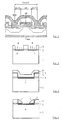
- The invention will now be described with reference to a nonlimiting embodiment example with reference to the annexed drawings wherein:
- FIG.1
- shows the structure of a power-MOS of the known art,
- FIGS.2-10
- show the different steps of a process in accordance with the invention, and
- FIG.11
- shows a power-MOS device obtained by the same process.
- An example of an embodiment of the process in accordance with the invention is explained below for the manufacture of an N-channel power-MOS. However, with the necessary modifications clear to those skilled in the art, it also applies to the case of manufacture of a P-channel power-MOS transistor.
- The process comprises in sequence the following steps. of which the initial ones, specifically from a. to d., are already provided for in the known art.
- a. Epitaxial growth of a layer of N type silicon on a N+ type silicon substrate.
- b. Growth of a layer of silicon dioxide (field oxide) on the epitaxial layer and subsequent definition of the edge of the chip by photoengraving.
- c. Formation of a
layer 2 of silicon dioxide (gate oxide) over the entire slice and subsequent deposition of alayer 3 of polycrystalline silicon (poly). - d. Photoengraving of the poly for formation of the gate.
- e. Implantation of the
region 4 with type P dopant and in particular with boron (FIG. 2). - f. Deposition of a
layer 5 of silicon nitride Si₃N₄ 20-40 nm (200-400 ångstrom) thick. - g. Deposition on the
laver 5 of silicon nitride, by a Chemical Vapor Deposition (CVD) process. of alayer 6 of silicon dioxide SiO₂ (vapox) having a thickness on the order of 500 nm (5000 ångstrom) - FIG. 3. - h. Reactive Ion Etching (RIE) of the
layer 6 of vapox dioxide so as to create aspacer 7 along the gate walls (FIG. 4). - i. Etching of the
silicon nitride layer 5 in the area not protected by the spacer. - l. Stripping of the vapox dioxide constituting the spacer to uncover the underlying silicon nitride 5 (FIG. 5).
- m. Diffusion of the dopant present in 4 with the resulting formation of the
region 8 of the body. - n. Formation of the
layers - o. Stripping of the layer of Si₃N₄ from the area previously occupied by the spacer.
- p. Implantation or predeposition of dopant, in particular arsenic, on the
area 11 previously occupied by the spacer, using as a mask thelayer 9 of silicon dioxide (FIG. 7). - q. Diffusion of the arsenic with resulting formation of the source regions 12 (FIG. 8).
- r. Stripping of the
layers - s. Deposition of a vapox layer approximately 150 nm (1500 ångstrom) thick and subsequent RIE thereof with resulting provision of a
spacer 14 along the gate walls (FIG. 8). - t. Deposition of a
layer 15 of refractory metal. in particular titanium (FIG. 9). - u. Formation on the
contact areas 16 of FIG. 10 of a silicide TiSi by Rapid Thermal Annealing (RTA). - v. Selective etching to eliminate the refractory metal covering said
spacer 14 followed by further RTA and resulting sintering of the titanium to TiSi2 (layer 16 of FIG. 10). - Indicated below are the steps, already provided in the known art, which follow: deposition of a layer of
dielectric 17 approximately 1100 nm (11000 ångstrom) thick on the front of the slice, opening of windows in the dielectric layer for formation of the source contacts, metallization on the front (layer 18 of FIG. 11) and subsequent photoengraving, passivation and further photoengraving and finally finishing of the back of the slice. - The structure of the device obtained at the end of the process is shown schematically in FIG. 11.
- Step o. of the process indicated above may be carried out later. Indeed, implantation of dopant for formation of the source regions can take place without previous stripping of the layer of Si₃N₄.
- For the photoengraving there is used photolithographic exposure equipment of the 5:1 stepper type which allows minimum apertures on the order of 1 µm with maximum misalignment between two successive photoengravings of .35 µm.
- The use of these photographic exposure units together with self-alignment techniques such as those of spacers and self-aligned silicide make it possible to obtain considerable improvements without advanced photolithographic techniques.
- In accordance with the invention the Xpitch dimension of the elementary cell is reduced to values not in excess of approximately 2-3 µm with the possibility of achieving a cell density on the order of 8·10⁷ cells per square inch (1 inch=2,54cm). As an indication Xc can be approximately 1.8 µm., and Xd about 1 µm. Indeed, the Xc dimension is conditioned by a single alignment and can fall to values of approximately 1.8 µm while Xd can fall to values of approximately 1 µm.
- The sequence of operations is simplified with a reduction of maskings from 7 to 5.
- Silicides on the source, on the body and on the gate polysilicon allow considerable reduction of the increase in parasite resistances due to the considerable reduction of the metal/semiconductor contact areas on the active regions and reduction of the increase in the resistance of the gate poly due to high integration. This also allows elimination of the risk of spikes on the aluminium of the metallization and consequently permits reduction of the body depth (not more than .4 µm) and the side dimensions of the body and gate.
- Among other advantages the RTA process makes it possible to limit the side growth or the silicide on the spacer, which would otherwise risk short circuiting the gate with the other electrodes.
- To the above advantages are to be added the following electrical advantages:
- reduction of the size of the source produces a decrease in the Ron by a factor of 2 on the low voltage devices;
- reduction of the base-emitter resistance RBE of the parasitic bipolar transistor improves the strength of the device with respect to the rapid voltage variations;
- reduction of the size of the source, which goes from the present 4-6 µm to approximately .5 µm results in an increase of the strength of the power-MOS by a factor of 10.
- Although the invention has been described for a specific embodiment it is evident that many alternatives and variations, such as in materials and dimensions, will be apparent to those skilled in the art in light of the foregoing description. For example, one of the variants can provide in step t. of the above described process the deposition of another refractory metal such as Co, W or an alloy thereof and in the latter case the formation of the related silicides in step u.
- Another variant can consist of effecting a further self-aligned ionic implantation of dopant to form a deep body P+ region between steps i. and l. described above.
Claims (6)
- Process for the manufacture of power-MOS semiconductor devices comprising the following steps:- epitaxial growth on a silicon substrate having a first conductivity type of at least one layer of silicon of the same conductivity type.- gate oxidation over the entire slice,- deposition of a layer of polycrystalline silicon on the front of the slice,- opening, by means of photolithography, of a window - hereinafter called "gate window - in the layer of polycrystalline silicon for definition of the gate polysilicon,- implantation and diffusion of dopant of a second conductivity type at the aforesaid gate window for formation of the body,- implantation and diffusion of dopant of a first conductivity type in the body for formation of the source regions,- deposition of P-Vapox dielectric on the front of the slice,- opening of windows on the front of the slice for formation of the source contacts, and- deposition of aluminium on the front of the slice to provide metallization of source and gate pads,characterized in that:- the opening of the above said gate window in the polycrystalline silicon layer is followed by:- ionic implantation of dopant of a second conductivity type into the surface of the slice at said window for formation of the body (8),- CVD deposition of a thin layer (5) of silicon nitride Si₃N₄ over the entire slice,- CVD deposition of a layer (6) of dielectric on the surface of the slice,- RIE of the layer (6) of dielectric to provide a spacer (7) along the walls of the above said gate window,- etching of the silicon nitride layer (5) in the area not protected by the spacer,- stripping of the spacer (7) so as to uncover the underlying silicon nitride,- diffusion of said implanted dopant for formation of the body region (8) and formation of layers (10,9) of silicon dioxide on the gate poly and the body respectively using Locos technology,- stripping of the nitride (5) from the area previously occupied by the spacer (7),- use of the layer (9) of silicon dioxide formed on the body as a mask for implantation or predeposition of dopant of a first conductivity type and subsequent diffusion to provide the source regions (12)- stripping of the layers (9,10) of dioxide previously formed on the body and on the gate poly,- creation of a further spacer (14) of dielectric material along the gate walls;- metallization of the source and gate contact areas by deposition of a layer (15) of refractory metal and sintering by RTA for the formation of a silicide,- selective etching for elimination of the refractory metal covering the further spacer, followed by another sintering of the silicide by RTA,- deposition of dielectric on the front of the slice and opening of windows for formation of the source contacts.
- Process for the manufacture of power-MOS semiconductor devices comprising the following steps:- epitaxial growth on a silicon substrate having a first conductivity type of at least one layer of silicon of the same conductivity type.- gate oxidation over the entire slice,- deposition of a layer of polycrystalline silicon on the front of the slice.- opening, by means of photolithography, of a window - hereinafter called "gate window" - in the layer of polycrystalline silicon for definition of the gate polysilicon,- implantation and diffusion of dopant of a second conductivity type at the aforesaid gate window for formation of the body,- implantation and diffusion of dopant of a first conductivity type in the body for formation of the source regions,- deposition of P-Vapox dielectric on the front of the slice,- opening of windows on the front of the slice for formation of the source contacts, and- deposition of aluminium on the front of the slice to provide metallization of source and gate pads,characterized in that:- the opening of the above said gate window in the polycrystalline silicon layer is followed by:- ionic implantation of dopant of a second conductivity type into the surface of the slice at said window for formation of the body (8),- CVD deposition of a thin layer (5) of silicon nitride Si₃N₄ over the entire slice,- CVD deposition of a layer (6) of dielectric on the surface of the slice,- RIE of the layer (6) of dielectric to provide a spacer (7) along the walls of the above said gate window,- etching of the silicon nitride layer (5) in the area not protected by the spacer,- stripping of the spacer (7) so as to uncover the underlying silicon nitride,- diffusion of said implanted dopant for formation of the body region (8), and formation of layers (9,10) of silicon dioxide on the gate poly and on the body respectively, using Locos technology,- use of the silicon dioxide layer (9) formed on the body as a mask for implantation of dopant of a first conductivity type through the silicon nitride layer and subsequent diffusion for provision of the source regions (12),- stripping of the nitride (5) from the area previously occupied by the spacer (7),- stripping of the layers (9,10) of dioxide previously formed on the body and on the gate poly,- creation of a further spacer (14) of dielectric material along the gate walls,- metallization of the source and gate contact areas by deposition of a layer (15) of refractory metal and formation of a silicide by sintering using RTA,- selective etching for elimination of the refractory metal covering the further spacer followed by another sintering of the silicide by RTA,- deposition of dielectric on the front of the slice and opening of windows for formation of the source contacts.
- Process in accordance with claims 1 or 2 characterized in that the etching of the silicon nitride layer (5) in the areas not protected by the spacer is followed by a second ionic implantation of dopant of a second conductivity type at the window defined by the spacer (7) for formation of a deep body region and is further followed by stripping of the spacer (7) and by the subsequent diffusion of the implanted dopant for formation of the body and deep body regions.
- Process in accordance with claims 1 or 2 characterized in that:- the silicon nitride layer (5) has a thickness between 20 and 40 nm (200 and 400 Ångstrom),- the dielectric layer (6) consists of silicon dioxide SiO₂ and has a thickness of about 500 nm (5000 Ångstrom),- creation of the spacer (14) is provided by deposition of a layer of silicon dioxide SiO₂ having a thickness of approximately 150 nm (1500 Ångstrom).
- Process in accordance with claim 1 characterized in that the photolithographic processes take place using photolithographic exposure equipment of the 5:1 stepper type.
- Process in accordance with claim 1 characterized in that for metallization of the body, source and gate contact areas there are used silicides of titanium or cobalt or tungsten or their alloys.
Applications Claiming Priority (2)
| Application Number | Priority Date | Filing Date | Title |
|---|---|---|---|
| IT02289189A IT1236994B (en) | 1989-12-29 | 1989-12-29 | PROCESS FOR THE MANUFACTURE OF POWER MOS SEMICONDUCTIVE DEVICES AND DEVICES OBTAINED WITH IT |
| IT2289189 | 1989-12-29 |
Publications (2)
| Publication Number | Publication Date |
|---|---|
| EP0435406A1 EP0435406A1 (en) | 1991-07-03 |
| EP0435406B1 true EP0435406B1 (en) | 1994-03-16 |
Family
ID=11201599
Family Applications (1)
| Application Number | Title | Priority Date | Filing Date |
|---|---|---|---|
| EP90203503A Expired - Lifetime EP0435406B1 (en) | 1989-12-29 | 1990-12-24 | Process for the manufacture of powermos semiconductor devices and the devices obtained therewith |
Country Status (6)
| Country | Link |
|---|---|
| US (1) | US5141883A (en) |
| EP (1) | EP0435406B1 (en) |
| JP (1) | JPH04305978A (en) |
| KR (1) | KR100202048B1 (en) |
| DE (1) | DE69007449T2 (en) |
| IT (1) | IT1236994B (en) |
Cited By (1)
| Publication number | Priority date | Publication date | Assignee | Title |
|---|---|---|---|---|
| DE19959346B4 (en) * | 1999-12-09 | 2004-08-26 | Micronas Gmbh | Method for producing a solid having a microstructure |
Families Citing this family (10)
| Publication number | Priority date | Publication date | Assignee | Title |
|---|---|---|---|---|
| US5288653A (en) * | 1991-02-27 | 1994-02-22 | Nec Corporation | Process of fabricating an insulated-gate field effect transistor |
| DE69434268T2 (en) * | 1994-07-14 | 2006-01-12 | Stmicroelectronics S.R.L., Agrate Brianza | Integrated structure of a high-speed MOS technologist power device and related manufacturing method |
| US5474946A (en) * | 1995-02-17 | 1995-12-12 | International Rectifier Corporation | Reduced mask process for manufacture of MOS gated devices |
| US5595918A (en) * | 1995-03-23 | 1997-01-21 | International Rectifier Corporation | Process for manufacture of P channel MOS-gated device |
| US5830798A (en) * | 1996-01-05 | 1998-11-03 | Micron Technology, Inc. | Method for forming a field effect transistor |
| KR100204805B1 (en) * | 1996-12-28 | 1999-06-15 | 윤종용 | Method for fabricating transistor |
| EP0993033A1 (en) | 1998-10-06 | 2000-04-12 | STMicroelectronics S.r.l. | Gate insulating structure for power devices, and related manufacturing process |
| US6214673B1 (en) * | 1999-07-09 | 2001-04-10 | Intersil Corporation | Process for forming vertical semiconductor device having increased source contact area |
| US7166232B2 (en) | 2000-12-21 | 2007-01-23 | Micronas Gmbh | Method for producing a solid body including a microstructure |
| ITVA20010045A1 (en) * | 2001-12-14 | 2003-06-16 | St Microelectronics Srl | PROCESS FLOW FOR THE PRODUCTION OF A VDMOS WITH SCALED AND LOW DEGREE OF BODY CHANNEL FOR HIGH DENSITY PERFORMANCE OF CORREN |
Family Cites Families (14)
| Publication number | Priority date | Publication date | Assignee | Title |
|---|---|---|---|---|
| US4443931A (en) * | 1982-06-28 | 1984-04-24 | General Electric Company | Method of fabricating a semiconductor device with a base region having a deep portion |
| US4489481A (en) * | 1982-09-20 | 1984-12-25 | Texas Instruments Incorporated | Insulator and metallization method for VLSI devices with anisotropically-etched contact holes |
| US4677735A (en) * | 1984-05-24 | 1987-07-07 | Texas Instruments Incorporated | Method of providing buried contacts for N and P channel devices in an SOI-CMOS process using a single N+polycrystalline silicon layer |
| IT1213234B (en) * | 1984-10-25 | 1989-12-14 | Sgs Thomson Microelectronics | PROCESS PERFECTED FOR THE MANUFACTURE OF DMOS SEMICONDUCTOR DEVICES. |
| EP0229362B1 (en) * | 1986-01-10 | 1993-03-17 | General Electric Company | Semiconductor device and method of fabrication |
| IT1204243B (en) * | 1986-03-06 | 1989-03-01 | Sgs Microelettronica Spa | SELF-ALIGNED PROCEDURE FOR THE MANUFACTURE OF SMALL-SIZED DMOS CELLS AND MOS DEVICES OBTAINED THROUGH THAT PROCEDURE |
| US4798810A (en) * | 1986-03-10 | 1989-01-17 | Siliconix Incorporated | Method for manufacturing a power MOS transistor |
| US4716126A (en) * | 1986-06-05 | 1987-12-29 | Siliconix Incorporated | Fabrication of double diffused metal oxide semiconductor transistor |
| US4842675A (en) * | 1986-07-07 | 1989-06-27 | Texas Instruments Incorporated | Integrated circuit isolation process |
| US4772569A (en) * | 1986-10-30 | 1988-09-20 | Mitsubishi Denki Kabushiki Kaisha | Method for forming oxide isolation films on french sidewalls |
| US4735680A (en) * | 1986-11-17 | 1988-04-05 | Yen Yung Chau | Method for the self-aligned silicide formation in IC fabrication |
| JP2604777B2 (en) * | 1988-01-18 | 1997-04-30 | 松下電工株式会社 | Manufacturing method of double diffusion type field effect semiconductor device. |
| US4949136A (en) * | 1988-06-09 | 1990-08-14 | University Of Connecticut | Submicron lightly doped field effect transistors |
| US4985740A (en) * | 1989-06-01 | 1991-01-15 | General Electric Company | Power field effect devices having low gate sheet resistance and low ohmic contact resistance |
-
1989
- 1989-12-29 IT IT02289189A patent/IT1236994B/en active IP Right Grant
-
1990
- 1990-12-24 DE DE69007449T patent/DE69007449T2/en not_active Expired - Fee Related
- 1990-12-24 US US07/632,485 patent/US5141883A/en not_active Expired - Lifetime
- 1990-12-24 EP EP90203503A patent/EP0435406B1/en not_active Expired - Lifetime
- 1990-12-28 KR KR1019900022248A patent/KR100202048B1/en not_active Expired - Fee Related
- 1990-12-28 JP JP2418101A patent/JPH04305978A/en active Pending
Non-Patent Citations (2)
| Title |
|---|
| Book "Integrated Circuit Mask Technology", 1985, pp. 160-165, Ed. Mc Graw-Hill Book Co., by D.J.Elliott * |
| Electronic Letters, Vol.25, Nr.16, 3rd August 1988, pp.1033-1034 * |
Cited By (1)
| Publication number | Priority date | Publication date | Assignee | Title |
|---|---|---|---|---|
| DE19959346B4 (en) * | 1999-12-09 | 2004-08-26 | Micronas Gmbh | Method for producing a solid having a microstructure |
Also Published As
| Publication number | Publication date |
|---|---|
| IT1236994B (en) | 1993-05-12 |
| KR100202048B1 (en) | 1999-06-15 |
| DE69007449T2 (en) | 1994-08-25 |
| EP0435406A1 (en) | 1991-07-03 |
| JPH04305978A (en) | 1992-10-28 |
| KR910013450A (en) | 1991-08-08 |
| US5141883A (en) | 1992-08-25 |
| DE69007449D1 (en) | 1994-04-21 |
| IT8922891A0 (en) | 1989-12-29 |
Similar Documents
| Publication | Publication Date | Title |
|---|---|---|
| US5231038A (en) | Method of producing field effect transistor | |
| KR100352715B1 (en) | Submicron metal gate MOS transistor and method of formation thereof | |
| JP2605008B2 (en) | Method for manufacturing semiconductor device | |
| US4384301A (en) | High performance submicron metal-oxide-semiconductor field effect transistor device structure | |
| US6852597B2 (en) | Method for fabricating power semiconductor device having trench gate structure | |
| US4102733A (en) | Two and three mask process for IGFET fabrication | |
| US5849616A (en) | Method of manufacturing a semiconductor device | |
| EP0179407B1 (en) | Method for producing a dmos semiconductor device | |
| US6252277B1 (en) | Embedded polysilicon gate MOSFET | |
| US5879994A (en) | Self-aligned method of fabricating terrace gate DMOS transistor | |
| US6261915B1 (en) | Process of making polysilicon resistor | |
| US5783474A (en) | Reduced mask process for manufacture of MOS gated devices using dopant-enhanced-oxidation of semiconductor | |
| KR19980018751A (en) | SEMICONDUCTOR DEVICE AND METHOD OF MANUFACTURING THE SAME | |
| US4985746A (en) | Semiconductor device and method of production | |
| JP2668081B2 (en) | Method of manufacturing a CMOS EPROM memory cell | |
| US4939154A (en) | Method of fabricating an insulated gate semiconductor device having a self-aligned gate | |
| EP0404372B1 (en) | Method for forming polycrystalline silicon contacts | |
| US5141883A (en) | Process for the manufacture of power-mos semiconductor devices | |
| US5234851A (en) | Small cell, low contact assistance rugged power field effect devices and method of fabrication | |
| US5225357A (en) | Low P+ contact resistance formation by double implant | |
| US4076557A (en) | Method for providing semiconductor devices | |
| US6078079A (en) | Semiconductor device and method of manufacturing the same | |
| US4621412A (en) | Manufacturing a complementary MOSFET | |
| JPH05251694A (en) | Mos type semiconductor device and its manufacture | |
| US6686276B2 (en) | Semiconductor chip having both polycide and salicide gates and methods for making same |
Legal Events
| Date | Code | Title | Description |
|---|---|---|---|
| PUAI | Public reference made under article 153(3) epc to a published international application that has entered the european phase |
Free format text: ORIGINAL CODE: 0009012 |
|
| AK | Designated contracting states |
Kind code of ref document: A1 Designated state(s): DE FR GB NL |
|
| 17P | Request for examination filed |
Effective date: 19911223 |
|
| 17Q | First examination report despatched |
Effective date: 19920512 |
|
| GRAA | (expected) grant |
Free format text: ORIGINAL CODE: 0009210 |
|
| AK | Designated contracting states |
Kind code of ref document: B1 Designated state(s): DE FR GB NL |
|
| PG25 | Lapsed in a contracting state [announced via postgrant information from national office to epo] |
Ref country code: NL Effective date: 19940316 |
|
| REF | Corresponds to: |
Ref document number: 69007449 Country of ref document: DE Date of ref document: 19940421 |
|
| ET | Fr: translation filed | ||
| NLV1 | Nl: lapsed or annulled due to failure to fulfill the requirements of art. 29p and 29m of the patents act | ||
| PLBE | No opposition filed within time limit |
Free format text: ORIGINAL CODE: 0009261 |
|
| STAA | Information on the status of an ep patent application or granted ep patent |
Free format text: STATUS: NO OPPOSITION FILED WITHIN TIME LIMIT |
|
| 26N | No opposition filed | ||
| REG | Reference to a national code |
Ref country code: FR Ref legal event code: D6 |
|
| REG | Reference to a national code |
Ref country code: GB Ref legal event code: IF02 |
|
| PGFP | Annual fee paid to national office [announced via postgrant information from national office to epo] |
Ref country code: FR Payment date: 20021210 Year of fee payment: 13 |
|
| PGFP | Annual fee paid to national office [announced via postgrant information from national office to epo] |
Ref country code: GB Payment date: 20021218 Year of fee payment: 13 |
|
| PGFP | Annual fee paid to national office [announced via postgrant information from national office to epo] |
Ref country code: DE Payment date: 20021231 Year of fee payment: 13 |
|
| PG25 | Lapsed in a contracting state [announced via postgrant information from national office to epo] |
Ref country code: GB Free format text: LAPSE BECAUSE OF NON-PAYMENT OF DUE FEES Effective date: 20031224 |
|
| PG25 | Lapsed in a contracting state [announced via postgrant information from national office to epo] |
Ref country code: DE Free format text: LAPSE BECAUSE OF NON-PAYMENT OF DUE FEES Effective date: 20040701 |
|
| GBPC | Gb: european patent ceased through non-payment of renewal fee |
Effective date: 20031224 |
|
| PG25 | Lapsed in a contracting state [announced via postgrant information from national office to epo] |
Ref country code: FR Free format text: LAPSE BECAUSE OF NON-PAYMENT OF DUE FEES Effective date: 20040831 |
|
| REG | Reference to a national code |
Ref country code: FR Ref legal event code: ST |