EP0434898A2 - Semiconductor integrated circuit - Google Patents
Semiconductor integrated circuit Download PDFInfo
- Publication number
- EP0434898A2 EP0434898A2 EP90114970A EP90114970A EP0434898A2 EP 0434898 A2 EP0434898 A2 EP 0434898A2 EP 90114970 A EP90114970 A EP 90114970A EP 90114970 A EP90114970 A EP 90114970A EP 0434898 A2 EP0434898 A2 EP 0434898A2
- Authority
- EP
- European Patent Office
- Prior art keywords
- fet
- capacitor
- resistor
- terminal
- integrated circuit
- Prior art date
- Legal status (The legal status is an assumption and is not a legal conclusion. Google has not performed a legal analysis and makes no representation as to the accuracy of the status listed.)
- Granted
Links
- 239000004065 semiconductor Substances 0.000 title claims abstract description 27
- 239000003990 capacitor Substances 0.000 claims abstract description 77
- 238000007599 discharging Methods 0.000 description 6
- 238000010586 diagram Methods 0.000 description 4
- 230000000694 effects Effects 0.000 description 4
- 238000010276 construction Methods 0.000 description 1
- 230000006378 damage Effects 0.000 description 1
- 230000005669 field effect Effects 0.000 description 1
- 238000012986 modification Methods 0.000 description 1
- 230000004048 modification Effects 0.000 description 1
- 230000010355 oscillation Effects 0.000 description 1
Images


Classifications
-
- H—ELECTRICITY
- H01—ELECTRIC ELEMENTS
- H01P—WAVEGUIDES; RESONATORS, LINES, OR OTHER DEVICES OF THE WAVEGUIDE TYPE
- H01P1/00—Auxiliary devices
- H01P1/10—Auxiliary devices for switching or interrupting
- H01P1/15—Auxiliary devices for switching or interrupting by semiconductor devices
Definitions
- the present invention relates to a semiconductor integrated circuit, and more particularly, to a semiconductor integrated circuit for a high frequency band such as a microwave band.
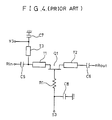
- Figure 4 shows a conventional semiconductor integrated circuit.
- reference numeral Q1 designates a field effect transistor (referred to as an FET hereinafter) and reference numerals T1 and T2 designate microwave lines connected to a source and a drain of the FETQ1, respectively.
- Reference numerals C5 and C6 designate capacitors connected to the microwave lines T1 and T2, respectively.
- Reference numeral R1 designates a resistor connected to a gate of the FETQ1
- reference numeral C8 designates a capacitor connected to the resistor R1
- reference numeral T3 designates a 1/4 wavelength line connected to the microwave line T1 and the capacitor C5
- reference numeral C7 designates a capacitor connected to the microwave line T3.
- a drive signal input terminal S3 connected to a connecting point between the resistor R1 and the capacitor C8 is used to perform switching operation of the FETQ1.
- the 1/4 wavelength line T3 and the capacitor C7 serve as a circuit for source voltage bias of the FETQ1, which source voltage bias of the FETQ1 is applied from a power supply terminal V3 connected to a connecting point between the 1/4 wavelength line T3 and the capacitor C7.
- a high frequency signal is input from Rin and output to Rout.
- the drive signal input terminal S3 becomes high the FETQ1 is turned ON and the high frequency signal input from the Rin is output to the Rout.
- the drive signal input terminal S3 becomes low the FETQ1 is turned OFF and the high frequency signal input from the Rin is not output to the Rout.
- the resistor R1 is generally set sufficiently higher than line impedance of the microwave lines T1 and T2. Therefore, when the FETQ1 is ON, the high frequency signal is prevented from being leaked to the gate side of the FETQ1 by capacitance Cgs between the gate and source of the FETQ1. In addition, when mutual conductance Gm of the FETQ1 is fairly high, oscillation can be prevented. Furthermore, electrostatic destruction of the gate of the FETQ1 can be prevented.
- the capacitor C8 and the resistor R1 serve as a RC low-pass filter circuit in which capacitance of the capacitor C8 is set at a large value so as to be sufficiently low impedance to the high frequency signal so that the high frequency signal may not be leaked from the input terminal S3.
- the resistor R1 is used in the example shown in figure 4, a 1/4 wavelength line is sometimes used instead of the resistor R1.
- the present invention was made to solve the above problem and it is an object of the present invention to provide a semiconductor integrated circuit in which power consumption is reduced and a gate of an FETQ1 can be driven at high speed because charging and discharging of a capacitor C8 is dispensed with.
- a semiconductor integrated circuit in accordance with the present invention comprises a first FET serving as a transfer gate controlling transfer of a high frequency signal, a first and a second capacitors connected to a gate of the first FET directly or through a resistor or a 1/4 wavelength line, a second FET having its drain connected to the first capacitor and its source grounded at a high frequency band, and a third FET having its drain connected to the second capacitor and its source grounded at a high frequency band.
- a semiconductor integrated circuit in accordance with the present invention further comprises a second resistor connected to the first capacitor in parallel, a third resistor connected to the second capacitor in parallel and a fourth resistor having one end connected to a connecting point between the second resistor and the third resistor and the other end fixed to a certain potential.
- the first capacitor transfers the high frequency signal by the second FET when the first FET is ON and the second capacitor transfers the high frequency signal by the third FET when the first FET is OFF, so that the high frequency signal is grounded at a high frequency band through the first capacitor or the second capacitor in both cases where the first FET is ON and OFF. Therefore, the first and second capacitors play the same role as the capacitor C8 in the prior art.
- this invention is different from the prior art in that the first and second capacitors are electrically made to be a floating state by the second and third FET's in accordance with the ON or OFF state of the first FET, so that charging and discharging of the capacitor is dispensed with. As a result, power consumption is reduced and the gate of the first FET can be driven at a high speed because there is no delay due to charging and discharging of the capacitor.
- the second, third and fourth resistors are further provided, a potential necessary for the gate of the first FET to be driven can be generated by those resistors.
- Figure 1 shows a semiconductor integrated circuit in accordance with a first embodiment of the present invention.
- reference numeral Q1 designates a first FET serving as a transfer gate controlling transfer of a high frequency signal
- reference numerals T1 and T2 designate microwave lines connected to a source and a drain of the FETQ1, respectively.
- Reference numerals C5 and C6 designate DC cutting capacitors
- references Rin and Rout designate microwave input/output terminals through which a high frequency signal such as a microwave signal is input or output
- reference numeral T3 designates a 1/4 wavelength line serving as a part of a source bias circuit of the FETQ1.
- Reference numeral C7 designates a capacitor for grounding the high frequency signal, which also serves as a part of the source bias circuit of the FETQ1 together with the microwave line T1
- reference numeral V3 designates a power supply terminal for source bias of the FETQ1
- reference numerals C1 and C2 designate a first and a second capacitors connected to a gate of the FETQ1 through a resistor R1, respectively.
- Reference numeral Q2 designates a second FET having its drain connected to the capacitor C1 and its source grounded through the capacitor C3
- reference numeral Q3 designates a third FET having its drain connected to the capacitor C2 and its source grounded through the capacitor C4
- reference numerals S1 and S2 designate drive signal input terminals connected to the gates of the second and third FET's Q2 and Q3, respectively.
- Reference numeral S3 designates a drive signal input terminal connected to a connecting point between the first and second capacitors C1 and C2 and the resistor R1
- reference numerals V1 and V2 designate power supply terminals for source bias of the second and third FET's Q2 and Q3, respectively.
- Figure 2 shows an example of an input waveform of a drive signal in each of the drive signal input terminals S1 to S3 with time shown by the abscissa.
- a power supply terminal V3 is grounded (0V) in a DC manner, a source potential of the FETQ1 is 0V and a pinch off (cut-off) voltage of the FETQ1 is Vp.
- the FET is a normally ON type and when a voltage of -Vp is applied between the gate and source thereof, the FET is turned OFF.
- the FETQ1 performs ON/OFF switching operation and then an output waveform shown in figure 2 is obtained from the microwave output terminal Rout corresponding to the switching operation of the FETQ1.
- a potential of the power supply terminal V1 is set at 0V and a signal is input from the terminal S1, which signal rises, reaches 0v and falls while an input voltage of the terminal S3 is 0v, and it is at -Vp while the input voltage of the terminal S3 is -Vp as shown in figure 2.
- the FETQ2 is turned ON. In this ON state, an electric charge amount Q c1 , which corresponds to a potential difference V c1 between the terminals S3 and V1, is stored in the capacitor C1.
- a potential of the power supply terminal V2 is set at -Vp and a signal is input from the terminal S2, which signal rises, reaches -Vp and falls while the input voltage of the terminal S3 is -Vp and it is at -2Vp while the input voltage of the terminal S3 is 0V as shown in figure 2.
- the FETQ3 is turned ON. Therefore, at this time, the electric charge amount Q c2 , which corresponds to a potential difference between the terminals S3 and V2, is stored in the capacitor C2. In this embodiment, if there is no voltage fall at the FETQ3, a voltage across the capacitor is 0V.
- the capacitors C1 and C2 are made to electrically be in a floating state by the FET's Q2 and Q3, respectively in accordance with ON or OFF state of the FETQ1 in which they are electrically insulated from the outside so that an electric charge may not flow into them. Therefore, voltages across the capacitors C1 and C2 can be always constant (0V in this embodiment). As a result, power consumption can be reduced because charging or discharging of the capacitor can be dispensed with. In addition, there is no delay of time due to charging or discharging of the capacitor, thereby the FETQ1 can be driven at high speed.
- the FETQ1 can be used as an attenuator or an amplifier when it is turned ON or OFF in a halfway manner. Furthermore, it can be used as a gate grounded type impedance converter by applying a bias circuit to the drain of the FETQ1.
- Figure 3 shows a semiconductor integrated circuit in accordance with a second embodiment of the present invention.
- the same references as in figure 1 designate the same part.
- Reference numerals R2 and R3 designate a second and a third resistors connected to the first capacitor C1 and the second capacitor C2 in parallel, respectively.
- Reference numeral R4 designates a fourth resistor for grounding a connecting point between the first and second capacitors C1 and C2 and the resistor R1.
- a potential of a node S3 is determined by values of the resistors R2 and R4 when the FETQ2 is ON.
- a potential of the power supply terminal V1 is 0V
- a potential of the terminal S3 is 0V.
- a potential of the node S3 is determined by values of the resistors R3 and R4. For example, when a potential of the power supply terminal V2 is -Vp, a potential of the terminal S3 is as follows; -Vp ⁇ R4 / ( R3 + R4) If the value of the resistor R4 is set so as to be considerably larger than that of the resistor R3, a potential of the terminal S3 can be almost equal to -Vp.
- an input signal necessary for the node S3 can be composed from the input signal to the drive signal input terminals S1 and S2.
- this is not necessarily a grounding potential and may be a fixed potential determined by correlation between the input voltages to the terminals S1, S2, V1, V2 and V3.
- the resistor R1 is provided so that impedance may be considerably higher than the line impedance of the microwave lines T1 and T2 in the above embodiment, the resistor R1 can be dispensed with and they may be directly connected if considerably high impedance can be obtained.
- the 1/4 wavelength line, or the resistor and the 1/4 wavelength line which are connected in series may be provided.
- the input signal to the terminal S1 is set such that it rises, reaches 0V and falls while the input voltage of the terminal S3 is 0V and it is -Vp while the input voltage of the terminal S3 is -Vp.
- the input signal to the terminal S2 is set such that it rises, reaches -Vp and falls while the input voltage of the terminal S3 is -Vp and it is -2Vp while the input voltage of the terminal S3 is 0V.
- the input signal to the terminal S1 may be set such that it is 0v while the input voltage of the terminal S3 is 0V and it is -Vp while the input voltage of the terminal S3 is Vp and the input signal to the terminal S2 may be set such that it is -Vp while the input voltage of the terminal S3 is -Vp and it is -2Vp while the input voltage of the terminal S3 is 0V.
- the gate of the FETQ1 can be always grounded by either capacitor C1 or C2 at a high frequency band through the resistor R1 even when the input voltage rises or falls.
- potentials of the power supply terminals V1, V2 and V3 are set at 0V, -Vp and 0V, respectively in the above embodiments, these can be set at any value if the FET's Q1, Q2 and Q3 operate.
- the FETQ1 serves as a transfer gate for controlling transfer of a high frequency signal even without the FET's T1 to T3 and capacitors C1 to C7.
- a semiconductor integrated circuit in accordance with the present invention comprises a first FET serving as a transfer gate controlling transfer of a high frequency signal, a first and a second capacitors connected to a gate of the first FET directly or through a resistor or a 1/4 wavelength line, a second FET having its drain connected to the first capacitor and its source grounded at a high frequency band and a third FET having its drain connected to the second capacitor and its source grounded at a high frequency band. Therefore, the first and second capacitors can be electrically in a floating state by the second and third FET's, respectively in accordance with ON or OFF state of the first FET. As a result, power consumption is reduced and there is no delay of time because charging or discharging of the capacitor can be dispensed with, whereby the first FET can be driven at high speed.
- a semiconductor integrated circuit in accordance with the present invention comprises a second resistor connected to the first capacitor in parallel, a third resistor connected to the second capacitor in parallel, a fourth resistor having one end connected to a connecting point between the second resistor and the third resistor and the other end fixed to a certain potential. Therefore, in addition to the above effect, there can be provided a high frequency semiconductor integrated circuit with high performance in which a potential required when the first FET is driven can be provided by these resistors and a signal necessary for gate driving can be easily provided.
Abstract
Description
- The present invention relates to a semiconductor integrated circuit, and more particularly, to a semiconductor integrated circuit for a high frequency band such as a microwave band.
- Figure 4 shows a conventional semiconductor integrated circuit. In figure 4, reference numeral Q1 designates a field effect transistor (referred to as an FET hereinafter) and reference numerals T1 and T2 designate microwave lines connected to a source and a drain of the FETQ1, respectively. Reference numerals C5 and C6 designate capacitors connected to the microwave lines T1 and T2, respectively. Reference numeral R1 designates a resistor connected to a gate of the FETQ1, reference numeral C8 designates a capacitor connected to the resistor R1, reference numeral T3 designates a 1/4 wavelength line connected to the microwave line T1 and the capacitor C5, and reference numeral C7 designates a capacitor connected to the microwave line T3.
- Next, operation thereof will be described. A drive signal input terminal S3 connected to a connecting point between the resistor R1 and the capacitor C8 is used to perform switching operation of the FETQ1. In addition, the 1/4 wavelength line T3 and the capacitor C7 serve as a circuit for source voltage bias of the FETQ1, which source voltage bias of the FETQ1 is applied from a power supply terminal V3 connected to a connecting point between the 1/4 wavelength line T3 and the capacitor C7. A high frequency signal is input from Rin and output to Rout. When the drive signal input terminal S3 becomes high, the FETQ1 is turned ON and the high frequency signal input from the Rin is output to the Rout. When the drive signal input terminal S3 becomes low, the FETQ1 is turned OFF and the high frequency signal input from the Rin is not output to the Rout.
- The resistor R1 is generally set sufficiently higher than line impedance of the microwave lines T1 and T2. Therefore, when the FETQ1 is ON, the high frequency signal is prevented from being leaked to the gate side of the FETQ1 by capacitance Cgs between the gate and source of the FETQ1. In addition, when mutual conductance Gm of the FETQ1 is fairly high, oscillation can be prevented. Furthermore, electrostatic destruction of the gate of the FETQ1 can be prevented.
- The capacitor C8 and the resistor R1 serve as a RC low-pass filter circuit in which capacitance of the capacitor C8 is set at a large value so as to be sufficiently low impedance to the high frequency signal so that the high frequency signal may not be leaked from the input terminal S3. In addition, although the resistor R1 is used in the example shown in figure 4, a 1/4 wavelength line is sometimes used instead of the resistor R1.
- Since the conventional semiconductor integrated circuit is structured as described above, a considerably large drive circuit such as a TTL circuit is required in order to control a potential of the drive signal input terminal S3, to drive the capacitor C8 and the gate of the FETQ1, with the result that power consumption is increased and a switching speed of the FETQ1 is slow because it is necessary to charge and discharge the capacitor C8.
- The present invention was made to solve the above problem and it is an object of the present invention to provide a semiconductor integrated circuit in which power consumption is reduced and a gate of an FETQ1 can be driven at high speed because charging and discharging of a capacitor C8 is dispensed with.
- It is another object of the present invention to provide a semiconductor integrated circuit in which a signal for gate driving can be easily obtained by generating the same inside the integrated circuit.
- Other objects and advantages of the present invention will become apparent from the detailed description given hereinafter; it should be understood, however, that the detailed description and specific embodiment are given by way of illustration only, since various changes and modifications within the spirit and scope of the invention will become apparent to those skilled in the art from this detailed description.
- A semiconductor integrated circuit in accordance with the present invention comprises a first FET serving as a transfer gate controlling transfer of a high frequency signal, a first and a second capacitors connected to a gate of the first FET directly or through a resistor or a 1/4 wavelength line, a second FET having its drain connected to the first capacitor and its source grounded at a high frequency band, and a third FET having its drain connected to the second capacitor and its source grounded at a high frequency band.
- A semiconductor integrated circuit in accordance with the present invention further comprises a second resistor connected to the first capacitor in parallel, a third resistor connected to the second capacitor in parallel and a fourth resistor having one end connected to a connecting point between the second resistor and the third resistor and the other end fixed to a certain potential.
- According to the present invention, the first capacitor transfers the high frequency signal by the second FET when the first FET is ON and the second capacitor transfers the high frequency signal by the third FET when the first FET is OFF, so that the high frequency signal is grounded at a high frequency band through the first capacitor or the second capacitor in both cases where the first FET is ON and OFF. Therefore, the first and second capacitors play the same role as the capacitor C8 in the prior art. However, this invention is different from the prior art in that the first and second capacitors are electrically made to be a floating state by the second and third FET's in accordance with the ON or OFF state of the first FET, so that charging and discharging of the capacitor is dispensed with. As a result, power consumption is reduced and the gate of the first FET can be driven at a high speed because there is no delay due to charging and discharging of the capacitor.
- In addition, according to the present invention, since the second, third and fourth resistors are further provided, a potential necessary for the gate of the first FET to be driven can be generated by those resistors.
-
- Figure 1 is a diagram showing a semiconductor integrated circuit in accordance with a first embodiment of the present invention;
- Figure 2 is a diagram showing an input voltage waveform to each terminal of the semiconductor integrated circuit shown in figure 1;
- Figure 3 is a diagram showing a semiconductor integrated circuit in accordance with a second embodiment of the present invention; and
- Figure 4 is a diagram showing a conventional semiconductor integrated circuit.
- An embodiment of the present invention will be described in detail in reference to drawings.
- Figure 1 shows a semiconductor integrated circuit in accordance with a first embodiment of the present invention. In figure 1, reference numeral Q1 designates a first FET serving as a transfer gate controlling transfer of a high frequency signal, and reference numerals T1 and T2 designate microwave lines connected to a source and a drain of the FETQ1, respectively. Reference numerals C5 and C6 designate DC cutting capacitors, references Rin and Rout designate microwave input/output terminals through which a high frequency signal such as a microwave signal is input or output, and reference numeral T3 designates a 1/4 wavelength line serving as a part of a source bias circuit of the FETQ1. Reference numeral C7 designates a capacitor for grounding the high frequency signal, which also serves as a part of the source bias circuit of the FETQ1 together with the microwave line T1, reference numeral V3 designates a power supply terminal for source bias of the FETQ1, and reference numerals C1 and C2 designate a first and a second capacitors connected to a gate of the FETQ1 through a resistor R1, respectively. Reference numeral Q2 designates a second FET having its drain connected to the capacitor C1 and its source grounded through the capacitor C3, reference numeral Q3 designates a third FET having its drain connected to the capacitor C2 and its source grounded through the capacitor C4, and reference numerals S1 and S2 designate drive signal input terminals connected to the gates of the second and third FET's Q2 and Q3, respectively. Reference numeral S3 designates a drive signal input terminal connected to a connecting point between the first and second capacitors C1 and C2 and the resistor R1, reference numerals V1 and V2 designate power supply terminals for source bias of the second and third FET's Q2 and Q3, respectively.
- Then, operation thereof will be described.
- Figure 2 shows an example of an input waveform of a drive signal in each of the drive signal input terminals S1 to S3 with time shown by the abscissa.
- It is assumed that a power supply terminal V3 is grounded (0V) in a DC manner, a source potential of the FETQ1 is 0V and a pinch off (cut-off) voltage of the FETQ1 is Vp. In addition, it is assumed that the FET is a normally ON type and when a voltage of -Vp is applied between the gate and source thereof, the FET is turned OFF.
- At this time, as shown in figure 2, if the drive signal input to the terminal S3 is set at 0v at high level and -Vp at low level, the FETQ1 performs ON/OFF switching operation and then an output waveform shown in figure 2 is obtained from the microwave output terminal Rout corresponding to the switching operation of the FETQ1.
- Then, a potential of the power supply terminal V1 is set at 0V and a signal is input from the terminal S1, which signal rises, reaches 0v and falls while an input voltage of the terminal S3 is 0v, and it is at -Vp while the input voltage of the terminal S3 is -Vp as shown in figure 2. At this time, only when 0V is input to the terminal S1 and the terminal S3 and the terminal V1 become the same potential of 0v, the FETQ2 is turned ON. In this ON state, an electric charge amount Qc1, which corresponds to a potential difference Vc1 between the terminals S3 and V1, is stored in the capacitor C1. More specifically, if capacitance of the capacitor C1 is Cc1, the electric charge amount Qc1 is as follows:

In this embodiment, if there is no voltage fall at the FETQ2, the voltage Vc1 across the capacitor C1 can be always 0V. - In addition, when the input voltage of the terminal S1 becomes -Vp, the FETQ2 is turned OFF, so that the electric charge amount Qc1 is stored in the capacitor C1 as it is. As a result, a potential across the capacitor C1 is always kept at a constant value.
- When the input voltages of the terminal S1 and the terminal S3 become 0V again, the FETQ2 is turned ON as described above, but storage of an electric charge does not happen because the electric charge amount Qc1 is already stored in the capacitor C1 and both ends of the capacitor C1 are at the same potential.
- Then, a potential of the power supply terminal V2 is set at -Vp and a signal is input from the terminal S2, which signal rises, reaches -Vp and falls while the input voltage of the terminal S3 is -Vp and it is at -2Vp while the input voltage of the terminal S3 is 0V as shown in figure 2. Thus, only when the terminal S3 and the terminal V2 are at the same potential of -Vp, the FETQ3 is turned ON. Therefore, at this time, the electric charge amount Qc2, which corresponds to a potential difference between the terminals S3 and V2, is stored in the capacitor C2. In this embodiment, if there is no voltage fall at the FETQ3, a voltage across the capacitor is 0V.
- When the input voltage of the terminal S2 becomes -2Vp, the FETQ3 is turned OFF, so that the electric charge amount Qc2 is stored in the capacitor C2 as it is. As a result, both ends of the capacitor C2 is always kept at a constant value. Then, when the input potential of the terminal S2 becomes -Vp again, the FETQ3 is turned ON. However, since the electric charge amount Qc2 is already stored in the capacitor C2, both ends of the capacitor C2 become the same potential, so that store of an electric charge into the capacitor C2 does not arise.
- Therefore, since either FETQ2 or FETQ3 can be turned ON except when the input voltage of the terminal S3 rises or falls in this construction, the gate of the FETQ1 can be always grounded (except when it rises or falls) at a high frequency band by the capacitor C1 or C2 through the resistor R1. As a result, the same effect as in the conventional circuit shown in figure 4 can be obtained.
- In addition, as described above, the capacitors C1 and C2 are made to electrically be in a floating state by the FET's Q2 and Q3, respectively in accordance with ON or OFF state of the FETQ1 in which they are electrically insulated from the outside so that an electric charge may not flow into them. Therefore, voltages across the capacitors C1 and C2 can be always constant (0V in this embodiment). As a result, power consumption can be reduced because charging or discharging of the capacitor can be dispensed with. In addition, there is no delay of time due to charging or discharging of the capacitor, thereby the FETQ1 can be driven at high speed.
- As described above, a switching circuit with high performance for a high frequency band can be implemented by using the thus constructed semiconductor integrated circuit. In addition, the FETQ1 can be used as an attenuator or an amplifier when it is turned ON or OFF in a halfway manner. Furthermore, it can be used as a gate grounded type impedance converter by applying a bias circuit to the drain of the FETQ1.
- Figure 3 shows a semiconductor integrated circuit in accordance with a second embodiment of the present invention. In figure 2, the same references as in figure 1 designate the same part. Reference numerals R2 and R3 designate a second and a third resistors connected to the first capacitor C1 and the second capacitor C2 in parallel, respectively. Reference numeral R4 designates a fourth resistor for grounding a connecting point between the first and second capacitors C1 and C2 and the resistor R1.
- Then, operation thereof will be described.
- When a signal voltage shown in figure 2 is input to the drive signal input terminals S1 and S2, a potential of a node S3 is determined by values of the resistors R2 and R4 when the FETQ2 is ON. When a potential of the power supply terminal V1 is 0V, a potential of the terminal S3 is 0V.
- When the FETQ2 is OFF, a potential of the node S3 is determined by values of the resistors R3 and R4. For example, when a potential of the power supply terminal V2 is -Vp, a potential of the terminal S3 is as follows;
-Vp · R4 / ( R3 + R4)
If the value of the resistor R4 is set so as to be considerably larger than that of the resistor R3, a potential of the terminal S3 can be almost equal to -Vp. - Therefore, an input signal necessary for the node S3 can be composed from the input signal to the drive signal input terminals S1 and S2.
- Although the connecting point between the capacitors C1 and C2 and the resistor R1 is grounded through the resistor R4 in the above embodiment, this is not necessarily a grounding potential and may be a fixed potential determined by correlation between the input voltages to the terminals S1, S2, V1, V2 and V3.
- In addition, although the resistor R1 is provided so that impedance may be considerably higher than the line impedance of the microwave lines T1 and T2 in the above embodiment, the resistor R1 can be dispensed with and they may be directly connected if considerably high impedance can be obtained. In addition, instead of the resistor, the 1/4 wavelength line, or the resistor and the 1/4 wavelength line which are connected in series, may be provided.
- Although the normally ON type FET is used in the above embodiment, the same effect can be obtained even when a normally OFF type FET is used.
- In addition, in the above embodiment, as shown in figure 2, the input signal to the terminal S1 is set such that it rises, reaches 0V and falls while the input voltage of the terminal S3 is 0V and it is -Vp while the input voltage of the terminal S3 is -Vp. Furthermore, the input signal to the terminal S2 is set such that it rises, reaches -Vp and falls while the input voltage of the terminal S3 is -Vp and it is -2Vp while the input voltage of the terminal S3 is 0V. However, the input signal to the terminal S1 may be set such that it is 0v while the input voltage of the terminal S3 is 0V and it is -Vp while the input voltage of the terminal S3 is Vp and the input signal to the terminal S2 may be set such that it is -Vp while the input voltage of the terminal S3 is -Vp and it is -2Vp while the input voltage of the terminal S3 is 0V. In this case, the gate of the FETQ1 can be always grounded by either capacitor C1 or C2 at a high frequency band through the resistor R1 even when the input voltage rises or falls.
- In addition, although potentials of the power supply terminals V1, V2 and V3 are set at 0V, -Vp and 0V, respectively in the above embodiments, these can be set at any value if the FET's Q1, Q2 and Q3 operate.
- Although a description is given of the microwave circuit using the microwave line in the above embodiments, it is needless to say that the same effect can be obtained if the FETQ1 serves as a transfer gate for controlling transfer of a high frequency signal even without the FET's T1 to T3 and capacitors C1 to C7.
- As described above, a semiconductor integrated circuit in accordance with the present invention comprises a first FET serving as a transfer gate controlling transfer of a high frequency signal, a first and a second capacitors connected to a gate of the first FET directly or through a resistor or a 1/4 wavelength line, a second FET having its drain connected to the first capacitor and its source grounded at a high frequency band and a third FET having its drain connected to the second capacitor and its source grounded at a high frequency band. Therefore, the first and second capacitors can be electrically in a floating state by the second and third FET's, respectively in accordance with ON or OFF state of the first FET. As a result, power consumption is reduced and there is no delay of time because charging or discharging of the capacitor can be dispensed with, whereby the first FET can be driven at high speed.
- Furthermore, a semiconductor integrated circuit in accordance with the present invention comprises a second resistor connected to the first capacitor in parallel, a third resistor connected to the second capacitor in parallel, a fourth resistor having one end connected to a connecting point between the second resistor and the third resistor and the other end fixed to a certain potential. Therefore, in addition to the above effect, there can be provided a high frequency semiconductor integrated circuit with high performance in which a potential required when the first FET is driven can be provided by these resistors and a signal necessary for gate driving can be easily provided.
- Although the present invention has been described and illustrated in detail, it is clearly understood that the same is by way of illustration and example only and is not to be taken by way of limitation, the spirit and scope of the present invention being limited only by the terms of the appended claims.
Claims (6)
- A semiconductor integrated circuit, characterized by
a first FET (Q1) serving as a transfer gate controlling transfer of a high frequency signal;
a first and a second capacitors (C1,C2) connected to a gate of said first FET (Q1) directly or through a resistor (R1) or a 1/4 wavelength line;
a second FET (Q2) having its drain connected to said first capacitor (C1) and its source grounded at a high frequency band; and
a third FET (Q3) having its drain connected to said second capacitor (C2) and its source grounded at a high frequency band. - A semiconductor integrated circuit as claimed in claim 1, further characterized by
a second resistor (R2) connected to said first capacitor (C1) in parallel;
a third resistor (R3) connected to said second capacitor (C2) in parallel; and
a fourth resistor (R4) having one end connected to a connecting point (S3) between said second and third resistors (R2, R3) and the other end fixed to a certain potential. - A semiconductor integrated circuit as claimed in claims 1 or 2, characterized in that said first FET (Q1) comprises a normally ON type FET or normally OFF type FET.
- A semiconductor integrated circuit as claimed in one of the claims 1 to 3, characterized in that a drain terminal of said first FET (Q1) is connected to a microwave output terminal (Rout) through a microwave line (T2) and a source terminal of said first FET (Q1) is connected to a microwave input terminal (Rin) through the microwave line (T1).
- A semiconductor integrated circuit as claimed in claim 4, characterized by DC cutting capacitors (C6, C5) between said microwave line (T2) and said microwave output terminal (Rout) an between said microwave line (T1) and the microwave input terminal (Rin).
- A semiconductor integrated circuit as claimed in claims 4 or 5, characterized in that a source terminal of said first FET (Q1) is connected to a source bias circuit (T3, C7).
Applications Claiming Priority (2)
| Application Number | Priority Date | Filing Date | Title |
|---|---|---|---|
| JP342766/89 | 1989-12-28 | ||
| JP1342766A JPH0773202B2 (en) | 1989-12-28 | 1989-12-28 | Semiconductor integrated circuit |
Publications (3)
| Publication Number | Publication Date |
|---|---|
| EP0434898A2 true EP0434898A2 (en) | 1991-07-03 |
| EP0434898A3 EP0434898A3 (en) | 1992-02-26 |
| EP0434898B1 EP0434898B1 (en) | 1996-03-27 |
Family
ID=18356334
Family Applications (1)
| Application Number | Title | Priority Date | Filing Date |
|---|---|---|---|
| EP90114970A Expired - Lifetime EP0434898B1 (en) | 1989-12-28 | 1990-08-03 | Semiconductor integrated circuit |
Country Status (4)
| Country | Link |
|---|---|
| US (1) | US5072142A (en) |
| EP (1) | EP0434898B1 (en) |
| JP (1) | JPH0773202B2 (en) |
| DE (1) | DE69026226T2 (en) |
Cited By (1)
| Publication number | Priority date | Publication date | Assignee | Title |
|---|---|---|---|---|
| EP0723337A2 (en) * | 1995-01-23 | 1996-07-24 | Sony Corporation | Switching circuit and composite arrangement |
Families Citing this family (8)
| Publication number | Priority date | Publication date | Assignee | Title |
|---|---|---|---|---|
| DE69318879T2 (en) * | 1992-04-03 | 1998-10-08 | Matsushita Electric Ind Co Ltd | Ceramic multi-layer substrate for high frequencies |
| US5903178A (en) * | 1994-12-16 | 1999-05-11 | Matsushita Electronics Corporation | Semiconductor integrated circuit |
| US6396325B2 (en) * | 1999-12-03 | 2002-05-28 | Fairchild Semiconductor Corporation | High frequency MOSFET switch |
| US6897704B2 (en) * | 2001-05-25 | 2005-05-24 | Thunder Creative Technologies, Inc. | Electronic isolator |
| US20040196089A1 (en) * | 2003-04-02 | 2004-10-07 | O'donnell John J. | Switching device |
| ES2263357B1 (en) * | 2004-11-16 | 2007-11-16 | Diseño De Sistemas En Silicio, S.A. | SWITCHING CIRCUIT FOR OBTAINING A DUPLICATED DYNAMIC RANGE. |
| DE102005027426B4 (en) * | 2005-06-14 | 2008-12-11 | Rohde & Schwarz Gmbh & Co. Kg | Electronic high frequency switch with gallium arsenide field effect transistor |
| JP6428341B2 (en) | 2015-02-13 | 2018-11-28 | 三菱電機株式会社 | Frequency multiplier |
Citations (4)
| Publication number | Priority date | Publication date | Assignee | Title |
|---|---|---|---|---|
| US3665320A (en) * | 1969-07-11 | 1972-05-23 | Sony Corp | Gate circuit |
| US3902078A (en) * | 1974-04-01 | 1975-08-26 | Crystal Ind Inc | Analog switch |
| FR2346909A1 (en) * | 1973-05-08 | 1977-10-28 | Thomson Csf | IMPROVEMENTS TO ANALOGUE DOORS |
| FR2607643A1 (en) * | 1986-11-28 | 1988-06-03 | Mitsubishi Electric Corp | MICROWAVE SEMICONDUCTOR SWITCH |
Family Cites Families (5)
| Publication number | Priority date | Publication date | Assignee | Title |
|---|---|---|---|---|
| US4728826A (en) * | 1986-03-19 | 1988-03-01 | Siemens Aktiengesellschaft | MOSFET switch with inductive load |
| FR2612018B1 (en) * | 1987-03-06 | 1989-05-26 | Labo Electronique Physique | HYPERFREQUENCY MIXER |
| US4908531A (en) * | 1988-09-19 | 1990-03-13 | Pacific Monolithics | Monolithic active isolator |
| US4873460A (en) * | 1988-11-16 | 1989-10-10 | California Institute Of Technology | Monolithic transistor gate energy recovery system |
| US4939485A (en) * | 1988-12-09 | 1990-07-03 | Varian Associates, Inc. | Microwave field effect switch |
-
1989
- 1989-12-28 JP JP1342766A patent/JPH0773202B2/en not_active Expired - Lifetime
-
1990
- 1990-08-02 US US07/561,977 patent/US5072142A/en not_active Expired - Fee Related
- 1990-08-03 DE DE69026226T patent/DE69026226T2/en not_active Expired - Fee Related
- 1990-08-03 EP EP90114970A patent/EP0434898B1/en not_active Expired - Lifetime
Patent Citations (4)
| Publication number | Priority date | Publication date | Assignee | Title |
|---|---|---|---|---|
| US3665320A (en) * | 1969-07-11 | 1972-05-23 | Sony Corp | Gate circuit |
| FR2346909A1 (en) * | 1973-05-08 | 1977-10-28 | Thomson Csf | IMPROVEMENTS TO ANALOGUE DOORS |
| US3902078A (en) * | 1974-04-01 | 1975-08-26 | Crystal Ind Inc | Analog switch |
| FR2607643A1 (en) * | 1986-11-28 | 1988-06-03 | Mitsubishi Electric Corp | MICROWAVE SEMICONDUCTOR SWITCH |
Cited By (3)
| Publication number | Priority date | Publication date | Assignee | Title |
|---|---|---|---|---|
| EP0723337A2 (en) * | 1995-01-23 | 1996-07-24 | Sony Corporation | Switching circuit and composite arrangement |
| EP0723337A3 (en) * | 1995-01-23 | 1997-04-23 | Sony Corp | Switching circuit and composite arrangement |
| US5717356A (en) * | 1995-01-23 | 1998-02-10 | Sony Corporation | Low insertion loss switch |
Also Published As
| Publication number | Publication date |
|---|---|
| DE69026226T2 (en) | 1996-10-10 |
| JPH0773202B2 (en) | 1995-08-02 |
| US5072142A (en) | 1991-12-10 |
| EP0434898B1 (en) | 1996-03-27 |
| EP0434898A3 (en) | 1992-02-26 |
| DE69026226D1 (en) | 1996-05-02 |
| JPH03201801A (en) | 1991-09-03 |
Similar Documents
| Publication | Publication Date | Title |
|---|---|---|
| US4151425A (en) | Voltage sequencing circuit for sequencing voltages to an electrical device | |
| US4542310A (en) | CMOS bootstrapped pull up circuit | |
| EP0110130B1 (en) | Circuit producing an output free from a leakage between output and input ends | |
| EP0231204B1 (en) | Back bias generator | |
| JPS6260311A (en) | Voltage switching device | |
| US4398100A (en) | Booster circuit | |
| US4255715A (en) | Offset correction circuit for differential amplifiers | |
| EP0404124B1 (en) | Charge pump having pull-up circuit operating with two clock pulse sequences | |
| US4680488A (en) | MOSFET-type driving circuit with capacitive bootstrapping for driving a large capacitive load at high speed | |
| US4910471A (en) | CMOS ring oscillator having frequency independent of supply voltage | |
| EP0434898B1 (en) | Semiconductor integrated circuit | |
| US4862016A (en) | High speed, low drift sample and hold circuit | |
| EP0549378B1 (en) | Power-on-reset circuit | |
| US5179296A (en) | Charge pump substrate bias circuit | |
| US4550295A (en) | Switched capacitor integrator | |
| US4558292A (en) | Low pass filter | |
| US4267465A (en) | Circuit for recharging the output nodes of field effect transistor circuits | |
| US5329247A (en) | Switchable MOS current mirror | |
| GB2308513A (en) | Negative voltage drive circuit for a flash EEPROM | |
| EP0068892A2 (en) | Inverter circuit | |
| US4611134A (en) | Bootstrap driving circuit | |
| US3968385A (en) | Solid-state storage drive | |
| US4508982A (en) | Floating node stabilizing circuit for a switched-capacitor circuit and filter | |
| US5412334A (en) | Semiconductor integrated circuit device having dynamic circuits with floating gates | |
| US4783620A (en) | Constant voltage circuit having an operation-stop function |
Legal Events
| Date | Code | Title | Description |
|---|---|---|---|
| PUAI | Public reference made under article 153(3) epc to a published international application that has entered the european phase |
Free format text: ORIGINAL CODE: 0009012 |
|
| 17P | Request for examination filed |
Effective date: 19901221 |
|
| AK | Designated contracting states |
Kind code of ref document: A2 Designated state(s): DE FR GB |
|
| PUAL | Search report despatched |
Free format text: ORIGINAL CODE: 0009013 |
|
| AK | Designated contracting states |
Kind code of ref document: A3 Designated state(s): DE FR GB |
|
| 17Q | First examination report despatched |
Effective date: 19950609 |
|
| GRAH | Despatch of communication of intention to grant a patent |
Free format text: ORIGINAL CODE: EPIDOS IGRA |
|
| GRAA | (expected) grant |
Free format text: ORIGINAL CODE: 0009210 |
|
| AK | Designated contracting states |
Kind code of ref document: B1 Designated state(s): DE FR GB |
|
| REF | Corresponds to: |
Ref document number: 69026226 Country of ref document: DE Date of ref document: 19960502 |
|
| ET | Fr: translation filed | ||
| REG | Reference to a national code |
Ref country code: GB Ref legal event code: 727A Ref country code: GB Ref legal event code: 727 |
|
| REG | Reference to a national code |
Ref country code: GB Ref legal event code: 727B |
|
| PLBE | No opposition filed within time limit |
Free format text: ORIGINAL CODE: 0009261 |
|
| STAA | Information on the status of an ep patent application or granted ep patent |
Free format text: STATUS: NO OPPOSITION FILED WITHIN TIME LIMIT |
|
| 26N | No opposition filed | ||
| PGFP | Annual fee paid to national office [announced via postgrant information from national office to epo] |
Ref country code: DE Payment date: 20000729 Year of fee payment: 11 |
|
| PGFP | Annual fee paid to national office [announced via postgrant information from national office to epo] |
Ref country code: GB Payment date: 20000802 Year of fee payment: 11 |
|
| PGFP | Annual fee paid to national office [announced via postgrant information from national office to epo] |
Ref country code: FR Payment date: 20000811 Year of fee payment: 11 |
|
| PG25 | Lapsed in a contracting state [announced via postgrant information from national office to epo] |
Ref country code: GB Free format text: LAPSE BECAUSE OF NON-PAYMENT OF DUE FEES Effective date: 20010803 |
|
| GBPC | Gb: european patent ceased through non-payment of renewal fee |
Effective date: 20010803 |
|
| PG25 | Lapsed in a contracting state [announced via postgrant information from national office to epo] |
Ref country code: FR Free format text: LAPSE BECAUSE OF NON-PAYMENT OF DUE FEES Effective date: 20020430 |
|
| PG25 | Lapsed in a contracting state [announced via postgrant information from national office to epo] |
Ref country code: DE Free format text: LAPSE BECAUSE OF NON-PAYMENT OF DUE FEES Effective date: 20020501 |
|
| REG | Reference to a national code |
Ref country code: FR Ref legal event code: ST |