EP0434004A1 - Transmission system using parallel optic links to achieve enhanced dynamic range - Google Patents
Transmission system using parallel optic links to achieve enhanced dynamic range Download PDFInfo
- Publication number
- EP0434004A1 EP0434004A1 EP90124639A EP90124639A EP0434004A1 EP 0434004 A1 EP0434004 A1 EP 0434004A1 EP 90124639 A EP90124639 A EP 90124639A EP 90124639 A EP90124639 A EP 90124639A EP 0434004 A1 EP0434004 A1 EP 0434004A1
- Authority
- EP
- European Patent Office
- Prior art keywords
- signal
- optical
- pilot tone
- delay
- detected
- Prior art date
- Legal status (The legal status is an assumption and is not a legal conclusion. Google has not performed a legal analysis and makes no representation as to the accuracy of the status listed.)
- Granted
Links
- 230000005540 biological transmission Effects 0.000 title claims abstract description 22
- 230000003287 optical effect Effects 0.000 claims abstract description 83
- 239000002131 composite material Substances 0.000 claims description 18
- 230000037361 pathway Effects 0.000 claims description 16
- 230000010363 phase shift Effects 0.000 claims 6
- 238000001914 filtration Methods 0.000 claims 3
- 239000000835 fiber Substances 0.000 abstract description 8
- 238000010586 diagram Methods 0.000 description 5
- 230000000875 corresponding effect Effects 0.000 description 2
- 238000001514 detection method Methods 0.000 description 2
- 230000003321 amplification Effects 0.000 description 1
- 238000010276 construction Methods 0.000 description 1
- 230000002596 correlated effect Effects 0.000 description 1
- 230000008713 feedback mechanism Effects 0.000 description 1
- 238000013178 mathematical model Methods 0.000 description 1
- 238000003199 nucleic acid amplification method Methods 0.000 description 1
- 230000001902 propagating effect Effects 0.000 description 1
- 238000001228 spectrum Methods 0.000 description 1
Images


Classifications
-
- H—ELECTRICITY
- H04—ELECTRIC COMMUNICATION TECHNIQUE
- H04B—TRANSMISSION
- H04B10/00—Transmission systems employing electromagnetic waves other than radio-waves, e.g. infrared, visible or ultraviolet light, or employing corpuscular radiation, e.g. quantum communication
- H04B10/03—Arrangements for fault recovery
- H04B10/032—Arrangements for fault recovery using working and protection systems
Definitions
- the dynamic range of any analog fiber optic link is fundamentally limited by shot noise.
- shot noise or quantum limited detection it is well known that the signal to noise ratio, and hence the dynamic range, increases with the square root of the received optical power.
- the dynamic range requirements are such that the required optical source power exceeds that available from a diode laser.
- Other noise sources present in practical optical links further degrade the signal to noise ratio.
- an optical transmission system includes at a transmitter end a splitter means for dividing an RF input signal into a plurality of intermediate signals each assigned to a respective optical link.
- Each of the links includes a generator means for generating an optical signal representative of the respective RF intermediate signal, an optical pathway means for guiding the optical signal, and a detector means at the receiver end for performing optical detection.
- the detected signal from each optical link is coupled to a combiner means which provides an RF output signal having enhanced dynamic range.
- each of the links includes a closed-loop delay equalization control circuit coupled to the detector means of said respective link for equalizing the time delay of the detected signal with that of the other detected signals.
- Operation of the control system requires a means for adding a pilot tone to the RF input signal.
- the closed-loop system includes a phase detector circuit responsive to the pilot tone for generating a control voltage proportional to the phase difference between the pilot tone and a common phase reference signal.
- a controller responds to the control voltage and adjusts an electronic delay control means to minimize the phase detector output voltage so that the delay variations between the detected signals are equalized.
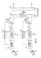
- Figure 1 is a block diagram of an optical transmission system in accordance with the present invention wherein an input signal travels over at least two parallel fiber links before being combined at the receiver end;
- Figure 2 is a block diagram of the receiving end in Figure 1 showing the delay control unit in more detail;
- Figure 3 is a block diagram of a novel pilot tone equalization circuit corresponding to the delay control unit of Figure 2.
- Figure 4 is a block diagram of an optical transmission system in accordance with the present invention where optic links are grouped into pairs each operating in a push-pull configuration.
- the present invention is concerned with improving the dynamic range of a single fiber optic link by dividing an RF input signal into a plurality of intermediate signals that are transmitted in parallel over respective fiber optic links before being individually detected and subsequently combined at a receiver end.
- the signal summation at the receiver end is accomplished with an RF power combiner, and provides an RF output signal having an enhanced signal to noise ratio in comparison to that of a single optical link.
- the present invention further includes a novel delay control circuit at the receiver end of each parallel link for equalizing the time-delay of the detected signal with the time-delay of the detected signals in the other parallel optic links.
- FIG. 1 is a block diagram of an optical transmission system constructed in accordance with the present invention, and shows two parallel links for exemplary purposes to illustrate the operation of the system.
- an RF input signal 9 enters a power splitter 10 and is divided equally between two intermediate signals 11 and 12.
- the intermediate signal 11 is coupled to a laser 13 which generates an optical signal representative of the electrical signal.
- the optical signal is then transmitted over an optical pathway means 14, such as fiber, and is detected by a photodiode 15 at the receiver end.
- the intermediate electrical signal 12 is converted to an optical signal by laser 13, coupled to an optical pathway means 14, and then detected by photodiode 15.
- the optical signals propagating along the optical pathway means arrive at the receiver end of their respective links at different times when the optical pathway means are fiber lines of unequal length.
- the output from each photodiode 15 is coupled to a delay control unit 16 which imposes the appropriate time delay on the detected signal. Further details of the delay control unit 16 will accompany the discussion hereinbelow of Figures 2 and 3.
- the time-delayed signals from the delay unit 16 in each parallel link are summed with an RF power combiner 17 and appear as a single RF output signal 18 having enhanced signal to noise ratio.
- the RF output signal 18 resulting from the summation of the in-phase detected signals exhibits a 3 dB increase in signal amplitude since the signal carried by each link is correlated.
- the uncorrelated noise sources do not increase in amplitude.
- This enhancement in signal to noise ratio is thus 3 dB better than that obtainable by a single link.
- resistive (lossy) summing is used after amplification of each individual photodetector output.
- any signal to noise ratio can be obtained using the appropriate number of parallel optic links.
- the detected signal output from each photodiode 15 is time-delayed by a delay control unit 16 before being coupled to combiner 17.
- the delay control unit 16 performs active delay equalization with a novel pilot tone phase detecting delay equalization circuit (hereinafter referred to as pilot tone equalization circuit) to allow operation at arbitrarily high frequency.
- the novel pilot tone equalization circuit is represented in Figure 2 as the closed-loop system consisting of electronic delay control 21, a pilot tone phase detector circuit 22, and a controller 23.
- pilot tone equalization circuit 16 initially requires that a pilot tone be added to the input signal 9 to produce a composite signal which is then coupled to splitter 10. Consequently, the spectrum of optical signal 20 which is coupled from optical pathway means 14 to photodiode 15 in each parallel link includes the information input signal 9 and the pilot tone.
- the detected signal is time-delayed by electronic delay control 21 and then coupled to pilot tone phase detector circuit 22, where the pilot tone is removed from the composite detected signal and phase detected to yield a control voltage proportional to the delay time of the respective parallel optic link.
- the controller 23 serves as a feedback mechanism in the closed-loop system for responding to the control voltage and continuously adjusting the electronic delay control 21 until the time delay is minimized.
- the pilot tone equalization circuit in each link operates in cooperation with the other circuits to equalize the delay times of the individual optical links as measured by the phase of the individually detected pilot tones.
- the controller 23 can be implemented as a normal continuous feedback control loop, or as a microprocessor which samples the individual phase detector outputs of each link.
- the electronic delay control 21 could be a motor driven line stretcher (trombone), electronically switched fixed length transmission lines, or other electronically or electro-mechanically controlled delay line.
- Figure 3 One possible implementation of the pilot tone equalization circuit according to the present invention is shown in Figure 3 where the elements designated by numerals 31, 32, 33, and 34 represent a single integrated unit corresponding functionally to the pilot tone phase detector circuit 22 in Figure 2.
- Figure 3 schematically illustrates how delay equalization is achieved between two pilot tone equalization circuits each coupled to a respective parallel link. To maintain consistency among the drawings, identically numbered items in Figures 2 and 3 represent the same component or subsystem.
- the optical signal 20 includes signals f s (input information signal) and f p (pilot tone).
- the pilot tone is removed from the detected signal with a filter network 31, amplified by amplifier 32, and then split into two intermediate tone signals by splitter 33.
- signal f s is routed to combiner 17 in Figure 1.
- Combiner 35 receives one intermediate pilot tone signal from each parallel link, and sums these signals to produce a phase reference signal present on combiner output 36.
- a phase locked loop (PLL) 37 can be used to remove noise from the phase reference if desired.
- the phase reference signal is distributed by splitter 38 to a phase detector 34 in each link where it serves as an input signal along with the other intermediate pilot tone from splitter 33.
- Phase detector 34 produces an output voltage proportional to the phase difference between the pilot tone of the respective link and the phase reference signal.
- the controller 23 responds to the phase detector voltage and adjusts the electronic delay control accordingly to minimize the phase detector output voltage. In this manner, delay variations between the various optical pathway means are equalized so that the information signal f s from each link is combined in-phase with the other information signals.
- the phase reference signal mentioned above is the average of the pilot tones from each link, the signal may also be an individual pilot tone from a selected one of the links.
- the two links in Figure 1 may be driven out of phase with respect to one another by using a 180° degree hybrid junction splitter 10 or suitable transformer (balun).
- the detected out-of-phase signals would then be brought back in-phase with a 180° degree combiner 17, or by performing signal inversion by reversing the polarity of one of the photodiodes 15 in the link pair and then using an in-phase power combiner 17.
- Another configuration would use an in-phase power splitter, a photodiode with reverse polarity relative to the other photodiode in the pair, and a 180° power combiner.
- the combined RF signal from each balanced pair is summed with the RF output signal from each other pair to produce a single output signal having both enhanced dynamic range and improved linearity.
Landscapes
- Physics & Mathematics (AREA)
- Electromagnetism (AREA)
- Engineering & Computer Science (AREA)
- Computer Networks & Wireless Communication (AREA)
- Signal Processing (AREA)
- Optical Communication System (AREA)
- Transmission Systems Not Characterized By The Medium Used For Transmission (AREA)
Abstract
Description
- The dynamic range of any analog fiber optic link is fundamentally limited by shot noise. For shot noise or quantum limited detection, it is well known that the signal to noise ratio, and hence the dynamic range, increases with the square root of the received optical power. For some applications, such as antenna-to-receiver Radio Frequency (RF) links, the dynamic range requirements are such that the required optical source power exceeds that available from a diode laser. Other noise sources present in practical optical links further degrade the signal to noise ratio.
- In one aspect of the present invention, an optical transmission system includes at a transmitter end a splitter means for dividing an RF input signal into a plurality of intermediate signals each assigned to a respective optical link. Each of the links includes a generator means for generating an optical signal representative of the respective RF intermediate signal, an optical pathway means for guiding the optical signal, and a detector means at the receiver end for performing optical detection. The detected signal from each optical link is coupled to a combiner means which provides an RF output signal having enhanced dynamic range.
- In another aspect of the present invention, each of the links includes a closed-loop delay equalization control circuit coupled to the detector means of said respective link for equalizing the time delay of the detected signal with that of the other detected signals. Operation of the control system requires a means for adding a pilot tone to the RF input signal. The closed-loop system includes a phase detector circuit responsive to the pilot tone for generating a control voltage proportional to the phase difference between the pilot tone and a common phase reference signal. A controller responds to the control voltage and adjusts an electronic delay control means to minimize the phase detector output voltage so that the delay variations between the detected signals are equalized.
In the drawings:
Figure 1 is a block diagram of an optical transmission system in accordance with the present invention wherein an input signal travels over at least two parallel fiber links before being combined at the receiver end;
Figure 2 is a block diagram of the receiving end in Figure 1 showing the delay control unit in more detail; and
Figure 3 is a block diagram of a novel pilot tone equalization circuit corresponding to the delay control unit of Figure 2.
Figure 4 is a block diagram of an optical transmission system in accordance with the present invention where optic links are grouped into pairs each operating in a push-pull configuration. - The present invention is concerned with improving the dynamic range of a single fiber optic link by dividing an RF input signal into a plurality of intermediate signals that are transmitted in parallel over respective fiber optic links before being individually detected and subsequently combined at a receiver end. The signal summation at the receiver end is accomplished with an RF power combiner, and provides an RF output signal having an enhanced signal to noise ratio in comparison to that of a single optical link. The present invention further includes a novel delay control circuit at the receiver end of each parallel link for equalizing the time-delay of the detected signal with the time-delay of the detected signals in the other parallel optic links.
- Figure 1 is a block diagram of an optical transmission system constructed in accordance with the present invention, and shows two parallel links for exemplary purposes to illustrate the operation of the system. As indicated, an
RF input signal 9 enters apower splitter 10 and is divided equally between twointermediate signals 11 and 12. The intermediate signal 11 is coupled to alaser 13 which generates an optical signal representative of the electrical signal. The optical signal is then transmitted over an optical pathway means 14, such as fiber, and is detected by aphotodiode 15 at the receiver end. Likewise, the intermediateelectrical signal 12 is converted to an optical signal bylaser 13, coupled to an optical pathway means 14, and then detected byphotodiode 15. Hereinafter, the interconnection oflaser 13, optical pathway means 14, andphotodiode 15 along a given signal path will be referred to as a parallel optic link, where the common numbering among the elements in each of the parallel links reflects the identical construction of the links. Although the discussion of Figure 1 concerns two parallel links, this should not serve as a limitation of the present invention since the system is clearly expandable to include a plurality of parallel optic links. - The optical signals propagating along the optical pathway means arrive at the receiver end of their respective links at different times when the optical pathway means are fiber lines of unequal length. In order to equalize the time delay among the detected signals, and thus bring the signals in-phase with one another before being combined, the output from each
photodiode 15 is coupled to adelay control unit 16 which imposes the appropriate time delay on the detected signal. Further details of thedelay control unit 16 will accompany the discussion hereinbelow of Figures 2 and 3. The time-delayed signals from thedelay unit 16 in each parallel link are summed with an RF power combiner 17 and appear as a singleRF output signal 18 having enhanced signal to noise ratio. - The
RF output signal 18 resulting from the summation of the in-phase detected signals exhibits a 3 dB increase in signal amplitude since the signal carried by each link is correlated. Advantageously, the uncorrelated noise sources do not increase in amplitude. This enhancement in signal to noise ratio is thus 3 dB better than that obtainable by a single link. A similar signal to noise enhancement occurs if resistive (lossy) summing is used after amplification of each individual photodetector output. As noted above, the present invention can be extended to include an arbitrary number of parallel optic links with suitable RF splitters and summers to provide a signal to noise enhancement over a single link. In general, this enhancement is quantitatively measured as
EF = 10 log n, where
EF = enhancement factor, and
n = number of parallel combined links. - Thus, any signal to noise ratio can be obtained using the appropriate number of parallel optic links.
- As mentioned above, the detected signal output from each
photodiode 15 is time-delayed by adelay control unit 16 before being coupled to combiner 17. The reason is that in order to achieve the enhancement in signal to noise ratio, all separate optical pathway means 14 must have delay times which are equal within a small fraction of the period (1/F) of the highest signal frequency (F) of interest. In accordance with another aspect of the invention, thedelay control unit 16 performs active delay equalization with a novel pilot tone phase detecting delay equalization circuit (hereinafter referred to as pilot tone equalization circuit) to allow operation at arbitrarily high frequency. The novel pilot tone equalization circuit is represented in Figure 2 as the closed-loop system consisting ofelectronic delay control 21, a pilot tonephase detector circuit 22, and acontroller 23. - Operation of the pilot
tone equalization circuit 16 initially requires that a pilot tone be added to theinput signal 9 to produce a composite signal which is then coupled to splitter 10. Consequently, the spectrum ofoptical signal 20 which is coupled from optical pathway means 14 tophotodiode 15 in each parallel link includes theinformation input signal 9 and the pilot tone. In a first pass through theequalization circuit 16, the detected signal is time-delayed byelectronic delay control 21 and then coupled to pilot tonephase detector circuit 22, where the pilot tone is removed from the composite detected signal and phase detected to yield a control voltage proportional to the delay time of the respective parallel optic link. - The
controller 23 serves as a feedback mechanism in the closed-loop system for responding to the control voltage and continuously adjusting theelectronic delay control 21 until the time delay is minimized. The pilot tone equalization circuit in each link operates in cooperation with the other circuits to equalize the delay times of the individual optical links as measured by the phase of the individually detected pilot tones. Thecontroller 23 can be implemented as a normal continuous feedback control loop, or as a microprocessor which samples the individual phase detector outputs of each link. Theelectronic delay control 21 could be a motor driven line stretcher (trombone), electronically switched fixed length transmission lines, or other electronically or electro-mechanically controlled delay line. - One possible implementation of the pilot tone equalization circuit according to the present invention is shown in Figure 3 where the elements designated by
numerals phase detector circuit 22 in Figure 2. Figure 3 schematically illustrates how delay equalization is achieved between two pilot tone equalization circuits each coupled to a respective parallel link. To maintain consistency among the drawings, identically numbered items in Figures 2 and 3 represent the same component or subsystem. - As shown, the
optical signal 20 includes signals fs (input information signal) and fp (pilot tone). Aftersignal 20 is detected byphotodiode 15, the pilot tone is removed from the detected signal with afilter network 31, amplified byamplifier 32, and then split into two intermediate tone signals bysplitter 33. Although not shown, signal fs is routed to combiner 17 in Figure 1.Combiner 35 receives one intermediate pilot tone signal from each parallel link, and sums these signals to produce a phase reference signal present on combineroutput 36. A phase locked loop (PLL) 37 can be used to remove noise from the phase reference if desired. The phase reference signal is distributed bysplitter 38 to aphase detector 34 in each link where it serves as an input signal along with the other intermediate pilot tone fromsplitter 33.Phase detector 34 produces an output voltage proportional to the phase difference between the pilot tone of the respective link and the phase reference signal. Thecontroller 23 responds to the phase detector voltage and adjusts the electronic delay control accordingly to minimize the phase detector output voltage. In this manner, delay variations between the various optical pathway means are equalized so that the information signal fs from each link is combined in-phase with the other information signals. Although the phase reference signal mentioned above is the average of the pilot tones from each link, the signal may also be an individual pilot tone from a selected one of the links. - In addition to the enhanced dynamic range, a significant reduction in even order distortion products is possible with the transmission system shown in Figure 4 by grouping the plurality of parallel optic links into exemplary link pairs 40 each including two parallel links 40(1) and 40(2), and operating each link pair in a push-pull configuration. The push-pull operation is characterized in that one of the links 40(1) in a pair is driven 180° out of phase with respect to the other link 40(2) in the pair. A mathematical model of a push-pull amplifier design is presented by W.H. Lambert in "Second-Order Distortion in CATV Push-Pull Amplifiers", Proceedings of the IEEE, Vol. 58, No. 7, 1970. The following discussion proposes several configurations to implement the push-pull operation, and refers illustratively to Figure 4 where the two parallel links 40(1) and 40(2) serve as a
link pair 40 where the common numbering between Figure 4 and Figure 1 reflects a similarity of components/subsystems. - The two links in Figure 1 may be driven out of phase with respect to one another by using a 180° degree
hybrid junction splitter 10 or suitable transformer (balun). The detected out-of-phase signals would then be brought back in-phase with a 180°degree combiner 17, or by performing signal inversion by reversing the polarity of one of thephotodiodes 15 in the link pair and then using an in-phase power combiner 17. Another configuration would use an in-phase power splitter, a photodiode with reverse polarity relative to the other photodiode in the pair, and a 180° power combiner. In each of the alternate configurations above, the combined RF signal from each balanced pair is summed with the RF output signal from each other pair to produce a single output signal having both enhanced dynamic range and improved linearity.
Claims (14)
- An optical transmission system for improving signal to noise ratio, comprising:
summation means for additively combining a pilot tone with an electrical input information signal to produce a composite electrical signal;
splitter means adapted to receive said composite signal and divide said composite signal into a plurality of equivalent intermediate signal each coupled to a respective one of a plurality of optical links;
each one of said optical links including:
generator means adapted to receive said respective intermediate signal and generate and optical signal representative of said respective intermediate signal,
optical pathway means coupled to the generator means of said one optical link for guiding said respective optical signal wherein said optical pathway means has an associated signal propagation delay time,
detector means adapted to receive the guided optical signal from the optical pathway means of said respective optical link and generate a detected electrical signal representative of said guided optical signal wherein said respective detected signal has an associated phase shift component proportional to the propagation delay time of said respective optical pathway means, and
a delay equalization circuit adapted to receive the detected signal from the detector means of said one optical link and equalize the phase shift component of said detected signal with the phase shift component of each detected signal in each remaining optical link of said plurality of optical links; and
means adapted to receive the equalized detected signal from the respective delay equalization circuit of each optical link and combine said equalized detected signals into a single output signal. - The optical transmission system as recited in claim 1 further including in each of said delay equalization circuits:
a closed-loop control system comprising:
an electronic delay control means having a signal input for receiving the detected signal from said respective detector means, a control input for controlling a time delay of said detected signal, and an output for providing a time-delayed version of said detected signal;
a filter network coupled to said delay control means for receiving the time-delayed detected signal and filtering out the pilot tone from the detected signal;
a phase detector responsive to a phase reference signal and the pilot tone from said filter network for producing an output voltage proportional to the phase difference between said pilot tone and said phase reference; and
a feedback controller responsive to said phase detector output voltage for providing a control signal to the control input of said electronic delay control means for continuously adjusting the time delay of said detected signal until the phase difference between said pilot tone and said phase reference reaches a desired value. - The optical transmission system as recited in claim 2 further including:
in each of said delay equalization circuits, splitter means coupled to said respective filter network for splitting said pilot tone into two intermediate pilot tones; and
a combiner for receiving one of said intermediate pilot tones from the respective filter network of each of said delay equalization circuits and providing said phase reference signal as the summation of said one intermediate tones. - The optical transmission system as recited in claim 2 wherein: said phase reference signal is the pilot tone from the respective filter network of a selected one of said links.
- An optical transmission system for improving signal to noise ratio, comprising:
summation means for additively combining a pilot tone with an electrical input information signal to produce a composite electrical signal;
input splitter means adapted to receive said composite signal and divide said composite signal into a plurality of equivalent intermediate composite signals;
a plurality of signal splitter means each adapted to receive a respective one of said equivalent intermediate composite signals and split said one intermediate composite signal into an associated first and second signal;
a plurality of optical link pairs each including an associated first and second optical link branch wherein the first branch has an output end and an input end to which is coupled a respective one of said first signals, while the associated second branch has an output end and an input end to which is coupled the second optical signal associated with said respective one first signal;
each optical link pair operating in a push-pull manner to drive the first signal of said respective first branch 180° out of phase with respect to the second signal of said associated second branch;
each of said first and second associated optical link branches in a respective optical link pair including:
generator means adapted to receive the signal associated with said branch and generate an optical signal representative of said signal,
optical pathway means coupled to said genrator means for guiding said generated optical signal wherein said optical pathway means has an associated signal propagation delay time,
detector means adapted to receive said guided optical signal and generate a detected electrical signal representative of said guided optical signal wherein said detected signal has an associated phase shift component proportional to the propagation delay time of said respective optical pathway means, and
a delay equalization circuit coupled to said detector means for equalizing the phase shift component of said detected signal with the phase shift component of each detected signal in each remaining optical link branch of said plurality of optical link branches;
in each of said optical link pairs, a combiner means adapted to receive the respective optical link pair and combine said equalized detected signals to produce a link pair output signal;
an output combiner means adapted to receive the link pair output signal from the respective combiner means of each optical link pair and combine said link pair output signals into an output signal of said optical transmission system. - The optical transmission system as recited in claim 5 wherein:
each of said signal splitter means includes a 180° power splitter; and
each of said combiner means includes a 180° power combiner. - The optical transmission system as recited in claim 5 wherein:
each of said signal splitter means includes a 180° splitter;
the detector means in each optical link branch includes a photodiode wherein for each first and second associated opitcal link branches in a respective optical link pair, the photodiode of said first branch has a reverse polarity with respect to the photodiode of said associated second branch; and
each of said combiner means includes a 0° power combiner. - The optical transmission system as recited in claim 5 wherein:
each of said signal splitter means includes a 0° power splitter;
the detector means in each optical link branch includes a photodiode wherein for each first and second associated optical link branches in a respective optical link pair, the photodiode of said first branch has a reverse polarity with respect to the photodiode of said associated second branch; and
each of said combiner means includes a 180° power combiner. - The optical transmission system as recited in claim 5 further further including in each delay equalization circuit:
an electronic delay control means having a signal input for receiving the detected signal from said respective detector means, a control input for controlling a time delay of said detected signal, and an output for providing a time-delayed version of said detected signal;
a filter network coupled to said delay control means for receiving the time-delayed detected signal and filtering out the pilot tone from the detected signal;
a phase detector responsive to a phase reference signal and the pilot tone from said associated filter network for producing an output voltage proportional to the phase difference between said pilot tone and said phase reference; and
a feedback controller responsive to said phase detector output voltage for providing a control signal to the control input of said electronic delay control means for continuously adjusting the time delay of said detected signal until the phase difference between said pilot tone and said phase reference reaches a desired value. - The optical transmission system as recited in claim 9 further including:
in each of said delay equalization circuits, a tone splitter means coupled to said respective filter network for splitting said pilot tone into two intermediate pilot tones; and
a combiner for receiving one of said intermediate pilot tones from the respective tone splitter means of each of said delay equalization circuits and combining said intermediate pilot tones to produce said phase reference signal. - The optical transmission system as recited in claim 9 wherein:
said reference signal is the pilot tone from the respective filter network of a selected one of said delay equalization circuits. - A system of closed-loop control circuits each coupled to a receiver end of a respective one of a plurality of parallel optical paths wherein each path provides a composite signal including an information siganl and pilot tone, each of said control circuits comprising:
an electronic delay control means having a signal input for receiving the composite signal from said respective path, a control input for controlling a time delay of said composite signal, and an output for providing a time-delayed version of said composite signal;
a filter network coupled to said delay control means for receiving the time-delayed composite signal and filtering out the pilot tone from the composite signal;
a phase detector responsive to a phase reference signal and the pilot tone from said filter network for producing an output voltage proportional to the phase difference between said pilot tone and said phase reference; and
a feedback controller responsive to said phase detector output voltage for providing a control signal to the control input of said electronic delay control means for continuously adjusting the time delay of said composite signal until the phase difference between said pilot tone and said phase reference reaches a desired value. - The system of control circuits as recited in claim 12 further including:
in each of said control circuits, splitter means coupled to said respective filter network for splitting said pilot tone into two intermediate pilot tones; and
a combiner for receiving one of said intermediate pilot tones from each of said control circuits and combining said intermediate pilot tones to produce said phase reference signal. - The optical transmission system as recited in claim 12 wherein:
said reference signal is the pilot tone from a selected one of said links.
Applications Claiming Priority (2)
| Application Number | Priority Date | Filing Date | Title |
|---|---|---|---|
| US454679 | 1989-12-21 | ||
| US07/454,679 US5023945A (en) | 1989-12-21 | 1989-12-21 | Transmission system using parallel optic links to achieve enhanced dynamic range |
Publications (2)
| Publication Number | Publication Date |
|---|---|
| EP0434004A1 true EP0434004A1 (en) | 1991-06-26 |
| EP0434004B1 EP0434004B1 (en) | 1995-06-28 |
Family
ID=23805628
Family Applications (1)
| Application Number | Title | Priority Date | Filing Date |
|---|---|---|---|
| EP90124639A Expired - Lifetime EP0434004B1 (en) | 1989-12-21 | 1990-12-18 | Transmission system using parallel optic links to achieve enhanced dynamic range |
Country Status (5)
| Country | Link |
|---|---|
| US (1) | US5023945A (en) |
| EP (1) | EP0434004B1 (en) |
| JP (1) | JP3147307B2 (en) |
| CA (1) | CA2032440C (en) |
| DE (1) | DE69020519T2 (en) |
Cited By (3)
| Publication number | Priority date | Publication date | Assignee | Title |
|---|---|---|---|---|
| WO1995020845A1 (en) * | 1994-01-28 | 1995-08-03 | Lee Communications Limited | Infrared data transmission system |
| WO2002051042A2 (en) * | 2000-12-19 | 2002-06-27 | Scientific-Atlanta, Inc. | Method and apparatus for suppressing relative intensity noise (rin) and improving transmission signals |
| EP1889383A1 (en) * | 2005-06-03 | 2008-02-20 | The Commonwealth Of Australia | Photonic link with improved dynamic range |
Families Citing this family (7)
| Publication number | Priority date | Publication date | Assignee | Title |
|---|---|---|---|---|
| AUPN957296A0 (en) | 1996-04-30 | 1996-05-23 | Cardiac Crc Nominees Pty Limited | A system for simultaneous unipolar multi-electrode ablation |
| US5940196A (en) * | 1997-05-16 | 1999-08-17 | Harmonic Lightwaves, Inc. | Optical communications system with wavelength division multiplexing |
| US7761011B2 (en) * | 2005-02-23 | 2010-07-20 | Kg Technology Associates, Inc. | Optical fiber communication link |
| US7766907B2 (en) * | 2006-12-28 | 2010-08-03 | St. Jude Medical, Atrial Fibrillation Division, Inc. | Ablation catheter with sensor array and discrimination circuit to minimize variation in power density |
| JP2010028751A (en) * | 2008-07-24 | 2010-02-04 | Toshiba Corp | Complementary optical wiring apparatus |
| JP2010136244A (en) * | 2008-12-08 | 2010-06-17 | Toshiba Corp | Transmission circuit and complementary optical wiring system |
| US11103308B2 (en) | 2017-12-11 | 2021-08-31 | Covidien Lp | Reusable transmission network for dividing energy and monitoring signals between surgical devices |
Citations (5)
| Publication number | Priority date | Publication date | Assignee | Title |
|---|---|---|---|---|
| US4128759A (en) * | 1977-11-21 | 1978-12-05 | The United States Of America As Represented By The Secretary Of The Navy | Fiber optic delay line filter |
| EP0010682A1 (en) * | 1978-10-27 | 1980-05-14 | Asea Ab | Device for transmitting analogue signals over an optical link |
| US4393518A (en) * | 1981-01-16 | 1983-07-12 | Bell Telephone Laboratories, Incorporated | Optical communication arrangement |
| FR2524229A1 (en) * | 1982-03-25 | 1983-09-30 | Anvar | Wideband low distortion transmission system for optical link - uses separate optical fibre to transmit electro=optic converter distortion signal |
| DE3844182A1 (en) * | 1988-12-29 | 1990-07-12 | Bosch Gmbh Robert | ANALOG OPTICAL TRANSMISSION SYSTEM |
Family Cites Families (7)
| Publication number | Priority date | Publication date | Assignee | Title |
|---|---|---|---|---|
| US3290504A (en) * | 1963-09-06 | 1966-12-06 | Itt | Distortion compensation of optoelectronic devices |
| US3666956A (en) * | 1966-02-03 | 1972-05-30 | Bbc Brown Boveri & Cie | Method and apparatus for telemetering by means utilizing modulated light beams |
| US4075474A (en) * | 1977-04-19 | 1978-02-21 | Northern Telecom Limited | Method and apparatus for distortion reduction in optical communication systems |
| DE2903327C2 (en) * | 1979-01-29 | 1983-04-07 | Siemens AG, 1000 Berlin und 8000 München | Circuit arrangement for the transmission of direct current signals between galvanically separated signal lines |
| NL7904431A (en) * | 1979-06-06 | 1980-12-09 | Philips Nv | OPTO-ELECTRONIC TRANSFER. |
| JPS57106247A (en) * | 1980-12-24 | 1982-07-02 | Hitachi Ltd | Analogue optical communication device |
| JPS59215136A (en) * | 1983-05-21 | 1984-12-05 | Nec Corp | Noise level supervising device of semiconductor laser |
-
1989
- 1989-12-21 US US07/454,679 patent/US5023945A/en not_active Expired - Lifetime
-
1990
- 1990-12-17 CA CA002032440A patent/CA2032440C/en not_active Expired - Lifetime
- 1990-12-18 DE DE69020519T patent/DE69020519T2/en not_active Expired - Lifetime
- 1990-12-18 EP EP90124639A patent/EP0434004B1/en not_active Expired - Lifetime
- 1990-12-21 JP JP41267190A patent/JP3147307B2/en not_active Expired - Lifetime
Patent Citations (5)
| Publication number | Priority date | Publication date | Assignee | Title |
|---|---|---|---|---|
| US4128759A (en) * | 1977-11-21 | 1978-12-05 | The United States Of America As Represented By The Secretary Of The Navy | Fiber optic delay line filter |
| EP0010682A1 (en) * | 1978-10-27 | 1980-05-14 | Asea Ab | Device for transmitting analogue signals over an optical link |
| US4393518A (en) * | 1981-01-16 | 1983-07-12 | Bell Telephone Laboratories, Incorporated | Optical communication arrangement |
| FR2524229A1 (en) * | 1982-03-25 | 1983-09-30 | Anvar | Wideband low distortion transmission system for optical link - uses separate optical fibre to transmit electro=optic converter distortion signal |
| DE3844182A1 (en) * | 1988-12-29 | 1990-07-12 | Bosch Gmbh Robert | ANALOG OPTICAL TRANSMISSION SYSTEM |
Cited By (6)
| Publication number | Priority date | Publication date | Assignee | Title |
|---|---|---|---|---|
| WO1995020845A1 (en) * | 1994-01-28 | 1995-08-03 | Lee Communications Limited | Infrared data transmission system |
| WO2002051042A2 (en) * | 2000-12-19 | 2002-06-27 | Scientific-Atlanta, Inc. | Method and apparatus for suppressing relative intensity noise (rin) and improving transmission signals |
| WO2002051042A3 (en) * | 2000-12-19 | 2002-08-29 | Scientific Atlanta | Method and apparatus for suppressing relative intensity noise (rin) and improving transmission signals |
| US6785474B2 (en) | 2000-12-19 | 2004-08-31 | Scientific-Atlanta, Inc. | Method and apparatus for suppressing relative intensity noise (RIN) and improving transmission signals |
| EP1889383A1 (en) * | 2005-06-03 | 2008-02-20 | The Commonwealth Of Australia | Photonic link with improved dynamic range |
| EP1889383A4 (en) * | 2005-06-03 | 2010-09-29 | Commw Of Australia | Photonic link with improved dynamic range |
Also Published As
| Publication number | Publication date |
|---|---|
| US5023945A (en) | 1991-06-11 |
| JPH04117035A (en) | 1992-04-17 |
| DE69020519T2 (en) | 1995-11-30 |
| DE69020519D1 (en) | 1995-08-03 |
| CA2032440C (en) | 2001-08-07 |
| EP0434004B1 (en) | 1995-06-28 |
| JP3147307B2 (en) | 2001-03-19 |
| CA2032440A1 (en) | 1991-06-22 |
Similar Documents
| Publication | Publication Date | Title |
|---|---|---|
| EP0543314B1 (en) | Optical signal equalizer for wavelength division multiplexed optical fiber systems | |
| US6606188B2 (en) | Optical repeater using raman amplification, wavelength division multiplexed light transmission system, excitation light supply method and excitation light control method for raman amplification | |
| EP0643320A2 (en) | Polarization-insensitive optical four-photon mixer | |
| JP2734969B2 (en) | Optical fiber amplifier for WDM transmission | |
| JP3983293B2 (en) | Improvements in or related to optical add / drop wavelength division multiplexing systems | |
| JPH08125634A (en) | Transmission system with optical amplifier | |
| US5023945A (en) | Transmission system using parallel optic links to achieve enhanced dynamic range | |
| JPH02134624A (en) | Polarization insensitive optical communication device using optical preamplification | |
| US5721637A (en) | Wavelength converter apparatus | |
| US4075474A (en) | Method and apparatus for distortion reduction in optical communication systems | |
| JPH0621897A (en) | Wavelength multiplex optical amplification relay transmission system and optical amplifier repeater | |
| US20030030895A1 (en) | Optical amplifiers and optical amplifying method for improved noise figure | |
| CN111819805A (en) | Variable equalizer and method of controlling the same | |
| US6169615B1 (en) | Wavelength division multiplex optical transmission apparatus | |
| US6097534A (en) | Optical amplifier system generating high optical output level | |
| JPH0378335A (en) | Stabilizing circuit for optical fsk frequency deviation | |
| US7120321B2 (en) | Control method and device for optical filter | |
| JP2774164B2 (en) | Optical amplifier | |
| JPH05235902A (en) | Receiver for optical wavelength division multiplex system | |
| USRE38359E1 (en) | Optical signal equalizer for wavelength division multiplexed optical fiber systems | |
| US20020080470A1 (en) | Optical amplifier and optically amplifying method | |
| JPH1022924A (en) | Optical amplifier device, and optical repeater amplifier device using the same | |
| JP2000106464A (en) | Direct optical amplifying device and method | |
| JP2765309B2 (en) | Optical selector | |
| JP2935298B2 (en) | Optical amplifier |
Legal Events
| Date | Code | Title | Description |
|---|---|---|---|
| PUAI | Public reference made under article 153(3) epc to a published international application that has entered the european phase |
Free format text: ORIGINAL CODE: 0009012 |
|
| AK | Designated contracting states |
Kind code of ref document: A1 Designated state(s): BE DE FR GB IT |
|
| 17P | Request for examination filed |
Effective date: 19911217 |
|
| 17Q | First examination report despatched |
Effective date: 19940121 |
|
| GRAA | (expected) grant |
Free format text: ORIGINAL CODE: 0009210 |
|
| AK | Designated contracting states |
Kind code of ref document: B1 Designated state(s): BE DE FR GB IT |
|
| ET | Fr: translation filed | ||
| REF | Corresponds to: |
Ref document number: 69020519 Country of ref document: DE Date of ref document: 19950803 |
|
| ITF | It: translation for a ep patent filed | ||
| PLBE | No opposition filed within time limit |
Free format text: ORIGINAL CODE: 0009261 |
|
| STAA | Information on the status of an ep patent application or granted ep patent |
Free format text: STATUS: NO OPPOSITION FILED WITHIN TIME LIMIT |
|
| 26N | No opposition filed | ||
| REG | Reference to a national code |
Ref country code: GB Ref legal event code: IF02 |
|
| PGFP | Annual fee paid to national office [announced via postgrant information from national office to epo] |
Ref country code: FR Payment date: 20031229 Year of fee payment: 14 |
|
| PG25 | Lapsed in a contracting state [announced via postgrant information from national office to epo] |
Ref country code: FR Free format text: LAPSE BECAUSE OF NON-PAYMENT OF DUE FEES Effective date: 20050831 |
|
| REG | Reference to a national code |
Ref country code: FR Ref legal event code: ST |
|
| PGFP | Annual fee paid to national office [announced via postgrant information from national office to epo] |
Ref country code: GB Payment date: 20091229 Year of fee payment: 20 |
|
| PGFP | Annual fee paid to national office [announced via postgrant information from national office to epo] |
Ref country code: IT Payment date: 20091230 Year of fee payment: 20 |
|
| PGFP | Annual fee paid to national office [announced via postgrant information from national office to epo] |
Ref country code: DE Payment date: 20091230 Year of fee payment: 20 Ref country code: BE Payment date: 20100212 Year of fee payment: 20 |
|
| BE20 | Be: patent expired |
Owner name: *VERIZON LABORATORIES INC. Effective date: 20101218 |
|
| REG | Reference to a national code |
Ref country code: GB Ref legal event code: PE20 Expiry date: 20101217 |
|
| PG25 | Lapsed in a contracting state [announced via postgrant information from national office to epo] |
Ref country code: GB Free format text: LAPSE BECAUSE OF EXPIRATION OF PROTECTION Effective date: 20101217 |
|
| PG25 | Lapsed in a contracting state [announced via postgrant information from national office to epo] |
Ref country code: DE Free format text: LAPSE BECAUSE OF EXPIRATION OF PROTECTION Effective date: 20101218 |