EP0433859B1 - Optical element and method for its production - Google Patents
Optical element and method for its production Download PDFInfo
- Publication number
- EP0433859B1 EP0433859B1 EP90123873A EP90123873A EP0433859B1 EP 0433859 B1 EP0433859 B1 EP 0433859B1 EP 90123873 A EP90123873 A EP 90123873A EP 90123873 A EP90123873 A EP 90123873A EP 0433859 B1 EP0433859 B1 EP 0433859B1
- Authority
- EP
- European Patent Office
- Prior art keywords
- ions
- substrate
- waveguide
- process according
- doped
- Prior art date
- Legal status (The legal status is an assumption and is not a legal conclusion. Google has not performed a legal analysis and makes no representation as to the accuracy of the status listed.)
- Expired - Lifetime
Links
Images

Classifications
-
- G—PHYSICS
- G02—OPTICS
- G02B—OPTICAL ELEMENTS, SYSTEMS OR APPARATUS
- G02B6/00—Light guides; Structural details of arrangements comprising light guides and other optical elements, e.g. couplings
- G02B6/10—Light guides; Structural details of arrangements comprising light guides and other optical elements, e.g. couplings of the optical waveguide type
- G02B6/12—Light guides; Structural details of arrangements comprising light guides and other optical elements, e.g. couplings of the optical waveguide type of the integrated circuit kind
- G02B6/13—Integrated optical circuits characterised by the manufacturing method
- G02B6/134—Integrated optical circuits characterised by the manufacturing method by substitution by dopant atoms
- G02B6/1347—Integrated optical circuits characterised by the manufacturing method by substitution by dopant atoms using ion implantation
Definitions
- the invention relates to a method for producing an optical component, in which a spatially restricted area of a substrate made of dielectric material, which is provided as an optical waveguide, is additionally doped with ions by implantation.
- the invention further relates to an optical component produced by such a method.
- Waveguides are described in the literature and are generally produced by the diffusion of metal ions or by ion exchange. Channels are defined by lithographic masks, similar to how conductor tracks or local dopings are made in microelectronics.
- the purpose of a waveguide is to guide light from one component to another without losses and without radiation, or to influence its bundled intensity, for example to modulate or attenuate it.
- ions If light interacts with certain atoms (ions), these ions can increase the intensity of the light through induced emission (light amplifier). This effect is particularly pronounced if the amplification takes place in a resonator delimited by reflectors.
- the laser is based on this principle.
- the energy required for amplification is either supplied optically (optical pumping) or can also be made available electrically in the case of semiconductor lasers.
- the known methods for producing an additional waveguide are therefore limited to light doping ions such as He and protons.
- the ions responsible for the light emission are introduced into an optical waveguide, one can specifically increase the intensity or construct a laser in the waveguide.
- rare earth ions e.g. Nd: YAG
- transition metal ions e.g. Ti: Al2O3
- their use is limited to the fact that the dielectric crystals or glasses are doped in the melt and thus the entire crystal or glass is more or less uniformly doped.
- Rare earth ions or ions of a transition metal are introduced as doping ions into the region of the waveguide by implantation with energies of 50 keV - 10 MeV.
- the ions are implanted in the waveguide region with an ion accelerator, the laser ions being able to be introduced in sufficient concentration to a sufficient depth below the surface.
- using the diffusion of the ions alone cannot achieve this.
- the doping can be limited laterally with the aid of lithographically structured masks.
- the doping is limited in depth by the implantation process itself.
- the ion implantation is carried out at substrate temperatures in the range from 300 K to 800 K, part of the lattice damage heals again during the implantation.
- substrate temperatures in the range from 300 K to 800 K
- part of the lattice damage heals again during the implantation.
- diffusion into the depth of the substrate does not take place, so that the depth of the doping is determined directly by the implantation energy.
- An alternative procedure is for the ion implantation to be carried out at substrate temperatures in the range from 77 K to 300 K. In this case, the lattice damage does not heal during the implantation. According to this alternative procedure in particular, subsequent heating of the substrate at temperatures from 800 K to 1800 K leads to a significant diffusion of the doping ions taking place during the heat treatment.
- the lattice damage remaining after the implantation can also be healed by solid-state epitaxy.
- Another variant of the method is that additional light ions, such as H, He or O, are implanted in the area of the substrate provided for the waveguide. As a result, lattice damage is generated at a greater depth and thus allows the doping ions to diffuse to a greater depth ("radiation damage - increased diffusion").
- additional light ions such as H, He or O
- a particularly advantageous procedure according to the invention is that spatially different regions of the substrate are doped with ions to produce spatially separate optical waveguides.
- the spatially different areas can also be doped in different concentrations or with different ions.
- the object according to the invention is thus achieved by a method according to claim 1, wherein rare-earth ions or ions of transition metals are implanted in the spatially restricted areas (the optical waveguides) as doping ions.
- a very advantageous embodiment of the component produced according to the invention consists in the fact that the substrate has regions (waveguides) which are spatially separated from one another and contain doping ions.
- the embodiment allows the construction of integrated optical solid-state lasers or light amplifiers.
- the spatially separated areas can also contain different doping ions or ions in different concentrations.
- FIG. 1 shows a homogeneously doped substrate DS (laser rod) of a known type.
- This component consists, for example, of a YAG crystal which is doped with Nd ions. Such components are doped in the melt.
- the laser rod according to FIG. 2 is a component as described in the literature cited.
- the substrate DS is doped homogeneously and a waveguide WL is additionally applied to a surface.
- the substrate DS can be the same material as in FIG. 1.
- the region L1 of the strip waveguide SWL doped with laser-active ions is a laser with two grating mirrors, and the region L2 likewise doped with laser-active ions is a laser with a grating mirror and an end surface mirror.
- the doped region V of the optical waveguide SWL is an optical amplifier. Pump light is fed in at the pump light inputs ⁇ p1, ⁇ p2 and ⁇ p3. ⁇ 1 is a light signal input.
- M1 and M2 are electro-optical modulators. A is the common output of all signals.
- the laser or amplifier regions V, L1 and L2 are doped with laser-active ions with the aid of ion implantation.
Landscapes
- Physics & Mathematics (AREA)
- Engineering & Computer Science (AREA)
- Microelectronics & Electronic Packaging (AREA)
- General Physics & Mathematics (AREA)
- Optics & Photonics (AREA)
- Optical Integrated Circuits (AREA)
- Lasers (AREA)
Description
Die Erfindung bezieht sich auf ein Verfahren zur Herstellung eines optischen Bauelementes, bei dem ein räumlich beschränkter, als optischer Wellenleiter vorgesehener Bereich eines Substrats aus dielektrischem Material zusätzlich mit Ionen durch Implantation dotiert wird. Die Erfindung bezieht sich ferner auf ein optisches Bauelement hergestellt nach einem solchen Verfahren.The invention relates to a method for producing an optical component, in which a spatially restricted area of a substrate made of dielectric material, which is provided as an optical waveguide, is additionally doped with ions by implantation. The invention further relates to an optical component produced by such a method.
Man kann Licht in optischen Materialien (Kristalle, Gläser) gebündelt transportieren. Der Kanal für Licht heißt optischer Wellenleiter. Wellenleiter sind in der Literatur beschrieben und werden im allgemeinen durch Eindiffusion von Metallionen oder durch Ionenaustausch hergestellt. Kanäle werden dabei durch lithographische Masken definiert, ähnlich wie in der Mikroelektronik Leiterbahnen oder lokale Dotierungen hergestellt werden. Sinn eines Wellenleiters ist es, Licht möglichst ohne Verluste und ohne Abstrahlung von einem Bauteil zu einem anderen zu führen oder es in seiner gebündelten Intensität zu beeinflussen, z.B. zu modulieren oder abzuschwächen.You can transport light bundled in optical materials (crystals, glasses). The channel for light is called optical waveguide. Waveguides are described in the literature and are generally produced by the diffusion of metal ions or by ion exchange. Channels are defined by lithographic masks, similar to how conductor tracks or local dopings are made in microelectronics. The purpose of a waveguide is to guide light from one component to another without losses and without radiation, or to influence its bundled intensity, for example to modulate or attenuate it.
Wenn Licht mit bestimmten Atomen (Ionen) wechselwirkt, können diese Ionen die Intensität des Lichtes durch induzierte Emission verstärken (Licht-Verstärker). Besonders ausgeprägt ist dieser Effekt, wenn die Verstärkung in einem durch Reflektoren begrenzten Resonator stattfindet. Auf diesem Prinzip beruht der Laser. Die zur Verstärkung notwendige Energie wird entweder optisch zugeführt (optisches Pumpen) oder kann bei Halbleiterlasern auch elektrisch zur Verfügung gestellt werden.If light interacts with certain atoms (ions), these ions can increase the intensity of the light through induced emission (light amplifier). This effect is particularly pronounced if the amplification takes place in a resonator delimited by reflectors. The laser is based on this principle. The energy required for amplification is either supplied optically (optical pumping) or can also be made available electrically in the case of semiconductor lasers.
Ein derartiges Verfahren ist aus Electronics-Letters 25, p. 985-986 (Juli 1989) bekannt. Danach wird einem gleichförmig dotierten Nd: YAG-Kristall mit Hilfe von He-Implantation ein zusätzlicher Wellenleiter aufgeprägt, der einen Lasereffekt zeigt.Such a method is known from Electronics Letters 25, p. 985-986 (July 1989). Then an additional waveguide is impressed on a uniformly doped Nd: YAG crystal with the aid of He implantation, which shows a laser effect.
Einer Arbeit von Lallier, Pocholle, Papuchon, Grezes-Besset, Pelletier, de Micheli, Li, He und Ostrowsky (Konferenzbeitrag bei der IOOC, Integr. Optics and Optical Communicatin, Kobe, Japan, July 1989) ist ferner zu entnehmen, daß einem Nd:MgO:LiNbO₃-Kristall mit Hilfe des Protonenaustausches ein Wellenleiter aufgeprägt wurde. Auch in diesem Falle wurde ein Lasereffekt beobachtet.A work by Lallier, Pocholle, Papuchon, Grezes-Besset, Pelletier, de Micheli, Li, He and Ostrowsky (conference contribution to IOOC, Integr. Optics and Optical Communicatin, Kobe, Japan, July 1989) also shows that one Nd: MgO: LiNbO₃ crystal with the help of proton exchange a waveguide was impressed. A laser effect was also observed in this case.
Die bekannten Verfahren zur Erzeugung eines zusätzlichen Wellenleiters beschränken sich somit auf leichte Dotierungs-Ionen wie He und Protonen.The known methods for producing an additional waveguide are therefore limited to light doping ions such as He and protons.
Wenn man die für die Licht-Emission verantwortlichen Ionen in einen optischen Wellenleiter einbringt, kann man gezielt Intensität verstärken oder einen Laser im Wellenleiter konstruieren.If the ions responsible for the light emission are introduced into an optical waveguide, one can specifically increase the intensity or construct a laser in the waveguide.
Die Benutzung von Seltenen-Erd-Ionen (z.B. Nd:YAG) oder Übergangsmetall-Ionen (z.B. Ti:Al₂O₃) als Dotierungs-Ionen zur Herstellung von Festkörperlasern ist bekannt. Ihr Einsatz beschränkt sich jedoch darauf, daß die dielektrischen Kristalle oder Gläser in der Schmelze dotiert werden und somit der gesamte Kristall bzw. das Glas mehr oder minder gleichmäßig dotiert ist.The use of rare earth ions (e.g. Nd: YAG) or transition metal ions (e.g. Ti: Al₂O₃) as doping ions for the production of solid-state lasers is known. However, their use is limited to the fact that the dielectric crystals or glasses are doped in the melt and thus the entire crystal or glass is more or less uniformly doped.
Bei derart gleichmäßig dotierten "Laserkristallen" ist es außerordentlich ungünstig, daß auf diesem dotierten Substrat weitere Bauelemente der Wellenleiteroptik wie etwa Modulatoren, Lichtkoppler und Strahlweichen nicht optimal untergebracht werden können, weil in diesen Bauteilen die Laserionen unerwünscht Absorption oder Streuung hervorrufen können. Außerdem sind unterschiedlich dotierte Strukturen nicht möglich.With such uniformly doped "laser crystals", it is extremely unfavorable that other components of the waveguide optics such as modulators, light couplers and beam switches cannot be optimally accommodated on this doped substrate, because in these components the laser ions can cause unwanted absorption or scattering. In addition, differently doped structures are not possible.
Aus einer Reihe von Gründen wäre es vorteilhaft, wenn nicht ein großes Kristallstück für die Verstärker-und Laserwirkung eingesetzt wird, sondern das Licht auf einen optischen Wellenleiter begrenzt wird, der in den seitlichen Dimensionen vergleichbar ist mit der Ausdehnung des anzukoppelnden Lichtleiters, so daß das Licht leichter in eine Lichtfaser eingekoppelt werden kann. Als Vorteile eines solchen Bauelementes sind zu nennen:
- 1. Wesentliche Reduzierung der optischen Pumpleistung
- 2. Leichtere Beeinflußbarkeit der Felder in der Cavity für Mode-Locking oder Q-Switching
- 3. Ausnutzung von nichtlinearen Eigenschaften für Second-Harmonic-Generation Differenzfrequenzbildung oder Summenfrequenzbildung
- 4. Günstige Voraussetzungen für die Ankopplung eines optischen Lichtleiters
- 1. Significant reduction in optical pumping power
- 2. Easier influenceability of the fields in the cavity for mode locking or Q switching
- 3. Exploitation of non-linear properties for second harmonic generation difference frequency formation or sum frequency formation
- 4. Favorable conditions for coupling an optical light guide
Es ist daher Aufgabe der Erfindung, ein Verfahren zur Herstellung eines Bauelementes der eingangs bezeichneten Art zu schaffen, das es ermöglicht, einen zusätzlichen, als optischen Wellenleiter fungierenden Bereich des Substrats mit Laserionen zu dotieren. Es ist ferner Aufgabe der Erfindung, ein Bauelement zu schaffen, das den Lasereffekt ermöglichende optische Wellenleiter aufweist und das im weiteren Ausbau die Integration mehrerer optischer Bauelemente zusammen mit einem oder mehreren Lasern auf einem gemeinsamen Substrat in optimaler Weise ermöglicht.It is therefore an object of the invention to provide a method for producing a component of the type described at the outset, which makes it possible to dope an additional region of the substrate which functions as an optical waveguide with laser ions. It is also an object of the invention to provide a component which has the optical waveguide which enables the laser effect and which, in the further expansion, enables the integration of a plurality of optical components together with one or more lasers on a common substrate in an optimal manner.
Diese Aufgabe wird erfindungsgemäß durch ein Verfahren nach Anspruch 1 gelöst. Hierbei werden als Dotierungs-Ionen Seltene-Erd-Ionen oder Ionen eines Übergangsmetalls durch Implantation mit Energien von 50 keV - 10 MeV in den Bereich des Wellenleiters eingebracht. Die Ionen werden dazu mit einem Ionenbeschleuniger in den Wellenleiterbereich implantiert, wobei die Laserionen in ausreichender Konzentration bis in eine hinreichende Tiefe unterhalb der Oberfläche eingebracht werden können. Durch Anwendung der Diffusion der Ionen allein kann dies dagegen nicht erreicht werden.This object is achieved by a method according to claim 1. Rare earth ions or ions of a transition metal are introduced as doping ions into the region of the waveguide by implantation with energies of 50 keV - 10 MeV. For this purpose, the ions are implanted in the waveguide region with an ion accelerator, the laser ions being able to be introduced in sufficient concentration to a sufficient depth below the surface. By contrast, using the diffusion of the ions alone cannot achieve this.
Mit Hilfe lithographisch strukturierter Masken läßt sich die Dotierung lateral begrenzen. Durch den Implantationsprozeß selbst ist die Dotierung in der Tiefe begrenzt.The doping can be limited laterally with the aid of lithographically structured masks. The doping is limited in depth by the implantation process itself.
Wird die Ionen-Implantation bei Substrattemperaturen im Bereich von 300 K bis 800 K durchgeführt, dann heilt schon während der Implantation ein Teil des Gitterschadens wieder aus. Im Falle von Seltenen-Erd-Ionen findet eine Diffusion in die Tiefe des Substrat nicht statt, so daß die Tiefe der Dotierung direkt durch die Implantationsenergie bestimmt ist.If the ion implantation is carried out at substrate temperatures in the range from 300 K to 800 K, part of the lattice damage heals again during the implantation. In the case of rare earth ions, diffusion into the depth of the substrate does not take place, so that the depth of the doping is determined directly by the implantation energy.
Eine alternative Verfahrensweise besteht darin, daß die Ionen-Implantation bei Substrat-Temperaturen im Bereich von 77 K bis 300 K durchgeführt werden. In diesem Falle heilt der Gitterschaden während der Implantation nicht aus. Insbesondere nach dieser alternativen Verfahrensweise führt eine nachträgliche Temperung des Substrats bei Temperaturen von 800 K bis 1800 K dazu, daß während der Wärmebehandlung eine deutliche Diffusion der Dotierungs-Ionen stattfindet.An alternative procedure is for the ion implantation to be carried out at substrate temperatures in the range from 77 K to 300 K. In this case, the lattice damage does not heal during the implantation. According to this alternative procedure in particular, subsequent heating of the substrate at temperatures from 800 K to 1800 K leads to a significant diffusion of the doping ions taking place during the heat treatment.
Der nach der Implantation verbleibende Gitterschaden kann auch durch Festkörperepitaxie ausgeheilt werden.The lattice damage remaining after the implantation can also be healed by solid-state epitaxy.
Eine weitere Verfahrensvariante besteht darin, daß zusätzliche leichte Ionen, wie H, He oder O, in den für den Wellenleiter vorgesehenen Bereich des Substrats implantiert werden. Hierdurch werden Gitterschäden in größerer Tiefe erzeugt und damit eine Diffusion der Dotierungs-Ionen in größere Tiefe ermöglicht ("Strahlenschaden - verstärkte Diffusion").Another variant of the method is that additional light ions, such as H, He or O, are implanted in the area of the substrate provided for the waveguide. As a result, lattice damage is generated at a greater depth and thus allows the doping ions to diffuse to a greater depth ("radiation damage - increased diffusion").
Eine besonders vorteilhafte Verfahrensweise gemäß der Erfindung besteht darin, daß räumlich unterschiedlichen Bereiche des Substrats zur Erzeugung räumlich voneinander getrennter optischer Wellenleiter mit Ionen dotiert werden. Die räumlich unterschiedlichen Bereiche können dabei auch in unterschiedlicher Konzentration oder mit unterschiedlichen Ionen dotiert werden. Dies bedeutet, daß in demselben, bevorzugt undotierten Mutterkristall (z.B.: ein LiNbO₃-Wafer oder ein optisches Glas) an verschiedenen Orten unterschiedliche Laserionendotierungen vorgenommen werden, so daß Laser oder Verstärker verschiedener Wellenlängen und unterschiedlicher Konstruktionen (Gitterspiegel, Gitterresonatoren, Oberflächenspiegel, gekoppelte Wellenleiter, intracavity modulierte Laser) auf demselben Chip integriert werden können, zusammen mit weiteren Bauelementen.A particularly advantageous procedure according to the invention is that spatially different regions of the substrate are doped with ions to produce spatially separate optical waveguides. The spatially different areas can also be doped in different concentrations or with different ions. This means that in the same, preferably undoped mother crystal (eg: a LiNbO₃ wafer or an optical glass) different laser ion doping is carried out at different locations, so that lasers or amplifiers of different wavelengths and different Constructions (grating mirrors, grating resonators, surface mirrors, coupled waveguides, intracavity modulated lasers) can be integrated on the same chip, together with other components.
Diese günstige Kombination verschiedenartiger Laser-Dotierungsionen, gegebenenfalls mit unterschiedlichen Konzentrationen, läßt sich nicht mit den sonst üblichen Diffusionsdotierungen erreichen, weil die für den Lasereffekt notwendigen Ionen, insbesondere die Seltene-Erd-Ionen, zu große Atomdurchmesser besitzen und sich häufig nicht durch Diffusion eintreiben lassen.This favorable combination of different types of laser doping ions, possibly with different concentrations, cannot be achieved with the usual diffusion doping, because the ions necessary for the laser effect, in particular the rare earth ions, have atomic diameters that are too large and often do not penetrate through diffusion to let.
Die Aufgabe gemäß der Erfindung wird somit durch ein Verfahren nach Anspruch 1 gelöst, wobei in die räumlich beschränkten Bereiche (die optischen Wellenleiter) als Dotierungs-Ionen Seltene-Erd-Ionen oder Ionen von Übergangsmetallen implantiert werden.The object according to the invention is thus achieved by a method according to claim 1, wherein rare-earth ions or ions of transition metals are implanted in the spatially restricted areas (the optical waveguides) as doping ions.
Eine sehr vorteilhafte Ausführungsform des Bauelementes hergestellt gemäß der Erfindung besteht dabei darin, daß das Substrat räumlich voneinander getrennte, Dotierungs-Ionen enthaltende Bereiche (Wellenleiter) aufweist. Die Ausführungsform erlaubt den Bau von integriert-optischen Festkörper-Lasern oder Lichtverstärkern. Dabei können die räumlich voneinander getrennten Bereiche auch unterschiedliche Dotierungs-Ionen bzw. Ionen in unterschiedlicher Konzentration enthalten.A very advantageous embodiment of the component produced according to the invention consists in the fact that the substrate has regions (waveguides) which are spatially separated from one another and contain doping ions. The embodiment allows the construction of integrated optical solid-state lasers or light amplifiers. The spatially separated areas can also contain different doping ions or ions in different concentrations.
Ausführungsformen der Bauelemente gemäß der Erfindung werden in der Zeichnung schematisch dargestellt und im folgenden näher erläutert:Embodiments of the components according to the invention are shown schematically in the drawing and explained in more detail below:
Es zeigen
- Figur 1
- einen homogen dotierten Laserstab bekannter Art
- Figur 2
- einen homogen dotierten Laserstab mit zusätzlichem Wellenleiter an einer Oberfläche
- Figur 3
- einen Streifenwellenleiter in einem optischen Kristall mit einer Laserdotierung nur im Bereich des Wellenleiters
- Figur 4
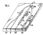
- ein integrierter optischer Verstärker und 2 Laser mit externen Modulatoren für 3 Frequenzen
- Figure 1
- a homogeneously doped laser rod of known type
- Figure 2
- a homogeneously doped laser rod with an additional waveguide on one surface
- Figure 3
- a strip waveguide in an optical crystal with laser doping only in the area of the waveguide
- Figure 4
- an integrated optical amplifier and 2 lasers with external modulators for 3 frequencies
In Figur 1 ist ein homogen dotiertes Substrat DS (Laserstab) bekannter Art dargestellt. Dieses Bauelement besteht beispielsweise aus einem YAG-Kristall, der mit Nd-Ionen dotiert ist. Derartige Bauelemente werden in der Schmelze dotiert.FIG. 1 shows a homogeneously doped substrate DS (laser rod) of a known type. This component consists, for example, of a YAG crystal which is doped with Nd ions. Such components are doped in the melt.
Beim Laserstab gemäß Figur 2 handelt es sich um ein Bauelement, wie in der zitierten Literatur beschrieben. Das Substrat DS ist homogen dotiert und zusätzlich ist ein Wellenleiter WL an einer Oberfläche aufgebracht. Bei dem Substrat DS kann es sich um dasselbe Material wie in Fig. 1 handeln.The laser rod according to FIG. 2 is a component as described in the literature cited. The substrate DS is doped homogeneously and a waveguide WL is additionally applied to a surface. The substrate DS can be the same material as in FIG. 1.
Bei dem in Figur 3 dargestellten Bauelement handelt es sich beispielsweise um einen LiNbO₃-Kristall (undodiertes Substrat US) mit einem mit Er-Ionen dotierten Streifenwellenleiter SWL. Ein solches Bauelement wird beispielsweise erfindungsgemäß wie folgt hergestellt:
- 1. In den LNbO₃-Kristall (Substrat) werden unter lateraler Begrenzung durch Ti-Masken (lithographisch; 1 »m Dicke) Er-Ionen mit 200 keV mit einer Dotierung von 10¹⁶ Er/cm² implantiert. Die Er-Ionen erreichen eine Tiefe von 70 - 80 nm. Die Ti-Maske wird mittels 5 %iger HF-Säure abgeätzt.
- 2. Die Probe wird bei 1050 C° in trockener Luft 13 Stunden getempert, wonach die Er-Ionen eine Tiefe von 1,5 - 2 »m erreichen.
- 3. Der Streifenwellenleiter wird in bekannter Weise durch
- a) Ti-Enddiffusion,
- b) Protonen-Austausch oder
- c) Ti-Implantation
- 1. In the LNbO₃ crystal (substrate) Er ions with 200 keV with a doping of 10¹⁶ Er / cm² are implanted under lateral delimitation by Ti masks (lithographic; 1 »m thickness). The Er ions reach a depth of 70-80 nm. The Ti mask is etched away with 5% HF acid.
- 2. The sample is annealed at 1050 ° C in dry air for 13 hours, after which the Er ions reach a depth of 1.5 - 2 »m.
- 3. The strip waveguide is passed through in a known manner
- a) final Ti diffusion,
- b) proton exchange or
- c) Ti implantation
Bei dem in Figur 4 dargestellten Bauelement befinden sich mehrere Streifenwellenleiter SWL auf einem undotierten Substrat US, beispielsweise einem Kristall aus LiNbO₃. Der mit laseraktiven Ionen dotierte Bereich L1 des Streifenwellenleiters SWL ist ein Laser mit zwei Gitterspiegeln, der ebenfalls mit laseraktiven Ionen dotierte Bereich L2 ist ein Laser mit einem Gitterspiegel und einem Endflächenspiegel. Der dotierte Bereich V des optischen Wellenleiters SWL ist ein optischer Verstärker. Pumplicht wird bei den Pumplichteingängen λp1, λp2 und λp3 eingespeist. λ1 ist ein Lichtsignaleingang. M1 und M2 sind elektro-optische Modulatoren. A ist der gemeinsame Ausgang aller Signale. In diesem integriert-optischen Chip sind zusätzlich zu den bekannten Verfahren der Herstellung von integriert-optischen Bauelementen die Laser- oder Verstärkerbereiche V, L1 und L2 mit Hilfe der Ionenimplantation mit laseraktiven Ionen dotiert.In the component shown in Figure 4, there are a plurality of strip waveguides SWL on an undoped substrate US, for example a crystal made of LiNbO₃. The region L1 of the strip waveguide SWL doped with laser-active ions is a laser with two grating mirrors, and the region L2 likewise doped with laser-active ions is a laser with a grating mirror and an end surface mirror. The doped region V of the optical waveguide SWL is an optical amplifier. Pump light is fed in at the pump light inputs λp1, λp2 and λp3. λ1 is a light signal input. M1 and M2 are electro-optical modulators. A is the common output of all signals. In this integrated-optical chip, in addition to the known methods of producing integrated-optical components, the laser or amplifier regions V, L1 and L2 are doped with laser-active ions with the aid of ion implantation.
Claims (9)
- Process for the production of a waveguide-amplifier which in a spatially restricted region of an optical waveguide in a substrate made of dielectric material has as doping ions rare-earth ions or ions of a transition metal for the amplification of light conducted in the waveguide, characterised in that the doping ions are introduced by implantation with energies of 50 keV - 10 MeV.
- Process according to claim 1, characterised in that the substrate is an LiNbO₃ crystal.
- Process according to claim 1 or 2, characterised in that masks are used for the doping of the spatially restricted region of the optical waveguide (SWL).
- Process according to claim 1, 2 or 3, characterised in that the ion implantation is carried out at substrate temperatures in the region of 300 K to 800 K.
- Process according to one of claims 1, 2 or 3, characterised in that the ion implantation is carried out at substrate temperatures in the region of 77 K to 300 K.
- Process according to claim 5, characterised in that the lattice damage caused by the ion implantation in the substrate (US) is healed by tempering of the substrate at a temperature of 800 K to 1800 K.
- Process according to one of the preceding claims, characterised in that ions of a light type such as H, He or O are additionally implanted in the spatially restricted region of the waveguide.
- Process according to one of the preceding claims, characterised in that differing spatially restricted regions of the substrate (US) are doped with ions for the production of waveguide-amplifiers (V, L1, L2) which are spatially separate from one another.
- Process according to claim 8, characterised in that the differing spatially restricted regions are doped with differing ions.
Applications Claiming Priority (4)
| Application Number | Priority Date | Filing Date | Title |
|---|---|---|---|
| DE3941704 | 1989-12-18 | ||
| DE3941704 | 1989-12-18 | ||
| DE4022090A DE4022090A1 (en) | 1989-12-18 | 1990-07-11 | ELECTRO-OPTICAL COMPONENT AND METHOD FOR THE PRODUCTION THEREOF |
| DE4022090 | 1990-07-11 |
Publications (2)
| Publication Number | Publication Date |
|---|---|
| EP0433859A1 EP0433859A1 (en) | 1991-06-26 |
| EP0433859B1 true EP0433859B1 (en) | 1994-09-28 |
Family
ID=25888098
Family Applications (1)
| Application Number | Title | Priority Date | Filing Date |
|---|---|---|---|
| EP90123873A Expired - Lifetime EP0433859B1 (en) | 1989-12-18 | 1990-12-12 | Optical element and method for its production |
Country Status (4)
| Country | Link |
|---|---|
| US (2) | US5174876A (en) |
| EP (1) | EP0433859B1 (en) |
| JP (1) | JPH03200125A (en) |
| DE (2) | DE4022090A1 (en) |
Families Citing this family (57)
| Publication number | Priority date | Publication date | Assignee | Title |
|---|---|---|---|---|
| DE4022090A1 (en) * | 1989-12-18 | 1991-06-20 | Forschungszentrum Juelich Gmbh | ELECTRO-OPTICAL COMPONENT AND METHOD FOR THE PRODUCTION THEREOF |
| DE4113354A1 (en) * | 1991-04-24 | 1992-10-29 | Siemens Ag | OPTICALLY PUMPED WAVE GUIDE |
| US5227913A (en) * | 1991-09-11 | 1993-07-13 | Wisconsin Alumni Research Foundation | Co-deposition of erbium and titanium into lithium niobate and optical amplifier produced thereby |
| DE4136511C2 (en) * | 1991-11-06 | 1995-06-08 | Forschungszentrum Juelich Gmbh | Process for the production of a Si / FeSi¶2¶ heterostructure |
| US5424244A (en) * | 1992-03-26 | 1995-06-13 | Semiconductor Energy Laboratory Co., Ltd. | Process for laser processing and apparatus for use in the same |
| US5250098A (en) * | 1992-07-27 | 1993-10-05 | Ford Motor Company | Thermally durable anti-reflective glass |
| US5343542A (en) * | 1993-04-22 | 1994-08-30 | International Business Machines Corporation | Tapered fabry-perot waveguide optical demultiplexer |
| US5394489A (en) * | 1993-07-27 | 1995-02-28 | At&T Corp. | Wavelength division multiplexed optical communication transmitters |
| DE4339401C1 (en) * | 1993-11-18 | 1994-12-22 | Forschungszentrum Juelich Gmbh | Process for producing a layer structure and its use |
| US5608826A (en) * | 1994-06-09 | 1997-03-04 | Apa Optics, Inc. | Wavelength division multiplexed optical modulator and multiplexing method using same |
| USH1848H (en) * | 1997-08-18 | 2000-05-02 | Amin; Jaymin | Z-propagating waveguide laser and amplifier device in rare-earth-doped LiNbO3 |
| US6441934B1 (en) | 1998-02-13 | 2002-08-27 | Apa Optics, Inc. | Multiplexer and demultiplexer for single mode optical fiber communication links |
| US6647209B1 (en) | 1998-02-13 | 2003-11-11 | Apa Optics, Inc. | Multiplexer and demultiplexer for single mode optical fiber communication links |
| US6434294B1 (en) | 1998-09-02 | 2002-08-13 | Bae Systems Aerospace Electronics Inc. | Photonic local oscillator signal generator and method for generating a local oscillator signal |
| US6330388B1 (en) * | 1999-01-27 | 2001-12-11 | Northstar Photonics, Inc. | Method and apparatus for waveguide optics and devices |
| US6538805B1 (en) | 1999-02-19 | 2003-03-25 | Photon-X, Inc. | Codopant polymers for efficient optical amplification |
| US6292292B1 (en) | 2000-02-18 | 2001-09-18 | Photon-X | Rare earth polymers, optical amplifiers and optical fibers |
| US20040201000A1 (en) * | 1999-02-19 | 2004-10-14 | Photon-X, Inc. | Polymer blends for optical amplification |
| US6734453B2 (en) | 2000-08-08 | 2004-05-11 | Translucent Photonics, Inc. | Devices with optical gain in silicon |
| US7469558B2 (en) | 2001-07-10 | 2008-12-30 | Springworks, Llc | As-deposited planar optical waveguides with low scattering loss and methods for their manufacture |
| US7404877B2 (en) | 2001-11-09 | 2008-07-29 | Springworks, Llc | Low temperature zirconia based thermal barrier layer by PVD |
| AU2003221350A1 (en) * | 2002-03-13 | 2003-09-22 | Nikon Corporation | Light amplifying device and method of manufacturing the device, light source device using the light amplifying device, light treatment device using the light source device, and exposure device using the light source device |
| US6884327B2 (en) | 2002-03-16 | 2005-04-26 | Tao Pan | Mode size converter for a planar waveguide |
| US7378356B2 (en) | 2002-03-16 | 2008-05-27 | Springworks, Llc | Biased pulse DC reactive sputtering of oxide films |
| US20030194162A1 (en) * | 2002-03-26 | 2003-10-16 | Mininni Robert M. | Fluorinated and halogenated phosphinic acids and their active metal derivatives |
| US8431264B2 (en) | 2002-08-09 | 2013-04-30 | Infinite Power Solutions, Inc. | Hybrid thin-film battery |
| US8021778B2 (en) | 2002-08-09 | 2011-09-20 | Infinite Power Solutions, Inc. | Electrochemical apparatus with barrier layer protected substrate |
| US8445130B2 (en) | 2002-08-09 | 2013-05-21 | Infinite Power Solutions, Inc. | Hybrid thin-film battery |
| US7993773B2 (en) | 2002-08-09 | 2011-08-09 | Infinite Power Solutions, Inc. | Electrochemical apparatus with barrier layer protected substrate |
| US8394522B2 (en) | 2002-08-09 | 2013-03-12 | Infinite Power Solutions, Inc. | Robust metal film encapsulation |
| US8404376B2 (en) | 2002-08-09 | 2013-03-26 | Infinite Power Solutions, Inc. | Metal film encapsulation |
| US8236443B2 (en) | 2002-08-09 | 2012-08-07 | Infinite Power Solutions, Inc. | Metal film encapsulation |
| US20070264564A1 (en) | 2006-03-16 | 2007-11-15 | Infinite Power Solutions, Inc. | Thin film battery on an integrated circuit or circuit board and method thereof |
| AU2003261463A1 (en) | 2002-08-27 | 2004-03-19 | Symmorphix, Inc. | Optically coupling into highly uniform waveguides |
| CN1756856B (en) | 2003-02-27 | 2011-10-12 | 希莫菲克斯公司 | Dielectric barrier layer films |
| US7238628B2 (en) | 2003-05-23 | 2007-07-03 | Symmorphix, Inc. | Energy conversion and storage films and devices by physical vapor deposition of titanium and titanium oxides and sub-oxides |
| US8728285B2 (en) | 2003-05-23 | 2014-05-20 | Demaray, Llc | Transparent conductive oxides |
| ITCZ20040017A1 (en) * | 2004-11-08 | 2005-02-08 | Carlo Gavazzi Space Spa | INTEGRATED MICRO-INTERFEROMETER AND METHOD OF REALIZATION |
| US7959769B2 (en) | 2004-12-08 | 2011-06-14 | Infinite Power Solutions, Inc. | Deposition of LiCoO2 |
| US8636876B2 (en) | 2004-12-08 | 2014-01-28 | R. Ernest Demaray | Deposition of LiCoO2 |
| JP4359252B2 (en) * | 2005-03-14 | 2009-11-04 | 株式会社日立製作所 | Tunable semiconductor laser device |
| US7838133B2 (en) | 2005-09-02 | 2010-11-23 | Springworks, Llc | Deposition of perovskite and other compound ceramic films for dielectric applications |
| CN101523571A (en) | 2006-09-29 | 2009-09-02 | 无穷动力解决方案股份有限公司 | Masking and material confinement of a battery layer deposited on a flexible substrate |
| US8197781B2 (en) | 2006-11-07 | 2012-06-12 | Infinite Power Solutions, Inc. | Sputtering target of Li3PO4 and method for producing same |
| KR20150128817A (en) | 2007-12-21 | 2015-11-18 | 사푸라스트 리써치 엘엘씨 | Method for sputter targets for electrolyte films |
| US8268488B2 (en) | 2007-12-21 | 2012-09-18 | Infinite Power Solutions, Inc. | Thin film electrolyte for thin film batteries |
| WO2009089417A1 (en) | 2008-01-11 | 2009-07-16 | Infinite Power Solutions, Inc. | Thin film encapsulation for thin film batteries and other devices |
| KR101672254B1 (en) | 2008-04-02 | 2016-11-08 | 사푸라스트 리써치 엘엘씨 | Passive over/under voltage control and protection for energy storage devices associated with energy harvesting |
| EP2319101B1 (en) | 2008-08-11 | 2015-11-04 | Sapurast Research LLC | Energy device with integral collector surface for electromagnetic energy harvesting and method thereof |
| EP2332127A4 (en) | 2008-09-12 | 2011-11-09 | Infinite Power Solutions Inc | Energy device with integral conductive surface for data communication via electromagnetic energy and method thereof |
| WO2010042594A1 (en) | 2008-10-08 | 2010-04-15 | Infinite Power Solutions, Inc. | Environmentally-powered wireless sensor module |
| KR101792287B1 (en) | 2009-09-01 | 2017-10-31 | 사푸라스트 리써치 엘엘씨 | Printed circuit board with integrated thin film battery |
| KR101930561B1 (en) | 2010-06-07 | 2018-12-18 | 사푸라스트 리써치 엘엘씨 | Rechargeable high-density electrochemical device |
| KR20120070836A (en) * | 2010-12-22 | 2012-07-02 | 한국전자통신연구원 | Multi-wavelength optical source generator |
| US8258483B1 (en) * | 2011-05-05 | 2012-09-04 | Ut-Battelle, Llc | High spatial resolution particle detectors |
| DE112014003851B4 (en) * | 2013-08-22 | 2020-12-24 | Leoni Kabel Gmbh | Sensor assembly |
| US10031286B1 (en) | 2016-06-14 | 2018-07-24 | Onyx Optics, Inc. | Waveguide structures in anisotropic lasing and nonlinear optical media |
Family Cites Families (16)
| Publication number | Priority date | Publication date | Assignee | Title |
|---|---|---|---|---|
| JPS5157457A (en) * | 1974-09-20 | 1976-05-19 | Max Planck Gesellschaft | Dohakanomochiita jikoketsuzohoshiki |
| DE2614859A1 (en) * | 1976-04-06 | 1977-10-27 | Siemens Ag | METHOD FOR MANUFACTURING LIGHT GUIDE STRUCTURES WITH INTERMEDIATE ELECTRODES |
| US4521443A (en) * | 1984-05-07 | 1985-06-04 | Northrop Corporation | Integrated optical waveguide fabrication by ion implantation |
| US4886587A (en) * | 1984-09-14 | 1989-12-12 | Canon Kabushiki Kaisha | Method of producing thin film optical element by ion injection under electric field |
| US4787689A (en) * | 1985-05-03 | 1988-11-29 | American Telephone And Telegraph Company, At&T Bell Laboratories | Devices having low loss curved or tapered optical waveguides |
| US4693546A (en) * | 1986-02-24 | 1987-09-15 | The United States Of America As Represented By The Secretary Of The Air Force | Guided-wave optical power divider |
| US4840816A (en) * | 1987-03-24 | 1989-06-20 | The United States Of America As Represented By The United States Department Of Energy | Method of fabricating optical waveguides by ion implantation doping |
| FR2613085B1 (en) * | 1987-03-25 | 1989-06-09 | Carenco Alain | METHOD FOR LOCALLY INCREASING THE REFRACTION INDEXES OF AN ELECTRO-OPTICAL MATERIAL FOR USE IN GUIDED OPTICS AND MATERIAL OBTAINED BY THIS PROCESS |
| US4884112A (en) * | 1988-03-18 | 1989-11-28 | The United States Of America As Repressented By The Secretary Of The Air Force | Silicon light-emitting diode with integral optical waveguide |
| JP2598533B2 (en) * | 1989-01-26 | 1997-04-09 | 日本板硝子株式会社 | Method of forming optical waveguide |
| DE4022090A1 (en) * | 1989-12-18 | 1991-06-20 | Forschungszentrum Juelich Gmbh | ELECTRO-OPTICAL COMPONENT AND METHOD FOR THE PRODUCTION THEREOF |
| JPH0644645B2 (en) * | 1990-03-30 | 1994-06-08 | ホーヤ株式会社 | Optical waveguide type laser medium and optical waveguide type laser device |
| US5119460A (en) * | 1991-04-25 | 1992-06-02 | At&T Bell Laboratories | Erbium-doped planar optical device |
| US5140658A (en) * | 1991-04-26 | 1992-08-18 | At&T Bell Laboratories | Optical amplifiers involving single crystal waveguides |
| US5141549A (en) * | 1991-05-17 | 1992-08-25 | The Charles Stark Draper Laboratories | Method of fabricating rare earth doped planar optical waveguide for integrated optical circuit |
| US5107538A (en) * | 1991-06-06 | 1992-04-21 | At&T Bell Laboratories | Optical waveguide system comprising a rare-earth Si-based optical device |
-
1990
- 1990-07-11 DE DE4022090A patent/DE4022090A1/en not_active Withdrawn
- 1990-11-30 JP JP2330838A patent/JPH03200125A/en active Pending
- 1990-12-12 DE DE59007338T patent/DE59007338D1/en not_active Expired - Fee Related
- 1990-12-12 EP EP90123873A patent/EP0433859B1/en not_active Expired - Lifetime
- 1990-12-14 US US07/627,809 patent/US5174876A/en not_active Expired - Fee Related
-
1992
- 1992-08-25 US US07/934,963 patent/US5282260A/en not_active Expired - Fee Related
Non-Patent Citations (3)
| Title |
|---|
| APPLIED OPTICS, R. Standley, vol. 11, no. 6, 1972. * |
| INTEGRATED OPTICS : THEORY AND TECHNOLOGY, R. Hunsperger, Springer-Verlag 1982. * |
| SPIE, vol. 1128, Glasses for Optoelectronics, 1989, Seiten 142-144. * |
Also Published As
| Publication number | Publication date |
|---|---|
| US5174876A (en) | 1992-12-29 |
| JPH03200125A (en) | 1991-09-02 |
| DE4022090A1 (en) | 1991-06-20 |
| US5282260A (en) | 1994-01-25 |
| EP0433859A1 (en) | 1991-06-26 |
| DE59007338D1 (en) | 1994-11-03 |
Similar Documents
| Publication | Publication Date | Title |
|---|---|---|
| EP0433859A1 (en) | Optical element and method for its production | |
| EP0569353B1 (en) | Rare-earth-doped lithium niobate waveguide structures | |
| DE69212207T2 (en) | Planar optical device | |
| DE69428567T2 (en) | Self-adjusted, monolithic solid-state microlaser with passive Q-switching through a saturable absorber and process for its production | |
| DE19933231A1 (en) | Quasi-phase-adapted parameteric chirp pulse amplification system for ultrashort, high energy optical pulses for e.g. material processing | |
| DE102012219977B4 (en) | Optical amplifying device pumped or excited with non-linearly generated light | |
| DE69303654T2 (en) | Optical waveguide device and manufacturing method | |
| DE4120054A1 (en) | RARE EARTH METAL DOPED LIGHTWAVE GUIDE AND METHOD FOR THE PRODUCTION THEREOF | |
| EP0986768B1 (en) | Strip Waveguide and Method for Manufacturing the Waveguide | |
| DE69735956T2 (en) | METHOD FOR POLARIZING OPTICAL CRYSTALS | |
| DE19709861A1 (en) | Device for ablation of material using laser radiation | |
| DE3785630T2 (en) | PLANAR WAVE GUIDE DEVICE. | |
| DE112016006006T5 (en) | Optical device and method for manufacturing the optical device | |
| DE69312110T2 (en) | Frequency doubler and a short-wave laser source using it and an optical data processing system using this laser source | |
| DE102020200025A1 (en) | Optical wavelength conversion device and method of manufacturing the same | |
| DE69127183T2 (en) | Modem-coupled laser with a non-linear self-focusing element | |
| DE69926411T2 (en) | Titanium diffused waveguides and manufacturing process | |
| WO2026012852A1 (en) | Method for producing a waveguide structure, and waveguide structure | |
| DE102010048576B4 (en) | Laser device for generating a CEO-free frequency comb | |
| DE2619327A1 (en) | ELECTRO-OPTICAL SWITCH | |
| DE69230680T2 (en) | Manufacture of optical LiNbO3 channel waveguides | |
| DE2205728A1 (en) | OPTICAL COMPONENT AND METHOD FOR MANUFACTURING SUCH A COMPONENT | |
| DE3881807T2 (en) | INTEGRATED MONOMODE WAVE LADDER ISOLATOR AND APPLICABILITY FOR SEMICONDUCTOR LASERS. | |
| EP2656141A1 (en) | Efficient frequency conversion | |
| EP3776076B1 (en) | Production of waveguides made of materials from the ktp family |
Legal Events
| Date | Code | Title | Description |
|---|---|---|---|
| PUAI | Public reference made under article 153(3) epc to a published international application that has entered the european phase |
Free format text: ORIGINAL CODE: 0009012 |
|
| AK | Designated contracting states |
Kind code of ref document: A1 Designated state(s): BE CH DE FR GB IT LI NL SE |
|
| 17P | Request for examination filed |
Effective date: 19910805 |
|
| 17Q | First examination report despatched |
Effective date: 19930128 |
|
| GRAA | (expected) grant |
Free format text: ORIGINAL CODE: 0009210 |
|
| AK | Designated contracting states |
Kind code of ref document: B1 Designated state(s): BE CH DE FR GB IT LI NL SE |
|
| REF | Corresponds to: |
Ref document number: 59007338 Country of ref document: DE Date of ref document: 19941103 |
|
| GBT | Gb: translation of ep patent filed (gb section 77(6)(a)/1977) |
Effective date: 19941020 |
|
| ET | Fr: translation filed | ||
| ITF | It: translation for a ep patent filed | ||
| EAL | Se: european patent in force in sweden |
Ref document number: 90123873.3 |
|
| PLBE | No opposition filed within time limit |
Free format text: ORIGINAL CODE: 0009261 |
|
| STAA | Information on the status of an ep patent application or granted ep patent |
Free format text: STATUS: NO OPPOSITION FILED WITHIN TIME LIMIT |
|
| 26N | No opposition filed | ||
| PGFP | Annual fee paid to national office [announced via postgrant information from national office to epo] |
Ref country code: DE Payment date: 20011119 Year of fee payment: 12 |
|
| PGFP | Annual fee paid to national office [announced via postgrant information from national office to epo] |
Ref country code: GB Payment date: 20011122 Year of fee payment: 12 |
|
| PGFP | Annual fee paid to national office [announced via postgrant information from national office to epo] |
Ref country code: SE Payment date: 20011219 Year of fee payment: 12 |
|
| PGFP | Annual fee paid to national office [announced via postgrant information from national office to epo] |
Ref country code: NL Payment date: 20011220 Year of fee payment: 12 |
|
| PGFP | Annual fee paid to national office [announced via postgrant information from national office to epo] |
Ref country code: BE Payment date: 20011221 Year of fee payment: 12 |
|
| PGFP | Annual fee paid to national office [announced via postgrant information from national office to epo] |
Ref country code: CH Payment date: 20011224 Year of fee payment: 12 |
|
| REG | Reference to a national code |
Ref country code: GB Ref legal event code: IF02 |
|
| PGFP | Annual fee paid to national office [announced via postgrant information from national office to epo] |
Ref country code: FR Payment date: 20020129 Year of fee payment: 12 |
|
| PG25 | Lapsed in a contracting state [announced via postgrant information from national office to epo] |
Ref country code: GB Free format text: LAPSE BECAUSE OF NON-PAYMENT OF DUE FEES Effective date: 20021212 |
|
| PG25 | Lapsed in a contracting state [announced via postgrant information from national office to epo] |
Ref country code: SE Free format text: LAPSE BECAUSE OF NON-PAYMENT OF DUE FEES Effective date: 20021213 |
|
| PG25 | Lapsed in a contracting state [announced via postgrant information from national office to epo] |
Ref country code: LI Free format text: LAPSE BECAUSE OF NON-PAYMENT OF DUE FEES Effective date: 20021231 Ref country code: CH Free format text: LAPSE BECAUSE OF NON-PAYMENT OF DUE FEES Effective date: 20021231 Ref country code: BE Free format text: LAPSE BECAUSE OF NON-PAYMENT OF DUE FEES Effective date: 20021231 |
|
| BERE | Be: lapsed |
Owner name: FORSCHUNGSZENTRUM *JULICH G.M.B.H. Effective date: 20021231 |
|
| PG25 | Lapsed in a contracting state [announced via postgrant information from national office to epo] |
Ref country code: NL Free format text: LAPSE BECAUSE OF NON-PAYMENT OF DUE FEES Effective date: 20030701 Ref country code: DE Free format text: LAPSE BECAUSE OF NON-PAYMENT OF DUE FEES Effective date: 20030701 |
|
| EUG | Se: european patent has lapsed | ||
| GBPC | Gb: european patent ceased through non-payment of renewal fee | ||
| REG | Reference to a national code |
Ref country code: CH Ref legal event code: PL |
|
| NLV4 | Nl: lapsed or anulled due to non-payment of the annual fee |
Effective date: 20030701 |
|
| PG25 | Lapsed in a contracting state [announced via postgrant information from national office to epo] |
Ref country code: FR Free format text: LAPSE BECAUSE OF NON-PAYMENT OF DUE FEES Effective date: 20030901 |
|
| REG | Reference to a national code |
Ref country code: FR Ref legal event code: ST |
|
| PG25 | Lapsed in a contracting state [announced via postgrant information from national office to epo] |
Ref country code: IT Free format text: LAPSE BECAUSE OF NON-PAYMENT OF DUE FEES;WARNING: LAPSES OF ITALIAN PATENTS WITH EFFECTIVE DATE BEFORE 2007 MAY HAVE OCCURRED AT ANY TIME BEFORE 2007. THE CORRECT EFFECTIVE DATE MAY BE DIFFERENT FROM THE ONE RECORDED. Effective date: 20051212 |