EP0433141A1 - Redundancy circuit for memory - Google Patents
Redundancy circuit for memory Download PDFInfo
- Publication number
- EP0433141A1 EP0433141A1 EP90403478A EP90403478A EP0433141A1 EP 0433141 A1 EP0433141 A1 EP 0433141A1 EP 90403478 A EP90403478 A EP 90403478A EP 90403478 A EP90403478 A EP 90403478A EP 0433141 A1 EP0433141 A1 EP 0433141A1
- Authority
- EP
- European Patent Office
- Prior art keywords
- group
- column
- columns
- memory
- redundancy
- Prior art date
- Legal status (The legal status is an assumption and is not a legal conclusion. Google has not performed a legal analysis and makes no representation as to the accuracy of the status listed.)
- Granted
Links
- 230000015654 memory Effects 0.000 title claims abstract description 98
- 230000002950 deficient Effects 0.000 claims abstract description 44
- 230000006870 function Effects 0.000 claims description 8
- 230000003213 activating effect Effects 0.000 claims description 4
- 230000002401 inhibitory effect Effects 0.000 claims description 2
- 230000005540 biological transmission Effects 0.000 claims 1
- 230000008439 repair process Effects 0.000 description 7
- 230000004913 activation Effects 0.000 description 4
- 238000004519 manufacturing process Methods 0.000 description 3
- 230000008520 organization Effects 0.000 description 3
- 238000001514 detection method Methods 0.000 description 2
- 230000010354 integration Effects 0.000 description 2
- 230000008859 change Effects 0.000 description 1
- 239000004020 conductor Substances 0.000 description 1
- 230000007547 defect Effects 0.000 description 1
- 238000010586 diagram Methods 0.000 description 1
- 230000006872 improvement Effects 0.000 description 1
- 239000011159 matrix material Substances 0.000 description 1
- 230000002093 peripheral effect Effects 0.000 description 1
Images

Classifications
-
- G—PHYSICS
- G11—INFORMATION STORAGE
- G11C—STATIC STORES
- G11C29/00—Checking stores for correct operation ; Subsequent repair; Testing stores during standby or offline operation
- G11C29/70—Masking faults in memories by using spares or by reconfiguring
- G11C29/78—Masking faults in memories by using spares or by reconfiguring using programmable devices
- G11C29/80—Masking faults in memories by using spares or by reconfiguring using programmable devices with improved layout
-
- G—PHYSICS
- G11—INFORMATION STORAGE
- G11C—STATIC STORES
- G11C29/00—Checking stores for correct operation ; Subsequent repair; Testing stores during standby or offline operation
- G11C29/70—Masking faults in memories by using spares or by reconfiguring
- G11C29/78—Masking faults in memories by using spares or by reconfiguring using programmable devices
- G11C29/84—Masking faults in memories by using spares or by reconfiguring using programmable devices with improved access time or stability
- G11C29/846—Masking faults in memories by using spares or by reconfiguring using programmable devices with improved access time or stability by choosing redundant lines at an output stage
Definitions
- the invention relates to memories made in integrated circuit and, more particularly, in a memory which includes redundant columns, a circuit for activating redundant columns.
- memories which include redundancy systems, that is to say which include more memory cells than is necessary and connection circuits in order to be able to use the additional cells (“ redundant cells ”) instead of normal cells that prove to be defective.
- redundant cells the additional cells
- the defective cells are detected, electrical connection paths are established making it possible to disconnect the defective cells and to connect redundant cells instead, so that the memory appears generally good to the user despite the presence of defective elements.
- the memories are organized in principle in rows and columns of cells; we read the information on a column conductor (sometimes called "bit line") contained in a cell located at the crossroads of this column and of a determined row defined by a row address.
- a column conductor sometimes called "bit line”
- Redundancy systems do not generally replace a faulty cell with a redundant cell. They more often replace a row or column with one or more faults by a redundant row or column.
- the number of columns is much greater than z. For example we have 512 columns even if we want to supply 8 or 16 or 32 bit words at the memory output.
- the columns are arranged in z sets of columns, each set corresponding to a data output pad from the memory; on each plot, each data item is collected from a determined column of a set corresponding to this plot and not to another.
- each plot corresponds to an amplifier for reading stored data.
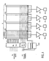
- FIG. 1 very schematically represents a memory of this type: the memory is organized in words of z bits; there are z output pads (P0 to P3), z read amplifiers (A0 to A3), z sets of columns each corresponding to an amplifier and a respective pad. Each set has p columns of cells. Finally, each column has n cells, that is to say that the memory has n rows of cells.
- a line decoder DL intended to receive a line address AL and to select a row among n as a function of this address.
- a column decoder intended to receive a column address AC and to select a column from p as a function of this address.
- the selection of a column address does not designate a single column but a column in each of the z sets and connects this column to the sense amplifier and therefore to the corresponding output pad.
- the application of a row address and a column address therefore establishes a z-bit word from z columns on the outputs. These z columns are distributed in the z sets; they all occupy the same rank (among p possible ranks) in the different sets.
- the column address actually designates a determined rank among p, for all the sets simultaneously.
- the memory can include redundant rows (not shown since we are only interested in this invention in column redundancy) and redundant columns; for example, a group of redundant columns is provided for each of the z sets.
- the groups of redundant columns are controlled by a redundancy activation circuit CAR. This circuit receives the column addresses AC, checks whether they correspond to a defective column address, and, if so, deactivates the column decoder DC and selects a redundancy column to replace it.
- the selection circuit is arranged for the selection circuit to designate a redundancy column simultaneously in each of the groups CR0 to CR3 (just as the column decoder DC simultaneously selects a column of each set). But that means that when a column is defective, in a determined set, we replace not only this column but all the columns having the same column address and being part of the other sets.
- redundancy is similar but is complicated in memories organized differently, and in particular memories which, because of their high storage capacity and their integration density, include several read amplifiers (2 or 4 or even more) by data pad. An address bit (or 2 or more) is reserved for the selection of the sense amplifier.
- the set of columns associated with each pad is now divided into several groups each corresponding to a respective amplifier.
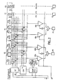
- FIG. 2 Such a memory is shown in FIG. 2.
- the organization of the rows and the line decoder are not shown, since only the arrangement of the columns concerns the redundancy of columns.
- the groups are designated by G0a and G0b for the first set E0, and by G1a and G1b for the second set E1, etc.
- the amplifiers are designated by A0a and A0b for the first set E0, and by A1a and A1b for the second, etc.
- Each group has p columns.
- the application of a word to the z memory outputs is done by selecting a row address AL, a column address AC, and a post-selection address AP.
- the line address AL designates a row of cells;
- the column address AC designates one column among p in each group, that is to say in total k times z columns, all the columns having the same rank among p rows in their respective set;
- the post selection address AP defines an amplifier rank among k in each set, or, which amounts to the same thing, a group rank of columns among k group ranks in a set; this results in the selection of an amplifier among k in each set, that is to say z amplifiers in total all having the same rank among k ranks.
- a word of z bits from columns having all the same rank (defined by AC) in the groups to which they belong will be transmitted to the data pads.
- the groups all having the same rank (defined by AP) in the sets to which they belong.
- a respective group of redundancy columns CR0a, CR0b to CR3a, CR3b is provided.
- Each group of redundancy columns comprises r columns, which means that with a group it is possible to repair a priori r defective columns.
- the architecture does not allow, as we will see, to repair a total number of columns of z times k times r (z.k.r), although there are 2 times k times r columns of redundancy.
- FIG. 2 indicates the overall constitution of the redundancy column selection circuit: it includes a comparator (COMP) receiving the address of column AC and comparing this address with addresses stored in a register for storing addresses of defective columns ( RS). If there is a coincidence, the comparator deactivates the DC column decoder to prevent it from selecting the defective column and activates a redundant column selection circuit CSR. The latter selects, according to the result of the comparison, one of the r redundancy columns of each set, simultaneously for all sets. All the redundancy columns of the same rank (among r possible rows) of the various groups CR0a, CR0b to CR3a, CR3b are therefore selected.
- COMP comparator
- the address storage register RS comprises a maximum of r memories, each making it possible to store the address of a column among p.
- the address actually stored is the AC column address of a defective column, regardless of the group to which it belongs. All the columns having the same address of column AC are replaced by redundancy columns having the same rank among r. There are z.k replacements for a defective column.
- the second is to ensure that the redundancy selection circuit is able to select any redundancy column indifferently and to route it to any amplifier, without necessarily selecting a column simultaneously in all the groups.
- this solution uses a lot of routing circuits, precisely at places close to the column outlets where there is not much room.
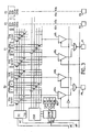
- FIG. 3 a third possible solution is shown in FIG. 3. It consists in using a selection circuit CSR which separately controls the redundancy columns of the k different groups.
- the selection circuit will designate one column among kr in each set and not one column among r in each group; only the redundancy columns which are in groups of the same rank will be selected; to illustrate this, we can say for example that the second redundant column is selected from the groups of redundant columns CR0a, CR1a, CR2a, CR3a, but without selecting the second redundant column from the other groups CR0b to CR3b.
- all the second columns of all the groups CR0a, CR0b to CR3a, CR3b were necessarily selected.
- the object of the present invention is to propose a redundancy activation circuit which allows an increase in the possibilities of repairing a memory of the type of FIG. 2 having several amplifiers per data pad.
- the improvement is of the same order as that obtained in FIG. 3 compared with FIG. 2, but it minimizes the problems of congestion by rejecting to added sparse peripheral zones the connections added in order to increase the possibilities of repair. .
- a storage register for defective addresses which comprises k groups of r zones of memory allowing each to contain a column address.
- Each group of zones corresponds to one rank of amplifier among k.
- Each group of r memory areas will be dedicated to repairing the columns of the group corresponding to an amplifier of given rank and will not be able to repair the columns corresponding to the other amplifiers and to the other column groups not having the same rank.
- the post selection address AP used to designate the rank of the amplifiers to be used and effectively used to activate all the amplifiers of this rank will also be used to designate the group of faulty address memories and to activate only the group of the row corresponding to that of the activated amplifiers.
- the selection circuit CSR remains the same as in FIG. 2 and acts in the same way on the redundant columns, but the comparator is likely to be connected to k times r memory areas (and not r areas as in FIG. 2), and the post selection address received by the memory designates a group from the k groups of memory zones so that this group is effectively connected to the comparator.
- r defective columns can be independently repaired located in groups of the same rank among k, and this for each of the rows.
- the comparator is permanently connected to k times r memory areas and must provide the selection circuit not only with one rank among r but also with one rank among k.
- the memory zones in the case of FIG. 3 must store both the column address AC and the post-selection address AF, and the comparator must provide a comparison on these two address portions.
- the comparator is only connected at a given time to r zones and not k times r, it designates a rank among r, and finally it makes comparisons only on the addresses of column AC.
- the circuit according to the invention makes it possible to reject at the periphery of the memory (where the faulty address storage registers are) the additional connections required by the increase in repair possibilities. It does not require placing switches where there would be no room, that is to say between the outputs of the columns and the amplifiers.
- a circuit for activating a redundancy column in an integrated memory with redundancy of data columns comprising:
- a network of memory elements organized in n rows and z sets of k groups of p columns, with n, z, k and p different from the unit, each set corresponding to a respective data pad among z, and each group corresponding to a respective reading amplifier among k amplifiers connected to this block, so that data from a column of a determined group in a determined set is applied to the block corresponding to this set by the amplifier corresponding to this group,
- the redundant column activation circuit being characterized in that it comprises
- a redundancy column selection circuit for selecting a redundancy column among r simultaneously in all the groups of all the sets, that is to say for simultaneously selecting zk redundancy columns of the same rank (1 among r) belonging all to different groups and sets,
- each group of memories comprising in memory r column addresses and each address making it possible to designate a column among p, each group of memories being dedicated to storing addresses of defective columns corresponding to a single row of column group among k, without distinction between the sets to which the defective columns can belong (that is to say that the first group of memories corresponds to a defective column address which belongs to the first group of any of the sets, the second group of memories corresponds to a column address belonging to the second group of columns of any set, etc.),
- a memory group selection means capable of selecting a group of memories among k during the reception by memory of a group address among k
- FIG. 4 shows a block diagram of a redundancy system according to the invention.
- each group corresponds to an amplifier, and the different amplifiers corresponding to the same set are connected to the same data output pad. There are therefore z output pads (P0 to P3 in the figure).
- the amplifiers of the first set are A0a and A0b corresponding to the groups G0a and G0b respectively, A1a and A1b corresponding to groups G1a and G1b, etc.
- the row of the column among p possible rows within a group is defined by a column address AC.
- the rank of the group or amplifier among k possible ranks within a set is defined by a post selection address AP.
- the column address selects all columns of the same rank from all groups. It makes this selection using a multiplexer placed at the outlet of the columns.
- the post selection address selects all groups of the same rank in all the sets simultaneously. This post selection is carried out by activating all the amplifiers of the same rank (1 among k) of the different sets. The activation of an amplifier connects the columns of the group corresponding to this amplifier (and more exactly the column selected in this group by the address AC) to the block of the assembly in which the group is located, block to which the 'amplifier.
- the redundancy columns can be selected using a redundancy circuit which essentially comprises a comparator COMP capable of comparing the column address AC received by the memory with addresses of defective columns stored in a storage register RS. When a defective address is applied to the memory, it is recognized by the comparator, the function of which is then to inhibit the DC column decoder and to select a redundancy column to replace the defective column.
- a redundancy circuit which essentially comprises a comparator COMP capable of comparing the column address AC received by the memory with addresses of defective columns stored in a storage register RS.
- the groups of redundancy columns are each associated with an amplifier and are connected to this amplifier via a multiplexer in the same way as the columns of memory cells. From the main network are connected to the amplifiers via a multiplexer. But while the connection of the columns of the main network is controlled by the DC decoder, the connection of the redundant columns is controlled by a selection circuit of redundant columns CSR coupled to the output of the comparator.
- the storage register comprises k groups of r memory areas, each area being able to store a column address defining a defective column (among p).
- the group in which this column is located is not identified or stored in the memory area of the storage register.
- each group of r memory areas of determined rank is intended for exclusively store a faulty column address located in a group of columns of this same rank.
- the second group includes two other areas M1b and M2b for storing defective addresses of columns located in the second rank groups G0b to G3b only.
- the register is controlled by the post selection address AP, which precisely defines rank 1 among k groups and amplifiers, and which will be used according to the invention also defines rank 1 among k of the group of storage memories of the register RS.
- the register RS Under the control of a bus PS transmitting the post selection address AP, the register RS provides the comparator COMP only with the contents of the memory areas of the group whose rank corresponds to this address. In this group there are ar memory areas, that is to say r possibilities for storing addresses of defective columns. If one precisely corresponds to the AP address received at the memory input, the comparator signals it and indicates to the selection circuit CSR which is the memory from which the detection was made.
- the selection circuit CSR is then capable, under the command of the comparator, of defining a redundancy column among r, simultaneously for all the groups of r columns of all the sets it does not make the difference between a group and another or a together and another, which minimizes the size of the multiplexer it controls (same size as in Figure 2).
- the designated redundancy column (among r) is that which corresponds to the memory (among r) which contained the defective address recognized by the comparator.
- a column from among r redundancy columns is therefore selected from each of the groups regardless of their rank among k, and it is connected to the input of the amplifier corresponding to this group. But only the activated amplifiers will effectively transmit the information to a pad. And only the amplifiers of a determined rank among k are activated, as a function of the post selection address AP. However, the detection of faulty addresses was only authorized for the columns corresponding to the same rank among k.
- the object of the invention has thus been achieved, which is to increase the possibilities of redundancy without increasing the bulk in the immediate vicinity of the columns of the memory; in particular, the size of the multiplexer which, under the control of the circuit CSR, designates one column among r, is minimized, and the added additional elements, such as the additional memory areas of the register, have been rejected towards the periphery.
- these memory zones can be constituted by batteries of fuses, or by electrically programmable memory cells such as EPROM or EEPROM cells.
Abstract
Description
L'invention concerne les mémoires réalisées en circuit-intégré et, plus particulièrement, dans une mémoire qui comporte des colonnes redondantes, un circuit d'activation de colonnes redondantes.The invention relates to memories made in integrated circuit and, more particularly, in a memory which includes redundant columns, a circuit for activating redundant columns.
Plus les mémoires ont une grande capacité de stockage et plus la technologie d'intégration est fine, plus ces mémoires sont sujettes à des défauts de fabrication. En effet, il est très difficile d'avoir à la fois une très petite taille de circuit-intégré, une très grande capacité de stockage dans cette petite taille et un bon rendement de fabrication. Un seul défaut dans une mémoire comportant un million de cellules peut entraîner la mise au rebut de la mémoire.The more the memories have a large storage capacity and the finer the integration technology, the more these memories are subject to manufacturing defects. Indeed, it is very difficult to have both a very small size of integrated circuit, a very large storage capacity in this small size and a good manufacturing yield. A single fault in a memory with one million cells can cause the memory to be discarded.
Pour augmenter le rendement de fabrication, on utilise des mémoires comportant des systèmes de redondance, c'est-à-dire comportant plus de cellules de mémoire qu'il n'est nécessaire et des circuits de connexion pour pouvoir utiliser les cellules supplémentaires ("cellules redondantes") à la place de cellules normales qui s'avèrent défectueuses. Lors du test de la mémoire, on détecte les cellules défectueuses, on établit électriquement des chemins de connexion permettant de déconnecter les cellules défectueuses et de connecter à la place des cellules redondantes, de sorte que la mémoire apparait globalement bonne à l'utilisateur malgré la présence d'éléments défectueux.To increase the production efficiency, memories are used which include redundancy systems, that is to say which include more memory cells than is necessary and connection circuits in order to be able to use the additional cells (" redundant cells ") instead of normal cells that prove to be defective. During the memory test, the defective cells are detected, electrical connection paths are established making it possible to disconnect the defective cells and to connect redundant cells instead, so that the memory appears generally good to the user despite the presence of defective elements.
Les mémoires sont organisées en principe en rangées et en colonnes de cellules; on lit sur un conducteur de colonne (parfois appelé "ligne de bit") l'information contenue dans une cellule située au carrefour de cette colonne et d'une rangée déterminée définie par une adresse de rangée.The memories are organized in principle in rows and columns of cells; we read the information on a column conductor (sometimes called "bit line") contained in a cell located at the crossroads of this column and of a determined row defined by a row address.
Les systèmes de redondance couramment utilisés ne remplacent pas en général une cellule défectueuse par une cellule redondante. Ils remplacent plus souvent une rangée ou une colonne comportant un ou plusieurs défauts par une rangée ou une colonne redondante.Commonly used redundancy systems do not generally replace a faulty cell with a redundant cell. They more often replace a row or column with one or more faults by a redundant row or column.
Pour les mémoires de grande capacité destinées à fournir des données sous forme de mots de z bits, on prévoit que le nombre de colonnes est bien supérieur à z. Par exemple on a 512 colonnes même si on veut fournir des mots de 8 ou 16 ou 32 bits à la sortie de la mémoire. Dans ce cas, les colonnes sont agencées en z ensembles de colonnes, chaque ensemble correspondant à un plot de sortie de donnée de la mémoire; sur chaque plot on recueille à chaque lecture une donnée issue d'une colonne déterminée d'un ensemble correspondant à ce plot et pas à un autre. Il y a z plots et z ensembles : un plot par ensemble.For large capacity memories intended to supply data in the form of words of z bits, it is expected that the number of columns is much greater than z. For example we have 512 columns even if we want to supply 8 or 16 or 32 bit words at the memory output. In this case, the columns are arranged in z sets of columns, each set corresponding to a data output pad from the memory; on each plot, each data item is collected from a determined column of a set corresponding to this plot and not to another. There are z studs and z sets: one stud per set.
On notera en passant que dans tout ce qui suit on considérera seulement l'aspect lecture de données contenues dans la mémoire; mais bien entendu, si la mémoire est une mémoire inscriptible électriquement (mémoire RAM ou EPROM ou EEPROM, etc.) les plots servent en même temps à introduire des données dans les cellules de mémoire pour l'écriture. Comme cela ne change rien au problème de la redondance, on ne parlera dans la suite que de lecture pour ne pas alourdir la description de l'invention. Si on doit prendre en compte également l'écriture, il suffit de rajouter les éléments nécessaires à l'écriture, et en particulier des amplificateurs d'écriture connectés entre les plots et les ensembles de colonnes.It will be noted in passing that in all that follows we will only consider the aspect of reading data contained in the memory; but of course, if the memory is an electrically writable memory (RAM or EPROM or EEPROM memory, etc.) the pads are used at the same time to introduce data into the memory cells for writing. As this does not change the problem of redundancy, we will only talk in the following about reading so as not to burden the description of the invention. If writing must also be taken into account, it suffices to add the elements necessary for writing, and in particular writing amplifiers connected between the pads and the sets of columns.
Dans les réalisations les plus simples, à chaque plot correspond un amplificateur de lecture de données mémorisées.In the simplest embodiments, each plot corresponds to an amplifier for reading stored data.
La figure 1 représente très schématiquement une mémoire de ce type : la mémoire est organisée en mots de z bits; il y a z plots de sortie (P0 à P3), z amplificateurs de lecture (A0 à A3), z ensembles de colonnes correspondant chacun à un amplificateur et un plot respectif. Chaque ensemble comporte p colonnes de cellules. Enfin, chaque colonne comporte n cellules, c'est-à-dire que la mémoire comporte n rangées de cellules.FIG. 1 very schematically represents a memory of this type: the memory is organized in words of z bits; there are z output pads (P0 to P3), z read amplifiers (A0 to A3), z sets of columns each corresponding to an amplifier and a respective pad. Each set has p columns of cells. Finally, each column has n cells, that is to say that the memory has n rows of cells.
Il y a un décodeur de ligne DL destiné à recevoir une adresse de ligne AL et à sélectionner une rangée parmi n en fonction de cette adresse. Il y a un décodeur de colonne destiné à recevoir une adresse de colonne AC et à sélectionner une colonne parmi p en fonction de cette adresse. La sélection d'une adresse de colonne ne désigne pas une seule colonne mais une colonne dans chacun des z ensembles et connecte cette colonne à l'amplificateur de lecture et donc au plot de sortie correspondant. L'application d'une adresse de ligne et d'une adresse de colonne établit donc sur les sorties un mot de z bits issu de z colonnes. ces z colonnes sont réparties dans les z ensembles; elles occupent toutes le même rang (parmi p rangs possibles) dans les différents ensembles. L'adresse de colonne désigne en fait un rang déterminé parmi p, pour tous les ensembles simultanément.There is a line decoder DL intended to receive a line address AL and to select a row among n as a function of this address. There is a column decoder intended to receive a column address AC and to select a column from p as a function of this address. The selection of a column address does not designate a single column but a column in each of the z sets and connects this column to the sense amplifier and therefore to the corresponding output pad. The application of a row address and a column address therefore establishes a z-bit word from z columns on the outputs. these z columns are distributed in the z sets; they all occupy the same rank (among p possible ranks) in the different sets. The column address actually designates a determined rank among p, for all the sets simultaneously.
La mémoire peut comporter des rangées redondantes (non représentées car on ne s'intéresse dans cette invention qu'à la redondance de colonnes) et des colonnes redondantes; on prévoit par exemple un groupe de colonnes redondantes pour chacun des z ensembles. Les groupes de colonnes redondantes, globalement désignés par les références CR0 à CR3, sont commandés par un circuit d'activation de redondance CAR. Ce circuit reçoit les adresses de colonnes AC, vérifie si elles correspondent à une adresse de colonne défectueuse, et, dans l'affirmative, désactive le décodeur de colonne DC et sélectionne une colonne de redondance en remplacement.The memory can include redundant rows (not shown since we are only interested in this invention in column redundancy) and redundant columns; for example, a group of redundant columns is provided for each of the z sets. The groups of redundant columns, generally designated by the references CR0 to CR3, are controlled by a redundancy activation circuit CAR. This circuit receives the column addresses AC, checks whether they correspond to a defective column address, and, if so, deactivates the column decoder DC and selects a redundancy column to replace it.
Compte tenu du peu de place dont on dispose dans la mémoire, on s'arrange en pratique pour que le circuit de sélection désigne une colonne de redondance simultanément dans chacun des groupes CR0 à CR3 (de même que le décodeur de colonne DC sélectionne simultanément une colonne de chaque ensemble). Mais cela veut dire que lorsqu'une colonne est défectueuse, dans un ensemble déterminé, on remplace non seulement cette colonne mais toutes les colonnes ayant la même adresse de colonne et faisant partie des autres ensembles. On pourrait prévoir une autre organisation de redondance, dans laquelle on ne remplace que la colonne défectueuse, mais cela supposerait des circuits logiques supplémentaires d'aiguillage assez complexes, qu'on n'a en général pas la place de mettre dans le circuit intégré car ils encombrent fortement la périphérie immédiate du réseau de cellules mémoire.Given the limited space available in the memory, in practice it is arranged for the selection circuit to designate a redundancy column simultaneously in each of the groups CR0 to CR3 (just as the column decoder DC simultaneously selects a column of each set). But that means that when a column is defective, in a determined set, we replace not only this column but all the columns having the same column address and being part of the other sets. We could provide another redundancy organization, in which we only replace the defective column, but that would suppose quite complex additional logic switching circuits, which we generally don't have the place to put in the integrated circuit because they heavily clutter the immediate periphery of the memory cell network.
L'organisation de la redondance est similaire mais se complique dans des mémoires organisées différemment, et en particulier des mémoires qui, en raison de leur forte capacité de stockage et de leur densité d'intégration, comportent plusieurs amplificateurs de lecture (2 ou 4 ou même plus) par plot de donnée. Un bit d'adresse (ou 2 ou plus) est réservé à la sélection de l'amplificateur de lecture. L'ensemble de colonnes associé à chaque plot est alors maintenant divisé en plusieurs groupes correspondant chacun à un amplificateur de lecture respectif.The organization of the redundancy is similar but is complicated in memories organized differently, and in particular memories which, because of their high storage capacity and their integration density, include several read amplifiers (2 or 4 or even more) by data pad. An address bit (or 2 or more) is reserved for the selection of the sense amplifier. The set of columns associated with each pad is now divided into several groups each corresponding to a respective amplifier.
Une telle mémoire est représentée à la figure 2. L'organisation des rangées et le décodeur de ligne ne sont pas représentés, puisque seul l'agencement des colonnes intéresse la redondance de colonnes.Such a memory is shown in FIG. 2. The organization of the rows and the line decoder are not shown, since only the arrangement of the columns concerns the redundancy of columns.
Il y a z ensembles de colonnes, désignés par E0 à E3 et correspondant chacun à un plot respectif P0 à P3. Chaque ensemble comporte K groupes (ici k=2) et chaque groupe correspond à un amplificateur respectif connecté au plot qui est associé à l'ensemble. Les groupes sont désignés par G0a et G0b pour le premier ensemble E0, et par G1a et G1b pour le deuxième ensemble E1, etc. Les amplificateurs sont désignés par A0a et A0b pour le premier ensemble E0, et par A1a et A1b pour le deuxième, etc.There are z sets of columns, designated by E0 to E3 and each corresponding to a respective pad P0 to P3. Each set has K groups (here k = 2) and each group corresponds to a respective amplifier connected to the pad which is associated with the set. The groups are designated by G0a and G0b for the first set E0, and by G1a and G1b for the second set E1, etc. The amplifiers are designated by A0a and A0b for the first set E0, and by A1a and A1b for the second, etc.
Chaque groupe comporte p colonnes. L'application d'un mot sur les z sorties de la mémoire se fait par sélection d'une adresse de ligne AL, d'une adresse de colonne AC, et d'une adresse de post-sélection AP. L'adresse de ligne AL désigne une rangée de cellules; l'adresse de colonne AC désigne une colonne parmi p dans chaque groupe, c'est-à-dire au total k fois z colonnes, toutes les colonnes ayant le même rang parmi p rangs dans leur ensemble respectif; enfin, l'adresse de post sélection AP définit un rang d'amplificateur parmi k dans chaque ensemble, ou, ce qui revient au même, un rang de groupe de colonnes parmi k rangs de groupe dans un ensemble; cela a pour conséquence la sélection d'un amplificateur parmi k dans chaque ensemble, c'est-à-dire z amplificateurs au total ayant tous le même rang parmi k rangs. Sera transmis aux plots de données un mot de z bits issu de colonnes ayant toutes le même rang (défini par AC) dans les groupes auxquels elles appartiennent, les groupes ayant eux-mêmes tous le même rang (défini par AP) dans les ensembles auxquels ils appartiennent.Each group has p columns. The application of a word to the z memory outputs is done by selecting a row address AL, a column address AC, and a post-selection address AP. The line address AL designates a row of cells; the column address AC designates one column among p in each group, that is to say in total k times z columns, all the columns having the same rank among p rows in their respective set; finally, the post selection address AP defines an amplifier rank among k in each set, or, which amounts to the same thing, a group rank of columns among k group ranks in a set; this results in the selection of an amplifier among k in each set, that is to say z amplifiers in total all having the same rank among k ranks. A word of z bits from columns having all the same rank (defined by AC) in the groups to which they belong will be transmitted to the data pads. the groups all having the same rank (defined by AP) in the sets to which they belong.
On voit sur la figure 2 comment on effectue la sélection de colonnes et la post-sélection à partir de l'adresse d'un mot qui comprend (outre l'adresse de ligne AL) les deux parties d'adresse AC et AP.We see in Figure 2 how we perform the column selection and post-selection from the address of a word which includes (in addition to the line address AL) the two address parts AC and AP.
Associé à chaque groupe de colonnes G0a, G0b à G3a, G3b, on a prévu un groupe de colonnes de redondance respectif CR0a, CR0b à CR3a, CR3b.Associated with each group of columns G0a, G0b to G3a, G3b, a respective group of redundancy columns CR0a, CR0b to CR3a, CR3b is provided.
Chaque groupe de colonnes de redondance comprend r colonnes, ce qui signifie qu'avec un groupe on peut réparer a priori r colonnes défectueuses. Toutefois, l'architecture ne permet pas, comme on va le voir de réparer un nombre total de colonnes de z fois k fois r (z.k.r), bien qu'il y ait 2 fois k fois r colonnes de redondance. En effet, pour les mêmes raisons que celles indiquées en référence à la figure 1, le circuit de sélection de colonnes de redondance va sélectionner une colonne parmi r simultanément dans tous les groupes, de sorte qu'on réparera r défauts au plus. Dans l'exemple représenté, r=2 : il y a deux colonnes de redondance dans chacun des deux groupes de chacun des quatre ensembles.Each group of redundancy columns comprises r columns, which means that with a group it is possible to repair a priori r defective columns. However, the architecture does not allow, as we will see, to repair a total number of columns of z times k times r (z.k.r), although there are 2 times k times r columns of redundancy. In fact, for the same reasons as those indicated with reference to FIG. 1, the redundancy column selection circuit will select a column from among r simultaneously in all the groups, so that at most r faults are repaired. In the example shown, r = 2: there are two redundancy columns in each of the two groups of each of the four sets.
La figure 2 indique la constitution globale du circuit de sélection de colonnes de redondance : il comporte un comparateur (COMP) recevant l'adresse de colonne AC et comparant cette adresse avec des adresses mémorisées dans un registre de stockage d'adresses de colonnes défectueuses (RS). S'il y a coïncidence, le comparateur désactive le décodeur de colonne DC pour l'empêcher de sélectionner la colonne défectueuse et active un circuit de sélection de colonne redondante CSR. Ce dernier sélectionne, en fonction du résultat de la comparaison, une des r colonnes de redondance de chaque ensemble, simultanément pour tous les ensembles. Sont donc sélectionnées toutes les colonnes de redondance de même rang (parmi r rangs possibles) des divers groupes CR0a, CR0b à CR3a, CR3b.FIG. 2 indicates the overall constitution of the redundancy column selection circuit: it includes a comparator (COMP) receiving the address of column AC and comparing this address with addresses stored in a register for storing addresses of defective columns ( RS). If there is a coincidence, the comparator deactivates the DC column decoder to prevent it from selecting the defective column and activates a redundant column selection circuit CSR. The latter selects, according to the result of the comparison, one of the r redundancy columns of each set, simultaneously for all sets. All the redundancy columns of the same rank (among r possible rows) of the various groups CR0a, CR0b to CR3a, CR3b are therefore selected.
Le registre de stockage d'adresses RS comporte au maximum r mémoires, permettant chacune de stocker l'adresse d'une colonne parmi p. L'adresse effectivement stockée est l'adresse de colonne AC d'une colonne défectueuse, indépendamment du groupe auquel elle appartient. Toutes les colonnes ayant même adresse de colonne AC sont remplacées par des colonnes de redondance ayant même rang parmi r. Il y a z.k remplacements pour une colonne défectueuse.The address storage register RS comprises a maximum of r memories, each making it possible to store the address of a column among p. The address actually stored is the AC column address of a defective column, regardless of the group to which it belongs. All the columns having the same address of column AC are replaced by redundancy columns having the same rank among r. There are z.k replacements for a defective column.
Pour augmenter les possibilités de remplacement de colonnes défectueuses, ce qui est souhaitable lorsque la taille de la mémoire augmente, il y a plusieurs solutions :To increase the possibilities of replacing defective columns, which is desirable when the memory size increases, there are several solutions:
- la première est évidemment d'augmenter r; mais cela augmente beaucoup la taille de la mémoire puisqu'il y a r fois k fois z colonnes redondantes; de plus, cela présente un risque car les colonnes redondantes elles-mêmes peuvent être défectueuses.- the first is obviously to increase r; but this greatly increases the size of the memory since there are r times k times z redundant columns; moreover, this presents a risk since the redundant columns themselves may be defective.
- la deuxième est de faire en sorte que le circuit de sélection de redondance soit capable de sélectionner indifféremment n'importe quelle colonne de redondance et de l'aiguiller vers n'importe quel amplificateur, sans sélectionner obligatoirement simultanément une colonne dans tous les groupes. Mais cette solution utilise beaucoup de circuits d'aiguillage, justement à des endroits proches des sorties de colonne où l'on n'a pas beaucoup de place.- the second is to ensure that the redundancy selection circuit is able to select any redundancy column indifferently and to route it to any amplifier, without necessarily selecting a column simultaneously in all the groups. However, this solution uses a lot of routing circuits, precisely at places close to the column outlets where there is not much room.
- une troisième solution possible est représentée à la figure 3. Elle consiste à utiliser un circuit de sélection CSR qui commande séparément les colonnes de redondance des k différents groupes. Le circuit de sélection va désigner une colonne parmi k.r dans chaque ensemble et non une colonne parmi r dans chaque groupe; seules seront sélectionnées les colonnes de redondance qui sont dans des groupes de même rang; pour illustrer cela, on peut dire par exemple qu'on sélectionne la deuxième colonne redondante des groupes de colonnes redondantes CR0a, CR1a, CR2a, CR3a, mais sans sélectionner pour autant la deuxième colonne redondante des autres groupes CR0b à CR3b. A la figure 2, on sélectionnait nécessairement toutes les deuxièmes colonnes de tous les groupes CR0a, CR0b à CR3a, CR3b. On multiplie donc en gros par k les possibilités de redondance, sans augmenter le nombre total de colonnes redondantes. Mais là encore, la réalisation est difficile par suite du peu de place dont on dispose à proximité immédiate du réseau de cellules et des décodeurs. Le comparateur, le circuit de sélection CSR sont plus compliqués, et il faut au moins k fois r lignes de sortie pour le circuit CSR au lieu de r lignes seulement.- a third possible solution is shown in FIG. 3. It consists in using a selection circuit CSR which separately controls the redundancy columns of the k different groups. The selection circuit will designate one column among kr in each set and not one column among r in each group; only the redundancy columns which are in groups of the same rank will be selected; to illustrate this, we can say for example that the second redundant column is selected from the groups of redundant columns CR0a, CR1a, CR2a, CR3a, but without selecting the second redundant column from the other groups CR0b to CR3b. In FIG. 2, all the second columns of all the groups CR0a, CR0b to CR3a, CR3b were necessarily selected. We therefore multiply roughly by k the possibilities of redundancy, without increasing the total number of redundant columns. But here again, the realization is difficult due to the little space available in the immediate vicinity of the cell network and the decoders. The comparator and the CSR selection circuit are more complicated, and at least k times r output lines are required for the CSR circuit instead of r lines only.
La présente invention a pour but de proposer un circuit d'activation de redondance qui permette une augmentation des possibilités de réparation d'une mémoire du type de la figure 2 ayant plusieurs amplificateurs par plot de donnée. L'amélioration est du même ordre que celle obtenue à la figure 3 par rapport à la figure 2, mais elle minimise les problèmes d'encombrement en rejetant vers des zones périphériques peu encombrées les connexions rajoutées en vue de l'augmentation des possibilités de réparation.The object of the present invention is to propose a redundancy activation circuit which allows an increase in the possibilities of repairing a memory of the type of FIG. 2 having several amplifiers per data pad. The improvement is of the same order as that obtained in FIG. 3 compared with FIG. 2, but it minimizes the problems of congestion by rejecting to added sparse peripheral zones the connections added in order to increase the possibilities of repair. .
Selon l'invention, on propose essentiellement d'utiliser un registre de stockage des adresses défectueuses qui comporte k groupes de r zones de mémoire permettant de contenir chacune une adresse de colonne. Chaque groupe de zones correspond à un rang d'amplificateur parmi k. Chaque groupe de r zones de mémoire sera dédié à la réparation des colonnes du groupe correspondant à un amplificateur de rang donné et ne pourra pas réparer les colonnes correspondant aux autres amplificateurs et aux autres groupes de colonne n'ayant pas le même rang. L'adresse de post sélection AP servant à désigner le rang des amplificateurs à utiliser et servant effectivement à activer tous les amplificateurs de ce rang, servira aussi à désigner le groupe de mémoires d'adresses défectueuses et à activer uniquement le groupe du rang correspondant à celui des amplificateurs activés.According to the invention, it is essentially proposed to use a storage register for defective addresses which comprises k groups of r zones of memory allowing each to contain a column address. Each group of zones corresponds to one rank of amplifier among k. Each group of r memory areas will be dedicated to repairing the columns of the group corresponding to an amplifier of given rank and will not be able to repair the columns corresponding to the other amplifiers and to the other column groups not having the same rank. The post selection address AP used to designate the rank of the amplifiers to be used and effectively used to activate all the amplifiers of this rank, will also be used to designate the group of faulty address memories and to activate only the group of the row corresponding to that of the activated amplifiers.
Par conséquent, le circuit de sélection CSR reste le même qu'à la figure 2 et agit de la même manière sur les colonnes redondantes, mais le comparateur est susceptible d'être connecté à k fois r zones de mémoire (et non pas r zones comme à la figure 2), et l'adresse de post sélection reçue par la mémoire désigne un groupe parmi les k groupes de zones de mémoire pour que ce groupe soit effectivement connecté au comparateur.Consequently, the selection circuit CSR remains the same as in FIG. 2 and acts in the same way on the redundant columns, but the comparator is likely to be connected to k times r memory areas (and not r areas as in FIG. 2), and the post selection address received by the memory designates a group from the k groups of memory zones so that this group is effectively connected to the comparator.
Les possibilités de réparation sont aussi élevées qu'avec le circuit de la figure 3 : on peut réparer indépendamment r colonnes défectueuses situées dans des groupes de même rang parmi k, et cela pour chacun des rangs.The repair possibilities are as high as with the circuit of FIG. 3: r defective columns can be independently repaired located in groups of the same rank among k, and this for each of the rows.
Par comparaison, on notera qu'à la figure 3 le comparateur est connecté en permanence à k fois r zones de mémoire et doit fournir au circuit de sélection non seulement un rang parmi r mais aussi un rang parmi k. De plus, les zones mémoires dans le cas de la figure 3 doivent stocker à la fois l'adresse de colonne AC et l'adresse de post sélection AF, et le comparateur doit fournir une comparaison sur ces deux portions d'adresse. Dans l'invention, le comparateur n'est connecté à un moment donné qu'à r zones et non k fois r, il désigne un rang parmi r, et enfin il fait des comparaisons seulement sur les adresses de colonne AC. Par ailleurs, le circuit selon l'invention permet de rejeter à la périphérie de la mémoire (là où sont les registres de stockage d'adresses défectueuses) les connexions supplémentaires nécessitées par l'accroissement des possibilités de réparation. Il ne nécessite pas de placer des aiguillages là où on n'aurait pas de place, c'est-à-dire entre les sorties des colonnes et les amplificateurs.By comparison, it will be noted that in FIG. 3 the comparator is permanently connected to k times r memory areas and must provide the selection circuit not only with one rank among r but also with one rank among k. In addition, the memory zones in the case of FIG. 3 must store both the column address AC and the post-selection address AF, and the comparator must provide a comparison on these two address portions. In the invention, the comparator is only connected at a given time to r zones and not k times r, it designates a rank among r, and finally it makes comparisons only on the addresses of column AC. Furthermore, the circuit according to the invention makes it possible to reject at the periphery of the memory (where the faulty address storage registers are) the additional connections required by the increase in repair possibilities. It does not require placing switches where there would be no room, that is to say between the outputs of the columns and the amplifiers.
Une définition structurelle détaillée de la mémoire selon l'invention pourrait être la suivante :A detailed structural definition of the memory according to the invention could be as follows:
Un circuit d'activation d'une colonne de redondance dans une mémoire intégrée avec redondance de colonnes de données, la mémoire comportant :A circuit for activating a redundancy column in an integrated memory with redundancy of data columns, the memory comprising:
- un réseau d'éléments de mémoire organisés en n rangées et z ensembles de k groupes de p colonnes, avec n, z, k et p différents de l'unité, chaque ensemble correspondant à un plot de données respectif parmi z, et chaque groupe correspondant à un amplificateur de lecture respectif parmi k amplificateurs connectés à ce plot, de telle manière qu'une donnée d'une colonne d'un groupe déterminé dans un ensemble déterminé soit appliquée au plot correspondant à cet ensemble par l'amplificateur correspondant à ce groupe,a network of memory elements organized in n rows and z sets of k groups of p columns, with n, z, k and p different from the unit, each set corresponding to a respective data pad among z, and each group corresponding to a respective reading amplifier among k amplifiers connected to this block, so that data from a column of a determined group in a determined set is applied to the block corresponding to this set by the amplifier corresponding to this group,
- un décodeur de colonne pour sélectionner une colonne parmi p simultanément dans tous les groupes de tous les ensembles, et un moyen de post-sélection pour sélectionner un amplificateur parmi k simultanément dans tous les ensembles, en fonction de la réception par la mémoire d'une adresse de colonne parmi p adresses, et d'une adresse de groupe parmi k, cette adresse de groupe définissant un rang de groupe dans chaque ensemble, le circuit d'activation de colonne redondante étant caractérisé en ce qu'il comprenda column decoder for selecting a column among p simultaneously in all the groups of all the sets, and a post-selection means for selecting an amplifier among k simultaneously in all the sets, as a function of the reception by the memory of one column address among p addresses, and a group address among k, this group address defining a group rank in each set, the redundant column activation circuit being characterized in that it comprises
- r colonnes de redondance par groupe dans chacun des ensembles, pour remplacer au moins une colonne défectueuse dans le réseau, r supérieur ou égal à l'unité, les r colonnes de redondance d'un groupe étant reliées directement à l'amplificateur correspondant à ce groupe,- r redundancy columns per group in each of the sets, to replace at least one defective column in the network, r greater than or equal to unity, the r redundancy columns of a group being connected directly to the amplifier corresponding to this group,
- un circuit de sélection de colonne de redondance pour sélectionner une colonne de redondance parmi r simultanément dans tous les groupes de tous les ensembles, c'est-à-dire pour sélectionner simultanément z.k colonnes de redondance de même rang (1 parmi r) appartenant toutes à des groupes et des ensembles différents,a redundancy column selection circuit for selecting a redundancy column among r simultaneously in all the groups of all the sets, that is to say for simultaneously selecting zk redundancy columns of the same rank (1 among r) belonging all to different groups and sets,
- k groupes de mémoires de stockage d'adresses de colonnes défectueuses, chaque groupe de mémoires comportant en mémoire r adresses de colonne et chaque adresse permettant de désigner une colonne parmi p, chaque groupe de mémoires étant dédié au stockage d'adresses de colonnes défectueuses correspondant à un seul rang de groupe de colonnes parmi k, sans distinction entre les ensembles auxquels peuvent appartenir les colonnes défectueuses (c'est-à-dire que le premier groupe de mémoires correspond à une adresse de colonne défectueuse qui appartient au premier groupe de n'importe lequel des ensembles, le deuxième groupe de mémoires correspond à une adresse de colonne appartenant au deuxième groupe de colonnes de n'importe quel ensemble, etc.),k groups of memories for storing defective column addresses, each group of memories comprising in memory r column addresses and each address making it possible to designate a column among p, each group of memories being dedicated to storing addresses of defective columns corresponding to a single row of column group among k, without distinction between the sets to which the defective columns can belong (that is to say that the first group of memories corresponds to a defective column address which belongs to the first group of any of the sets, the second group of memories corresponds to a column address belonging to the second group of columns of any set, etc.),
- un moyen de sélection de groupe de mémoires, apte à sélectionner un groupe de mémoires parmi k lors de la réception par la mémoire d'une adresse de groupe parmi k,a memory group selection means, capable of selecting a group of memories among k during the reception by memory of a group address among k,
- un moyen pour comparer une adresse de colonne parmi p, reçue par la mémoire, à toutes les adresses d'un groupe de mémoires sélectionné, et pour d'une part inhiber le décodeur de colonnes (mais non le moyen de post sélection) et d'autre part commander la sélection par le circuit de sélection de colonne de redondance d'une colonne de redondance déterminée en fonction du résultat de la comparaison.a means for comparing a column address among p, received by the memory, with all the addresses of a selected memory group, and for one part inhibiting the column decoder (but not the post selection means) and on the other hand, control the selection by the redundancy column selection circuit of a redundancy column determined as a function of the result of the comparison.
D'autres caractéristiques et avantages de l'invention apparaîtront à la lecture de la description détaillée qui suit et qui est faite en référence aux dessins annexés dans lesquels :Other characteristics and advantages of the invention will appear on reading the detailed description which follows and which is given with reference to the appended drawings in which:
- les figures 1 à 3 déjà décrites, représentent des structures de mémoires et de systèmes de redondance présentant des imperfections;- Figures 1 to 3 already described, represent memory structures and redundancy systems with imperfections;
- la figure 4 représente un schéma de principe d'un système de redondance selon l'invention.- Figure 4 shows a block diagram of a redundancy system according to the invention.
On ne reviendra pas en détail sur l'arrangement matriciel général de la figure 4 : c'est le même que celui qui a été décrit en référence aux figures 2 et 3.We will not return in detail to the general matrix arrangement of FIG. 4: it is the same as that which has been described with reference to FIGS. 2 and 3.
Il y a z ensembles de k groupes de p colonnes de cellules de mémoire d'un réseau principal, et z ensembles de k groupes de r colonnes de redondance, chaque groupe de colonnes de redondance correspondant à un groupe de colonnes de cellules de mémoire du réseau principal. En outre, chaque groupe correspond à un amplificateur, et les différents amplificateurs correspondant à un même ensemble sont connectés à un même plot de sortie de donnée. Il y a donc z plots de sortie ( P0 à P3 sur la figure) . Les amplificateurs du premier ensemble sont A0a et A0b correspondant aux groupes G0a et G0b respectivement, A1a et A1b correspondant aux groupes G1a et G1b, etc.There are az sets of k groups of p columns of memory cells of a main network, and z sets of k groups of r redundancy columns, each group of redundancy columns corresponding to a group of columns of memory cells of the network main. In addition, each group corresponds to an amplifier, and the different amplifiers corresponding to the same set are connected to the same data output pad. There are therefore z output pads (P0 to P3 in the figure). The amplifiers of the first set are A0a and A0b corresponding to the groups G0a and G0b respectively, A1a and A1b corresponding to groups G1a and G1b, etc.
Le rang de la colonne parmi p rangs possibles à l'intérieur d'un groupe est défini par une adresse de colonne AC. Le rang du groupe ou de l'amplificateur parmi k rangs possibles à l'intérieur d'un ensemble est défini par une adresse de post sélection AP.The row of the column among p possible rows within a group is defined by a column address AC. The rank of the group or amplifier among k possible ranks within a set is defined by a post selection address AP.
L'adresse de colonne sélectionne toutes les colonnes de même rang de tous les groupes. Elle effectue cette sélection grâce à un multiplexeur placé en sortie des colonnes. L'adresse de post sélection sélectionne tous les groupes de même rang dans tous les ensembles simultanément. Cette post sélection est effectuée par activation de tous les amplificateurs de même rang (1 parmi k) des différents ensembles. L'activation d'un amplificateur connecte les colonnes du groupe correspondant à cet amplificateur (et plus exactement la colonne sélectionnée dans ce groupe par l'adresse AC) au plot de l'ensemble dans lequel se situe le groupe, plot auquel est raccordé l'amplificateur.The column address selects all columns of the same rank from all groups. It makes this selection using a multiplexer placed at the outlet of the columns. The post selection address selects all groups of the same rank in all the sets simultaneously. This post selection is carried out by activating all the amplifiers of the same rank (1 among k) of the different sets. The activation of an amplifier connects the columns of the group corresponding to this amplifier (and more exactly the column selected in this group by the address AC) to the block of the assembly in which the group is located, block to which the 'amplifier.
Les colonnes de redondance peuvent être sélectionnées grâce à un circuit de redondance qui comprend essentiellement un comparateur COMP capable de comparer l'adresse de colonne AC reçue par la mémoire avec des adresses de colonnes défectueuses mémorisées dans un registre de stockage RS. Lorsqu'une adresse défectueuse est appliquée à la mémoire, elle est reconnue par le comparateur dont la fonction est alors d'inhiber le décodeur de colonne DC et de sélectionner une colonne de redondance en remplacement de la colonne défectueuse.The redundancy columns can be selected using a redundancy circuit which essentially comprises a comparator COMP capable of comparing the column address AC received by the memory with addresses of defective columns stored in a storage register RS. When a defective address is applied to the memory, it is recognized by the comparator, the function of which is then to inhibit the DC column decoder and to select a redundancy column to replace the defective column.
Les groupes de colonnes de redondance sont associés chacun à un amplificateur et sont connectées à cet amplificateur par l'intermédiaire d'un multiplexeur de la même manière que les colonnes de cellules de mémoire du réseau principal sont connectées aux amplificateurs par l'intermédiaire d'un multiplexeur. Mais alors que la liaison des colonnes du réseau principal est contrôlée par le décodeur DC, la liaison des colonnes redondantes est contrôlée par un circuit de sélection de colonnes redondantes CSR couplé à la sortie du comparateur.The groups of redundancy columns are each associated with an amplifier and are connected to this amplifier via a multiplexer in the same way as the columns of memory cells. from the main network are connected to the amplifiers via a multiplexer. But while the connection of the columns of the main network is controlled by the DC decoder, the connection of the redundant columns is controlled by a selection circuit of redundant columns CSR coupled to the output of the comparator.
Le registre de stockage comprend k groupes de r zones de mémoire, chaque zone étant apte à mémoriser une adresse de colonne définissant une colonne (parmi p) défectueuse. Le groupe dans lequel se situe cette colonne n'est pas identifié ni mémorisé dans la zone de mémoire du registre de stockage. Cependant, si on définit pour chaque groupe de r zones un rang 1 parmi k comme on a défini un rang 1 parmi k pour les groupes de colonnes du réseau et pour les amplificateurs, chaque groupe de r zones de mémoire de rang déterminé est destiné à stocker exclusivement une adresse de colonne défectueuse située dans un groupe de colonnes de ce même rang.The storage register comprises k groups of r memory areas, each area being able to store a column address defining a defective column (among p). The group in which this column is located is not identified or stored in the memory area of the storage register. However, if a
Ainsi, le registre comprend dans l'exemple représenté deux groupes (k=2) de zones de mémoire, parce qu'il y a deux amplificateurs par plot. Le premier groupe comprend deux zones (r=2) désignées par M1a et M2a destinées à stocker des adresses de colonne défectueuses uniquement si ces colonnes se situent dans les groupes de premier rang G0a, G1a, G2a, G3a. Deux adresses défectueuses peuvent être stockées pour deux réparations. Le deuxième groupe comprend deux autres zones M1b et M2b pour stocker des adresses défectueuses de colonnes situées dans les groupes de deuxième rang G0b à G3b uniquement.Thus, in the example shown, the register comprises two groups (k = 2) of memory areas, because there are two amplifiers per pad. The first group comprises two zones (r = 2) designated by M1a and M2a intended to store defective column addresses only if these columns are located in the first rank groups G0a, G1a, G2a, G3a. Two faulty addresses can be stored for two repairs. The second group includes two other areas M1b and M2b for storing defective addresses of columns located in the second rank groups G0b to G3b only.
Le registre est commandé par l'adresse de post sélection AP, qui définit justement le rang 1 parmi k des groupes et amplificateurs, et qui va servir selon l'invention à définir aussi le rang 1 parmi k du groupe de mémoires de stockage du registre RS. Sous la commande d'un bus PS transmettant l'adresse de post sélection AP, le registre RS ne fournit au comparateur COMP que les contenus des zones de mémoire du groupe dont le rang correspond à cette adresse. Dans ce groupe il y a r zones de mémoires, c'est-à-dire r possibilités de stockage d'adresses de colonnes défectueuses. Si l'une correspond justement à l'adresse AP reçue à l'entrée de la mémoire, le comparateur le signale et indique au circuit de sélection CSR quelle est la mémoire à partir de laquelle la détection a été faite.The register is controlled by the post selection address AP, which precisely defines
Le circuit de sélection CSR est capable alors, sous la commande du comparateur, de définir une colonne de redondance parmi r, simultanément pour tous les groupes de r colonnes de tous les ensembles il ne fait pas la différence entre un groupe et un autre ou un ensemble et un autre, ce qui permet de réduire au minimum la taille du multiplexeur qu'il commande (même taille qu'à la figure 2). Bien entendu, on aura compris que la colonne de redondance désignée (parmi r) est celle qui correspond à la mémoire (parmi r) qui contenait l'adresse défectueuse reconnue par le comparateur.The selection circuit CSR is then capable, under the command of the comparator, of defining a redundancy column among r, simultaneously for all the groups of r columns of all the sets it does not make the difference between a group and another or a together and another, which minimizes the size of the multiplexer it controls (same size as in Figure 2). Of course, it will be understood that the designated redundancy column (among r) is that which corresponds to the memory (among r) which contained the defective address recognized by the comparator.
Lors de la détection d'une adresse défectueuse, une colonne parmi r colonnes de redondance est donc sélectionnée dans chacun des groupes quel que soit leur rang parmi k, et elle est connectée à l'entrée de l'amplificateur correspondant à ce groupe. Mais seul les amplificateurs activés transmettront effectivement l'information vers un plot. Et ne sont activés que les amplificateurs d'un rang déterminé parmi k, en fonction de l'adresse de post sélection AP. Or on n'a autorisé la détection d'adresses défectueuses que pour les colonnes correspondant au même rang parmi k. Il en résulte que même si le circuit de sélection CSR ne fait pas la différence entre les rangs des groupes, l'ensemble du système fait cette différence et établit indirectement une corrélation entre le rang parmi k du groupe qui comporte une colonne défectueuse et le rang parmi k de la colonne de redondance qui va servir à remplacer la colonne défectueuse.When a faulty address is detected, a column from among r redundancy columns is therefore selected from each of the groups regardless of their rank among k, and it is connected to the input of the amplifier corresponding to this group. But only the activated amplifiers will effectively transmit the information to a pad. And only the amplifiers of a determined rank among k are activated, as a function of the post selection address AP. However, the detection of faulty addresses was only authorized for the columns corresponding to the same rank among k. It follows that even if the CSR selection circuit does not differentiate between the ranks of the groups, the whole system makes this difference and indirectly establishes a correlation between the rank among k of the group which includes a defective column and the rank among k of the redundancy column which will be used to replace the defective column.
On a ainsi réalisé le but de l'invention qui est d'augmenter les possibilités de redondance sans augmenter l'encombrement à proximité immédiate des colonnes de la mémoire; en particulier on minimise la taille du multiplexeur qui, sous la commande du circuit CSR, désigne une colonne parmi r, et on a rejeté vers la périphérie les éléments supplémentaires rajoutés, tels que les zones de mémoire supplémentaires du registre.The object of the invention has thus been achieved, which is to increase the possibilities of redundancy without increasing the bulk in the immediate vicinity of the columns of the memory; in particular, the size of the multiplexer which, under the control of the circuit CSR, designates one column among r, is minimized, and the added additional elements, such as the additional memory areas of the register, have been rejected towards the periphery.
On notera que ces zones de mémoire peuvent être constituées par des batteries de fusibles, ou par des cellules de mémoire électriquement programmables telles que des cellules EPROM ou EEPROM.It will be noted that these memory zones can be constituted by batteries of fuses, or by electrically programmable memory cells such as EPROM or EEPROM cells.
Claims (2)
- un réseau d'éléments de mémoire organisés en n rangées et z ensembles de k groupes de p colonnes, avec n, z, k et p différents de l'unité, chaque ensemble (E0 à E3) correspondant à un plot de données respectif (P0 à P3) parmi z, et chaque groupe (G0a, G0B à G3a, G3b) correspondant à un amplificateur de lecture respectif (A0a, A0b à A3a, A3b) parmi k amplificateurs connectés à ce plot, de telle manière qu'une donnée d'une colonne d'un groupe déterminé dans un ensemble déterminé soit appliquée au plot correspondant à cet ensemble par l'amplificateur correspondant à ce groupe,
- un décodeur de colonne (DC) pour sélectionner une colonne parmi p simultanément dans tous les groupes de tous les ensembles, et un moyen de post-sélection (PS) pour sélectionner un amplificateur parmi k simultanément dans tous les ensembles, en fonction de la réception par la mémoire d'une adresse (AC) de colonne parmi p adresses et d'une adresse (AP) de groupe parmi k, le circuit de redondance étant caractérisé en ce qu'il comporte un circuit d'activation de colonnes redondantes comprenant :
- r colonnes de redondance (CR0a, CR0b à CR3a, CR3b) par groupe dans chacun des ensembles, pour remplacer au moins une colonne défectueuse dans le réseau, r supérieur ou égal à l'unité, les r colonnes de redondance associées à un groupe étant reliées directement à l'amplificateur correspondant à ce groupe,
- un circuit (CSR) de sélection de colonne de redondance pour sélectionner une colonne de redondance parmi r simultanément dans tous les groupes de tous les ensembles, c'est-à-dire pour sélectionner simultanément z.k colonnes de redondance de même rang appartenant toutes à des groupes et des ensembles différents,
- k groupes de mémoires de stockage d'adresses de colonnes défectueuses (M1a, M1b, M2a, M2b), chaque groupe comportant en mémoire r adresses et chaque adresse permettant de désigner une colonne parmi p, chaque groupe de mémoires étant dédié au stockage d'adresses de colonnes défectueuses correspondant à un seul rang de groupe de colonnes parmi k, sans distinction entre les ensembles auxquels peuvent appartenir les colonnes défectueuses,
- un moyen de sélection (PS) de groupe de mémoires, apte à sélectionner un groupe de mémoires parmi k lors de la réception par la mémoire d'une adresse de groupe (AP) parmi k,
- un moyen (COMP) pour comparer une adresse de colonne parmi p, reçue par la mémoire, à toutes les adresses d'un groupe de mémoires sélectionné, et pour d'une part inhiber le décodeur de colonnes (mais non le moyen de post sélection) et d'autre part commander la sélection par le circuit de sélection de colonne de redondance (CSR) d'une colonne de redondance déterminée en fonction du résultat de la comparaison.Redundancy circuit according to claim 1 for a memory comprising:
- a network of memory elements organized in n rows and z sets of k groups of p columns, with n, z, k and p different from the unit, each set (E0 to E3) corresponding to a respective data pad (P0 to P3) among z, and each group (G0a, G0B to G3a, G3b) corresponding to a respective sense amplifier (A0a, A0b to A3a, A3b) among k amplifiers connected to this plot, so that data from a column of a determined group in a determined set is applied to the plot corresponding to this set by the amplifier corresponding to this group,
a column decoder (DC) for selecting a column among p simultaneously in all the groups of all the sets, and a post-selection means (PS) for selecting an amplifier among k simultaneously in all the sets, as a function of the reception by the memory of a column address (AC) among p addresses and of a group address (AP) among k, the redundancy circuit being characterized in that it comprises a circuit for activating redundant columns comprising :
- r redundancy columns (CR0a, CR0b to CR3a, CR3b) per group in each set, to replace at least one defective column in the network, r greater than or equal to unity, the r redundancy columns associated with a group being connected directly to the amplifier corresponding to this group,
a redundancy column selection circuit (CSR) for selecting a redundancy column from among r simultaneously in all the groups of all the sets, that is to say for simultaneously selecting zk redundancy columns of the same rank all belonging to different groups and sets,
k groups of memories for storing defective column addresses (M1a, M1b, M2a, M2b), each group comprising in memory r addresses and each address making it possible to designate a column among p, each group of memories being dedicated to the storage of addresses of defective columns corresponding to a single row of column group among k, without distinction between the sets to which can belong the defective columns,
a memory group selection means (PS), capable of selecting a group of memories among k during reception by the memory of a group address (AP) among k,
a means (COMP) for comparing a column address among p, received by the memory, with all the addresses of a selected memory group, and for one hand inhibiting the column decoder (but not the means of post selection) and on the other hand to control the selection by the redundancy column selection circuit (CSR) of a redundancy column determined as a function of the result of the comparison.
Applications Claiming Priority (2)
| Application Number | Priority Date | Filing Date | Title |
|---|---|---|---|
| FR8916338A FR2655763B1 (en) | 1989-12-11 | 1989-12-11 | REDUNDANCY CIRCUIT FOR MEMORY. |
| FR8916338 | 1989-12-11 |
Publications (2)
| Publication Number | Publication Date |
|---|---|
| EP0433141A1 true EP0433141A1 (en) | 1991-06-19 |
| EP0433141B1 EP0433141B1 (en) | 1992-07-01 |
Family
ID=9388355
Family Applications (1)
| Application Number | Title | Priority Date | Filing Date |
|---|---|---|---|
| EP90403478A Expired - Lifetime EP0433141B1 (en) | 1989-12-11 | 1990-12-06 | Redundancy circuit for memory |
Country Status (4)
| Country | Link |
|---|---|
| US (1) | US5504712A (en) |
| EP (1) | EP0433141B1 (en) |
| DE (1) | DE69000175T2 (en) |
| FR (1) | FR2655763B1 (en) |
Cited By (1)
| Publication number | Priority date | Publication date | Assignee | Title |
|---|---|---|---|---|
| EP0940753A2 (en) * | 1998-03-04 | 1999-09-08 | Nec Corporation | Semiconductor memory device |
Families Citing this family (5)
| Publication number | Priority date | Publication date | Assignee | Title |
|---|---|---|---|---|
| JPH09147595A (en) * | 1995-11-24 | 1997-06-06 | Nec Corp | Semiconductor storage device |
| KR100224774B1 (en) * | 1996-06-29 | 1999-10-15 | 김영환 | Column redundancy circuit of semiconductor memory |
| KR20020043796A (en) * | 2000-12-04 | 2002-06-12 | 박종섭 | Redundant circuit of semiconductor memory device |
| US20020108073A1 (en) * | 2001-02-02 | 2002-08-08 | Hughes Brian William | System for and method of operating a programmable column fail counter for redundancy allocation |
| EP1646052A1 (en) * | 2004-10-07 | 2006-04-12 | Infineon Technologies AG | A memory circuit with flexible bitline- and/or wordline-related defect memory cell substitution |
Citations (3)
| Publication number | Priority date | Publication date | Assignee | Title |
|---|---|---|---|---|
| EP0104120A2 (en) * | 1982-09-20 | 1984-03-28 | Fairchild Semiconductor Corporation | Redundant columns for byte wide memories |
| US4601019A (en) * | 1983-08-31 | 1986-07-15 | Texas Instruments Incorporated | Memory with redundancy |
| FR2611301A1 (en) * | 1987-02-24 | 1988-08-26 | Thomson Semiconducteurs | Integrated memory with data column redundancy |
Family Cites Families (3)
| Publication number | Priority date | Publication date | Assignee | Title |
|---|---|---|---|---|
| JPH01119995A (en) * | 1987-11-02 | 1989-05-12 | Toshiba Corp | Semiconductor memory |
| FR2636464B1 (en) * | 1988-09-14 | 1990-10-26 | Sgs Thomson Microelectronics | EPROM MEMORY WITH INTERNAL SIGNATURE CONCERNING IN PARTICULAR THE PROGRAMMING MODE |
| JP2664236B2 (en) * | 1989-02-01 | 1997-10-15 | 富士通株式会社 | Semiconductor storage device |
-
1989
- 1989-12-11 FR FR8916338A patent/FR2655763B1/en not_active Expired - Lifetime
-
1990
- 1990-12-06 DE DE9090403478T patent/DE69000175T2/en not_active Expired - Fee Related
- 1990-12-06 EP EP90403478A patent/EP0433141B1/en not_active Expired - Lifetime
-
1993
- 1993-07-23 US US08/097,598 patent/US5504712A/en not_active Expired - Lifetime
Patent Citations (4)
| Publication number | Priority date | Publication date | Assignee | Title |
|---|---|---|---|---|
| EP0104120A2 (en) * | 1982-09-20 | 1984-03-28 | Fairchild Semiconductor Corporation | Redundant columns for byte wide memories |
| US4601019A (en) * | 1983-08-31 | 1986-07-15 | Texas Instruments Incorporated | Memory with redundancy |
| US4601019B1 (en) * | 1983-08-31 | 1997-09-30 | Texas Instruments Inc | Memory with redundancy |
| FR2611301A1 (en) * | 1987-02-24 | 1988-08-26 | Thomson Semiconducteurs | Integrated memory with data column redundancy |
Non-Patent Citations (1)
| Title |
|---|
| IEEE JOURNAL OF SOLID-STATE CIRCUITS, vol. 24, no. 1, février 1989, pages 43-49, IEEE, New York, US; Y. NISHIMURA et al.: "A redundancy test-time reduction technique in 1-Mbit DRAM with a multibit test mode" * |
Cited By (3)
| Publication number | Priority date | Publication date | Assignee | Title |
|---|---|---|---|---|
| EP0940753A2 (en) * | 1998-03-04 | 1999-09-08 | Nec Corporation | Semiconductor memory device |
| EP0940753A3 (en) * | 1998-03-04 | 1999-09-22 | Nec Corporation | Semiconductor memory device |
| US6041006A (en) * | 1998-03-04 | 2000-03-21 | Nec Corporation | Semiconductor memory device |
Also Published As
| Publication number | Publication date |
|---|---|
| DE69000175T2 (en) | 1993-02-25 |
| FR2655763A1 (en) | 1991-06-14 |
| FR2655763B1 (en) | 1992-01-17 |
| EP0433141B1 (en) | 1992-07-01 |
| US5504712A (en) | 1996-04-02 |
| DE69000175D1 (en) | 1992-08-06 |
Similar Documents
| Publication | Publication Date | Title |
|---|---|---|
| EP0666573B1 (en) | Non volatile flip-flop, programmed via the source, especially for memory redundancy circuit | |
| FR2688328A1 (en) | Circuit with row redundancy for semiconductor memory device for repairing or replacing a defective cell of a memory cell array | |
| FR2691000A1 (en) | Column redundancy circuit for a semiconductor memory device | |
| EP0234907B1 (en) | Semiconductor memory device with redundant memory cell | |
| EP0626760B1 (en) | Electronic system organized in matrix cell network | |
| US6094385A (en) | Repairable memory cell for a memory cell array | |
| JPH07153296A (en) | Semiconductor memory | |
| FR2772507A1 (en) | INTEGRATED CIRCUIT MEMORY DEVICE HAVING DATA INPUT AND OUTPUT LINES EXTENDING IN THE DIRECTION OF THE COLUMNS, AND CIRCUITS AND METHODS FOR REPAIRING FAULTY CELLS | |
| EP0433141B1 (en) | Redundancy circuit for memory | |
| FR2611301A1 (en) | Integrated memory with data column redundancy | |
| KR100270007B1 (en) | Wordline and bitline redundancy with no performance penalty | |
| FR2576133A1 (en) | HIGH RELIABILITY INTEGRATED CIRCUIT MEMORY | |
| US6327197B1 (en) | Structure and method of a column redundancy memory | |
| EP0977120B1 (en) | Error correction in a ROM by means of redundancy | |
| WO1994006082A1 (en) | Memory circuit with redundancy architecture | |
| FR2655177A1 (en) | REDUNDANCY CIRCUIT WITH OUTPUT PLOT POSITION STORAGE. | |
| FR2680590A1 (en) | ARRANGEMENT OF A REDUNDANT CELL ARRAY FOR A SEMICONDUCTOR MEMORY DEVICE. | |
| FR2576132A1 (en) | INTEGRATED CIRCUIT MEMORY | |
| EP0675441B1 (en) | Redundancy fuses matrix array for integrated memory and implementing method | |
| JP3952259B2 (en) | DEFECT ADDRESS STORAGE CIRCUIT FOR SEMICONDUCTOR MEMORY DEVICE | |
| FR2679692A1 (en) | Semiconductor memory redundancy | |
| FR2888660A1 (en) | Column redundancy enabling system for e.g. integrated circuit memory, has controller with signal generating unit for generating signal that is conveyed to read-out circuits of memory in order to enable column redundancy unit | |
| JPH09213097A (en) | Fuse device and semiconductor integrated circuit device using the same | |
| FR2644924A1 (en) | Circuit for selecting a redundant column in an integrated memory with data column redundancy | |
| JP3352487B2 (en) | Memory with redundant memory cells |
Legal Events
| Date | Code | Title | Description |
|---|---|---|---|
| PUAI | Public reference made under article 153(3) epc to a published international application that has entered the european phase |
Free format text: ORIGINAL CODE: 0009012 |
|
| AK | Designated contracting states |
Kind code of ref document: A1 Designated state(s): DE FR GB IT |
|
| 17P | Request for examination filed |
Effective date: 19910502 |
|
| 17Q | First examination report despatched |
Effective date: 19911028 |
|
| GRAA | (expected) grant |
Free format text: ORIGINAL CODE: 0009210 |
|
| ITF | It: translation for a ep patent filed |
Owner name: AVV. ANTONIO PETRUZZELLI |
|
| AK | Designated contracting states |
Kind code of ref document: B1 Designated state(s): DE FR GB IT |
|
| REF | Corresponds to: |
Ref document number: 69000175 Country of ref document: DE Date of ref document: 19920806 |
|
| GBT | Gb: translation of ep patent filed (gb section 77(6)(a)/1977) | ||
| PLBE | No opposition filed within time limit |
Free format text: ORIGINAL CODE: 0009261 |
|
| STAA | Information on the status of an ep patent application or granted ep patent |
Free format text: STATUS: NO OPPOSITION FILED WITHIN TIME LIMIT |
|
| 26N | No opposition filed | ||
| REG | Reference to a national code |
Ref country code: FR Ref legal event code: D6 |
|
| PGFP | Annual fee paid to national office [announced via postgrant information from national office to epo] |
Ref country code: DE Payment date: 20001129 Year of fee payment: 11 |
|
| REG | Reference to a national code |
Ref country code: GB Ref legal event code: IF02 |
|
| PG25 | Lapsed in a contracting state [announced via postgrant information from national office to epo] |
Ref country code: DE Free format text: LAPSE BECAUSE OF NON-PAYMENT OF DUE FEES Effective date: 20020702 |
|
| PGFP | Annual fee paid to national office [announced via postgrant information from national office to epo] |
Ref country code: GB Payment date: 20021204 Year of fee payment: 13 |
|
| PGFP | Annual fee paid to national office [announced via postgrant information from national office to epo] |
Ref country code: FR Payment date: 20021210 Year of fee payment: 13 |
|
| PG25 | Lapsed in a contracting state [announced via postgrant information from national office to epo] |
Ref country code: GB Free format text: LAPSE BECAUSE OF NON-PAYMENT OF DUE FEES Effective date: 20031206 |
|
| GBPC | Gb: european patent ceased through non-payment of renewal fee |
Effective date: 20031206 |
|
| PG25 | Lapsed in a contracting state [announced via postgrant information from national office to epo] |
Ref country code: FR Free format text: LAPSE BECAUSE OF NON-PAYMENT OF DUE FEES Effective date: 20040831 |
|
| REG | Reference to a national code |
Ref country code: FR Ref legal event code: ST |
|
| PG25 | Lapsed in a contracting state [announced via postgrant information from national office to epo] |
Ref country code: IT Free format text: LAPSE BECAUSE OF NON-PAYMENT OF DUE FEES;WARNING: LAPSES OF ITALIAN PATENTS WITH EFFECTIVE DATE BEFORE 2007 MAY HAVE OCCURRED AT ANY TIME BEFORE 2007. THE CORRECT EFFECTIVE DATE MAY BE DIFFERENT FROM THE ONE RECORDED. Effective date: 20051206 |