EP0432368B1 - Elektrischer Steckverbinder mit einer Vorrichtung zum selbsttätigen Kurzschliessen von bestimmten Leitern bei der Abkupplung eines Steckverbinders - Google Patents
Elektrischer Steckverbinder mit einer Vorrichtung zum selbsttätigen Kurzschliessen von bestimmten Leitern bei der Abkupplung eines Steckverbinders Download PDFInfo
- Publication number
- EP0432368B1 EP0432368B1 EP90116404A EP90116404A EP0432368B1 EP 0432368 B1 EP0432368 B1 EP 0432368B1 EP 90116404 A EP90116404 A EP 90116404A EP 90116404 A EP90116404 A EP 90116404A EP 0432368 B1 EP0432368 B1 EP 0432368B1
- Authority
- EP
- European Patent Office
- Prior art keywords
- elongated conductive
- conductive elements
- past
- extends
- arm portions
- Prior art date
- Legal status (The legal status is an assumption and is not a legal conclusion. Google has not performed a legal analysis and makes no representation as to the accuracy of the status listed.)
- Expired - Lifetime
Links
Images

Classifications
-
- H—ELECTRICITY
- H01—ELECTRIC ELEMENTS
- H01R—ELECTRICALLY-CONDUCTIVE CONNECTIONS; STRUCTURAL ASSOCIATIONS OF A PLURALITY OF MUTUALLY-INSULATED ELECTRICAL CONNECTING ELEMENTS; COUPLING DEVICES; CURRENT COLLECTORS
- H01R13/00—Details of coupling devices of the kinds covered by groups H01R12/70 or H01R24/00 - H01R33/00
- H01R13/66—Structural association with built-in electrical component
- H01R13/70—Structural association with built-in electrical component with built-in switch
- H01R13/703—Structural association with built-in electrical component with built-in switch operated by engagement or disengagement of coupling parts, e.g. dual-continuity coupling part
- H01R13/7031—Shorting, shunting or bussing of different terminals interrupted or effected on engagement of coupling part, e.g. for ESD protection, line continuity
- H01R13/7032—Shorting, shunting or bussing of different terminals interrupted or effected on engagement of coupling part, e.g. for ESD protection, line continuity making use of a separate bridging element directly cooperating with the terminals
Definitions
- This invention relates generally to an electrical connector and receptacle assembly in which selected pins or conductive elements of the connector are automatically shorted upon disconnection.
- a primary object of this invention to provide an electrical connector-receptacle arrangement in which a connector member of the type having a plurality of spaced apart conductive elements or pins operates in a simple and economical manner to short a select number of its pins upon its disconnection from a complementary receptacle member.
- the invention accordingly comprises a system possessing a construction, combination of elements and arrangement of parts which are exemplified in the following detailed disclosure.
- An electrical connector and receptacle assembly comprises a connector member configured to define a first substantially planar surface.
- a plurality of elongated conductive elements or pins extend outward from the planar surface in substantially parallel spaced apart insulated relation with respect to each other.
- a receptacle member is provided for mating connection with the connector member and is configured to define a second substantially planar surface.
- a plurality of elongated receptacles extend inward from the second planar surface in substantially parallel spaced apart relation with respect to each other and in complementary receiving relation with respect to the elongated conductive elements or pins so as to accommodate insertion of the elongated conductive elements or pins into respective ones of the receptacles.
- a shorting member comprises a thin conductive sheet having a base portion fixedly connected with respect to the connector member in spaced relation with respect to each of the elongated conductive elements.
- a plurality of thin elongated arm portions are each integrally connected at one end to the base portion and cantilevered therefrom so as to extend past at least a respective one of the elongated conductive elements or pins with the other end of each arm portion extending laterally outward so as to be in contacting relation with respect to a select side of that elongated conductive element or pin past which its respective arm portion extends.
- Each of the arm portions has an inherent resilient bias so as to urge its other laterally extending end away from the first planar surface and into electrically contacting engagement with the select side of that elongated conductive element or pin past which that arm portion extends.
- the insertion of the elongated conductive elements or pins of the connector member into the complementary receptacles of the receptacle member operate to bring the second planar surface of the receptacle member into engagement with the laterally extending other ends of the arm portions so as to deflect the arm portions against the inherent resilient bias towards the first planar surface and out of electrical connection to respective ones of the elongated conductive elements or pins.
- the elongated conductive elements or pins and complementary receptacles are arranged in respective spaced apart linear relation.
- a first one of the arm portions extends past at least two of the linearly spaced apart elongated conductive elements or pins and the other end of the first arm portion extends laterally outward so as to be resiliently biased into electrical contact with the select side of the last elongated conductive element or pin past which that first arm portion extends.
- a second one of the arm portions overlies the first arm portion and extends past at least one of the linearly spaced apart conductive elongated elements or pins but not past the last elongated conductive element or pin past which the first one of said arm portions extends and the other end of the second arm portion extends laterally outward so as to be resiliently biased into electrical contact with the select side of the last elongated conductive element or pin past which the second arm portion extends.
- Insertion of the elongated conductive elements or pins of the connector member into the complementary receptacles of the receptacle member operate to bring the second planar surface of the receptacle member into engagement with the laterally extending other ends of the first and second arm portions so as to deflect the arm portions against their inherent resilient bias, towards the first planar surface and out of electrical connection to respective ones of the elongated conductive elements or pins.
- the elongated conductive elements or pins and complementary receptacles are arranged, respectively, in a spaced apart circumferential relationship.
- the base portion of the shorting member is fixedly connected within the area bounded by the circumferentially spaced apart elongated conductive elements or pins.
- a first one of the arm portions extends from the area bounded by the circumferentially spaced apart elongated conductive elements or pins past a first one of the elongated conductive elements or pins and the other end of the first arm portion extends laterally outward so as to be resiliently biased into electrical contact with the select side of the first elongated conductive element or pin.
- a second one of the arm portions extends from the area bounded by the circumferentially spaced apart elongated conductive elements or pins past a second one of the elongated conductive elements or pins and the other end of the second arm portion extends laterally outward so as to be resiliently biased into electrical contact with the select side of the second elongated conductive element or pin.
- Insertion of the elongated conductive elements or pins of the connector member into the complementary receptacles of the receptacle member operate to bring the second planar surface of receptacle member into engagement with the laterally extending other ends of the first and second arm portions so as to deflect the arm portions against their inherent resilient bias towards the first planar surface and out of electrical connection to the first and second elongated conductive leads, respectively.
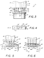
- the connector member 12 in one embodiment may comprise a generally cylindrical housing 14 having a substantially planar surface 16 at one end thereof.
- a plurality of elongated conductive elements or pins 18 extend from the planar surface 16 in substantially parallel, spaced apart, insulated relation with respect to each other.
- the conductive elements or pins 18 are preferably circumferentially disposed with respect to each other so as to define a circular arrangement.
- the housing 14 may house a single electrical component such as an integrated circuit, a laser, a light emitting diode, etc., or a plurality of such electrical components.
- the housing 14 may simply house the electrical connection between the conductive elements or pins 18 and a plurality of corresponding lead wires which ultimately connect to other electrical components remotely stationed with respect to the connector housing 14 in a well-known manner.
- the connector member 12 is adapted for ready insertion or withdrawal from the complementary receptacle member 20 which comprises a housing 22 defining a substantially planar surface 24 on one select face thereof.
- a plurality of elongated receptacles 26 extend inward from the planar surface 24 in substantially parallel spaced apart insulated relation with respect to each other and in complementary relation with respect to the elongated conductive elements or pins 18 so as to accommodate ready insertion of the elongated conductive elements or pins 18 into respective ones of the receptacles 26.
- connection of the connector member 12 to the receptacle member 20 by insertion of the elongated conductive elements or pins 18 into respective corresponding ones of the receptacles 26 operates to bring the planar surface 16 of the connector member 12 into overlapping substantially contiguous relation with respect to the substantially planar surface 24 of the receptacle member 20.
- the receptacle member housing 22 aside from the planar surface 24 may have any convenient shape or form and may operate to house either a single electrical component or a plurality of electrical components such as previously recited with respect to the connector housing 14. Alternatively, the receptacle housing 22 may simply operate to house a plurality of connections between the receptacles 26 and corresponding lead wires which ultimately connect to other electrical components remotely stationed with respect to the receptacle housing 22.
- a shorting member as shown generally at 28 comprising a thin conductive sheet having a base portion 30 fixedly connected in overlying relationship with respect to the planar surface 16 of the connector member 12 and in spaced relation with respect to the conductive elements 18.
- the base portion 30 of the connector member 12 although preferably residing within the area bounded by the circumferentially spaced apart elongated conductive elements or pins 18, as shown, can alternatively be outside this area.
- the thin conductive sheet of the shorting member 28 is cut to define a plurality of thin elongated arm portions two of which are shown at 32A and 32B.
- the arm portions 32A and 32B are cantilevered from the base portion 30 so as to extend past at least a respective one of the elongated conductive elements or pins 18A and 18B.
- the other end of the arm portions 32A and 32B extend laterally outward as shown at 34A and 34B so as to be in respective electrically contacting relation with respect to a select side of the conductive elements 18A and 18B past which said arm portions 32A and 32B respectively extend.
- the arm portions 32A and 32B have an inherent resilient spring bias so as to urge their respective laterally extending ends 34A and 34B away from the planar surface 16 and into respective electrically contacting engagement with the select sides of the elongated conductive elements 18A and 18B past which the arm portions 32A and 32B respectively extend.
- arm portions 32A and 32B spring upward such that the laterally extending end portions 34A and 34B thereof respectively engage conductive elements or pins 18A and 18B so as to establish an electrical connection therebetween by way of the shorting member 28.
- the shorting of select conductive elements or pins is accomplished so as to effect protection from static shock which can operate to damage electrical components connected thereto.
- Insertion of the conductive elements 18 of the connector member 12 into the complementary receptacles 26 of the receptacle member 20 operates to move the planar surface 24 into engagement with the laterally extending ends 34A and 34B so as to break their electrical connection with conductive elements or pins 18A and 18B, respectively, and thereafter move their respective arm portions 32A and 32B against the force of their inherent resilient spring bias toward the planar surface 16 of the electrical connector member 12.
- the inherent resilient spring biased arm portions 32A and 32B are substantially flattened between the planar surface 16 of the electrical connector 12 and the planar surface 24 of the receptacle member 20 so as to be out of electrical contact with any of the conductive elements or pins 18.
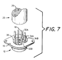
- the number of conductive elements of the connector member 12 to be shorted by the shorting member 28 is not just limited to the opposing pins 18A and 18B as shown at FIGS. 1 - 3 but may also include adjacent pins as shown in the embodiment of FIG. 7 where like numerals designate previously described elements.
- the shorting member 28 is not limited to having only two shorting arm portions but may have any select number of arm portions extending past respective corresponding conductive elements so as to effectively short any select number of conductive elements upon disconnection of the connector member from the receptacle member.
- the shorting member 28 may comprise any metallized foil and may be fixedly connected with respect to the planar surface 16 of the connector member 12 by any conventional means such as a suitable adhesive or by tack welding.
- FIGS. 4 - 6 where like numerals designate previously described elements, there is shown an alternate embodiment for the electrical connector and receptacle assembly 10′ of this invention.
- the plurality of elongated conductive elements or pins 18 are arranged in linear spaced apart relationship with respect to each other.
- the connector member 12′ further comprises a rectangularly shaped housing 14′ having a substantially planar surface 16′ and a plurality of depending side surfaces 36′ substantially orthogonal to the planar surface 16′.
- the shorting member as shown generally at 28′ comprises two overlapping thin conductive sheets each having base portions 30′ and 30 ⁇ , respectively, fixedly connected in contiguous relationship with respect to each other and the side surface 36′.
- an arm portion 32′ which extends past the conductive elements or pins 18A, 18B and 18C with the laterally extending end 34′ thereof engaging a side of the conductive element or pin 18A.
- a second arm portion 32 ⁇ extending past the conductive element or pin 18C with the laterally extending end portion 34 ⁇ thereof electrically contacting a select side of the conductive element or pin 18C.
- the laterally extending end portions 34′ and 34 ⁇ of the spring biased arm portions 32′ and 32 ⁇ engage respectively the conductive elements or pins 18A and 18C so as to create an electrical short by way of the contacting base portions 30′ and 30 ⁇ .
- Insertion of the conductive elements or pins 18 of the connector member 12 into the complementary receptacles 26′ of the receptacle member 20′ operate to move the planar surface 24′ of the receptacle member 20′ into engagement with the laterally extending portions 34′ and 34 ⁇ so as to break the electrical connection to their respective conductive elements or pins 18A and 18C.
- Complete insertion of the connector member 12′ with respect to the receptacle member 20′ operates to substantially flatten the arm portions 32′ and 32 ⁇ of the shorting member 28′ between the planar surfaces 16′ and 24′ thereby electrically disconnecting the short between the conductive elements or pins 18A and 18C.
Claims (8)
- Elektrischer Steckverbinder, bestehend aus einem Stiftstecker (12), der eine ebene Oberfläche (16) definiert, und aus mehreren langgestreckten leitfähigen Elementen (18), die von der ebenen Oberfläche (16) im wesentlichen parallel und im Abstand zueinander und gegeneinander isoliert vorstehen, und aus einem Kurzschlußglied,
dadurch gekennzeichnet, daß das Kurzschlußglied aus einem dünnen leitfähigen Blech besteht, dessen Basisabschnitt (30) fest mit dem Stiftstecker (12) im Abstand zu jedem leitfähigen Element (18) angeordnet ist und das mehrere dünne langgestreckte Armabschnitte (32A, 32B) aufweist, die jeweils integral mit einem Ende des Basisabschnitts (30) verbunden sind und auslegerartig hiervon derart vorstehen, daß sie sich wenigstens an einem der langgestreckten Elemente (18) vorbei erstrecken, während das andere Ende eines jeden Armabschnitts (34A, 34B) seitlich nach außen derart vorsteht, daß es eine elektrische Kontaktverbindung mit einer gewählten Seite jenes langgestreckten leitfähigen Elementes (18) herstellt, an welchem sich der Armabschnitt (34A, 34B) vorbei erstreckt, und daß jeder Armabschnitt (32A, 32B) eine elastische Eigenvorspannung besitzt, derart, daß das andere seitlich verlaufende Ende (34A, 34B) von der ebenen Oberfläche (16) weggedrängt und in Kontaktberührung mit der gewählten Seite des langgestreckten leitfähigen Elementes (18) gebracht wird, an dem sich der Armabschnitt (34A, 34B) vorbei erstreckt. - Elektrischer Steckverbinder nach Anspruch 1, bei welchem die langgestreckten leitfähigen Elemente (18) im Abstand zueinander in einer linearen Reihe zueinander angeordnet sind, wobei ein erster der Armabschnitte (32′) sich an wenigstens zwei der in linearem Abstand zueinander befindlichen langgestreckten Leiterelemente vorbei erstreckt und das andere Ende des ersten Armabschnitts sich seitlich nach außen derart erstreckt, daß es elastisch in elektrische Kontaktberührung mit der gewählten Seite des letzten langgestreckten leitfähigen Elementes (18) gelangt, an dem der erste Armabschnitt vorbeiläuft, während ein zweiter Armabschnitt (32˝) über dem ersten Armabschnitt (32′) liegt und sich an wenigstens einem der linear im Abstand zueinander angeordneten leitfähigen langgestreckten Elemente (18) vorbei erstreckt, an dem der erste Armabschnitt (32) vorbeiläuft, und wobei das andere Ende des zweiten Armabschnitts seitlich nach außen derart vorsteht, daß es elastisch in elektrische Kontaktberührung mit der gewählten Seite des letzten langgestreckten leitfähigen Elementes (18) vorgespannt ist, an dem der zweite Armabschnitt (32˝) vorbeiläuft.
- Elektrischer Steckverbinder nach Anspruch 2, bei welchem der Kuppler (12′) ein Gehäuse mit einer ersten Oberfläche aufweist, die die ebene Oberfläche (16′) definiert, von der die langgestreckten leitfähigen Elemente (18) vorstehen, wobei mehrere seitlich herabstehende Oberflächen (14′) im wesentlichen senkrecht zu der ersten Oberfläche (16′) verlaufend angeordnet sind, während ein Basisteil (30) des Kurzschlußgliedes fest mit einer gewählten Seitenoberfläche (14′) verbunden ist.
- Elektrischer Steckverbinder nach Anspruch 1, bei welchem die langgestreckten leitfähigen Elemente (18) im Abstand zueinander und in Umfangsrichtung angeordnet sind und der Basisabschnitt (30) des Kurzschlußgliedes fest innerhalb des Bereiches verbunden ist, der durch die in Umfangsrichtung im Abstand zueinander angeordneten langgestreckten leitfähigen Elemente (18) umschlossen ist, wobei ein erster Armabschnitt (32A) von dem Bereich vorsteht, der durch die in Umfangsrichtung im Abstand zueinander angeordneten langgestreckten leitfähigen Elemente (18) an einem ersten der langgestreckten leitfähigen Elemente (18) vorbeiläuft, während das andere Ende des ersten Armabschnitts (32A) seitlich nach außen derart vorsteht, daß es elastisch in elektrische Kontaktberührung mit der gewählten Seite des ersten langgestreckten leitfähigen Elementes (18) gebracht wird, während ein zweiter Armabschnitt (32B) von dem Bereich vorsteht, der durch die in Umfangsrichtung im Abstand zueinander angeordneten langgestreckten leitfähigen Elemente (18) umschlossen ist, wobei dieser Armabschnitt an einem zweiten der langgestreckten leitfähigen Elemente (18) vorbeiläuft, während das andere Ende (34B) des zweiten Armabschnitts seitlich derart verläuft, daß es elastisch in elektrische Kontaktberührung mit der gewählten Seite des zweiten langgestreckten leitfähigen Elementes (18) gebracht wird.
- Steckverbindungskupplung, bestehend aus Stiftstecker und Kuppler, mit den folgenden Merkmalen:- ein Stiftstecker (12) definiert eine im wesentlichen ebene Oberfläche (16);- mehrere langgestreckte leitfähige Elemente (18) stehen von der ersten ebenen Oberfläche (16) im wesentlichen parallel und im Abstand zueinander und gegeneinander isoliert vor;- ein Kuppler (20) definiert eine zweite, im wesentlichen ebene Oberfläche (24);- mehrere langgestreckte Buchsen (26) erstrecken sich von der zweiten ebenen Oberfläche (24) im wesentlichen parallel zueinander, im Abstand und gegeneinander isoliert komplementär zu den langgestreckten leitfähigen Elementen (18) in den Kuppler hinein, um die langgestreckten leitfähigen Elemente (18) beim Zusammenstecken aufzunehmen; und- ein Kurzschlußglied, welches aus einem dünnen leitfähigen Blech besteht, dessen Basisteil (30) fest mit dem Stiftstecker (12) im Abstand zu jedem langgestreckten leitfähigen Element (18) angeordnet ist, während mehrere dünne langgestreckte Armabschnitte (32A, 32B), die integral an einem Ende des Basisteils (30) fixiert sind, auslegerartig vorstehen, so daß sie an wenigstens einem der langgestreckten leitfähigen Elemente (18) vorbeilaufen, während das andere Ende eines jeden Armes (34A, 34B) seitlich derart nach außen verläuft, daß es in elektrisch leitfähige Verbindung mit einer gewählten Seite jenes leitfähigen Elementes (18) gelangt, an dem der Armabschnitt vorbeiläuft, und jeder Armabschnitt eine eigene elastische Vorspannung derart aufweist, daß sein anderes seitlich vorstehendes Ende (34A, 34B) von der ersten ebenen Oberfläche (16) weg und in elektrisch leitfähige Berührung mit der gewählten Seite des leitfähigen Elementes (18) gebracht wird, an dem der Armabschnitt vorbeiläuft, wobei das Einstecken der langgestreckten leitfähigen Stiftelemente (18) des Steckverbinders (12) in die komplementären Kontaktbuchsen (26) des Kupplers (20) bewirkt, daß die zweite ebene Oberfläche (24) des Kupplers (20) die seitlich verlaufenden anderen Enden (34A, 34B) der Armabschnitte berührt, derart, daß die Armabschnitte gegen ihre eigene innere Vorspannung nach der ersten ebenen Oberfläche (16) hin ausgelenkt werden und die elektrische Verbindung mit den betreffenden leitfähigen langgestreckten Elementen (18) geöffnet wird.
- Steckverbindungskupplung nach Anspruch 5, bei welcher die langgestreckten leitfähigen Elemente (18) und die komplementären Kontaktbuchsen (26) im Abstand zueinander in einer Reihe angeordnet sind und ein erster (32′) Armabschnitt sich an wenigstens zwei der linear im Abstand zueinander angeordneten leitfähigen Kontaktelemente (18′) vorbei erstreckt, während das andere Ende (34′) des ersten Armabschnitts (32′) seitlich nach außen derart vorsteht, daß es elastisch in elektrische Kontaktberührung mit der gewählten Seite des letzten langgestreckten leitfähigen Elementes (18′) gebracht wird, an dem der erste Armabschnitt (32′) vorbeiläuft, wobei ein zweiter (32˝) der Armabschnitte über dem ersten Armabschnitt (32′) läuft und an wenigstens einem der in linearem Abstand zueinander angeordneten langgestreckten leitfähigen Elemente (18) vorbeiläuft, aber nicht an dem letzten langgestreckten leitfähigen Element (18′) vorbei, an dem der erste Armabschnitt (32′) vorbeiläuft, während das andere Ende (34˝) des zweiten Armabschnitts (32′) seitlich nach außen derart vorsteht, daß es elastisch in elektrische Kontaktverbindung mit der gewählten Seite des letzten langgestreckten Elementes (18′) gebracht wird, an dem der zweite Armabschnitt (32˝) vorbeiläuft, wobei beim Einstecken der langgestreckten elektrischen Stiftelemente (18′) des Stiftsteckers (12′) in die komplementären Kontaktbuchsen (26′) des Kupplers (20′) bewirkt wird, daß die zweite ebene Oberfläche (24′) des Kupplers (20) in Eingriff mit den seitlich verlaufenden anderen Enden (34′, 34˝) des ersten und zweiten Armabschnitts (32′, 32˝) gelangt, so daß die Armabschnitte (32′, 32˝) gegen ihre eigene elastische Vorspannung nach der ersten ebenen Oberfläche (16′) gedrückt werden und die elektrische Verbindung mit den langgestreckten leitfähigen Elementen (18′) unterbrochen wird.
- Steckverbindungskupplung nach Anspruch 6, bei welcher der Stiftstecker (12′) ein Gehäuse mit einer ersten Oberfläche aufweist, die die ebene Oberfläche (16′) bildet, von der die langgestreckten leitfähigen Elemente (18) vorstehen, wobei mehrere seitlich herablaufende Seitenoberflächen (14′) im wesentlichen senkrecht zu der ersten Oberfläche (16′) verlaufen und der Basisabschnitt (30′) des Kurzschlußgliedes fest mit einer der Seitenflächen (14′) verbunden ist.
- Steckverbindungskupplung nach Anspruch 5, bei welcher die langgestreckten leitfähigen Elemente (18) und die komplementären Kontaktbuchsen (26) im Abstand zueinander in Umfangsrichtung angeordnet sind, wobei der Basisabschnitt (30) des Kurzschlußgliedes fest innerhalb des Bereichs angeordnet ist, der von den in Umfangsrichtung im Abstand zueinander liegenden langgestreckten Kontaktelementen (18) umschlossen wird, wobei ein erster Armabschnitt (32A) aus dem Bereich vorsteht, der durch die in Umfangsrichtung im Abstand zueinander angeordneten langgestreckten leitfähigen Elemente (18) definiert ist, und sich dieser erste Armabschnitt (32A) an einem ersten der langgestreckten leitfähigen Elemente (18) vorbei erstreckt und das andere Ende (34A) des ersten Armabschnitts (32A) seitlich nach außen derart vorsteht, daß es elastisch in elektrische Kontaktverbindung mit der gewählten Seite des ersten langgestreckten leitfähigen Elementes (18) gelangt, während ein zweiter Armabschnitt (32B) von dem Bereich, der von den in Umfangsrichtung im Abstand zueinander angeordneten langgestreckten leitfähigen Elementen (18) bestimmt wird, an einem zweiten langgestreckten leitfähigen Element (18) vorbeiläuft und das andere Ende (34B) des zweiten Armabschnitts (32B) seitlich nach außen derart verläuft, daß es elastisch in elektrische Kontaktberührung mit der gewählten Seite des zweiten langgestreckten leitfähigen Elementes (18) gelangt, so daß beim Einstecken der langgestreckten leitfähigen Stiftelemente (18) des Stiftsteckers (12) in die komplementären Kontaktbuchsen (26) des Kupplers (20) die zweite ebene Oberfläche (24) des Kupplers (20) in Berührung mit den seitlich verlaufenden anderen Enden (34A, 34B) des ersten und zweiten Armabschnitts (32A, 32B) gebracht wird, so daß die Armabschnitte (32A, 32B) gegen die ihnen eigene elastische Vorspannung nach der ersten ebenen Oberfläche (16) hin ausgelenkt werden und die elektrische Verbindung mit den ersten und zweiten Leitern (18) unterbrochen wird.
Applications Claiming Priority (2)
| Application Number | Priority Date | Filing Date | Title |
|---|---|---|---|
| US07/448,228 US4971568A (en) | 1989-12-11 | 1989-12-11 | Electrical connector with attachment for automatically shorting select conductors upon disconnection of connector |
| US448228 | 1989-12-11 |
Publications (2)
| Publication Number | Publication Date |
|---|---|
| EP0432368A1 EP0432368A1 (de) | 1991-06-19 |
| EP0432368B1 true EP0432368B1 (de) | 1994-11-09 |
Family
ID=23779475
Family Applications (1)
| Application Number | Title | Priority Date | Filing Date |
|---|---|---|---|
| EP90116404A Expired - Lifetime EP0432368B1 (de) | 1989-12-11 | 1990-08-27 | Elektrischer Steckverbinder mit einer Vorrichtung zum selbsttätigen Kurzschliessen von bestimmten Leitern bei der Abkupplung eines Steckverbinders |
Country Status (8)
| Country | Link |
|---|---|
| US (1) | US4971568A (de) |
| EP (1) | EP0432368B1 (de) |
| JP (1) | JPH088130B2 (de) |
| AT (1) | ATE114080T1 (de) |
| CA (1) | CA2021889A1 (de) |
| DE (1) | DE69014082T2 (de) |
| DK (1) | DK0432368T3 (de) |
| ES (1) | ES2066920T3 (de) |
Cited By (1)
| Publication number | Priority date | Publication date | Assignee | Title |
|---|---|---|---|---|
| US5653606A (en) * | 1994-11-18 | 1997-08-05 | The Whitaker Corporation | Electrical interconnection system having retention and shorting features |
Families Citing this family (20)
| Publication number | Priority date | Publication date | Assignee | Title |
|---|---|---|---|---|
| US5163850A (en) * | 1991-04-18 | 1992-11-17 | Polaroid Corporation | Electrostatic discharge protection devices for semiconductor chip packages |
| US5108299A (en) * | 1991-04-18 | 1992-04-28 | Polaroid Corporation | Electrostatic discharge protection devices for semiconductor chip packages |
| DE4118312C2 (de) * | 1991-06-04 | 1995-03-09 | Amphenol Tuchel Elect | Kontaktsatz für eine Kontaktzonen aufweisende Karte |
| JPH089915Y2 (ja) * | 1991-07-15 | 1996-03-21 | 日本航空電子工業株式会社 | スイッチ付きコネクタ |
| US5401180A (en) * | 1993-06-01 | 1995-03-28 | Itt Corporation | Connector shorting spring |
| US5490033A (en) * | 1994-04-28 | 1996-02-06 | Polaroid Corporation | Electrostatic discharge protection device |
| US5599205A (en) * | 1994-07-20 | 1997-02-04 | Polaroid Corporation | Electrostatic discharge protection device |
| US5583733A (en) * | 1994-12-21 | 1996-12-10 | Polaroid Corporation | Electrostatic discharge protection device |
| EP0734100B1 (de) * | 1995-03-20 | 2003-05-07 | The Whitaker Corporation | Elektrischer Steckverbinder mit versicherter Endposition |
| US5609498A (en) * | 1995-09-19 | 1997-03-11 | Itt Corporation | Secure connector system |
| US5847914A (en) * | 1995-12-21 | 1998-12-08 | Polaroid Corporation | Electrostatic discharge protection device |
| US5697501A (en) * | 1995-12-21 | 1997-12-16 | Polaroid Corporation | Electrostatic discharge protection device |
| US5812357A (en) * | 1996-10-11 | 1998-09-22 | Polaroid Corporation | Electrostatic discharge protection device |
| US5877933A (en) * | 1997-04-16 | 1999-03-02 | Johansen; Arnold W. | Electrostatic discharge protection device for magnetoresistive head |
| US5963415A (en) * | 1997-07-05 | 1999-10-05 | Polaroid Corporation | Electrostatic discharge protection device |
| US6065985A (en) * | 1998-10-14 | 2000-05-23 | Berg Technology, Inc. | Modular jack with flexible shorting structure |
| US6835079B2 (en) * | 2002-05-23 | 2004-12-28 | Positronic Industries, Inc. | Electrical connector assembly with shorting member |
| US7354287B1 (en) | 2006-10-31 | 2008-04-08 | Caterpillar Inc. | Shorting connector |
| US7789685B2 (en) * | 2006-12-18 | 2010-09-07 | Caterpillar Inc | Electrical shorting system |
| US7616421B2 (en) * | 2006-12-18 | 2009-11-10 | Caterpillar Inc. | Electrical interface system |
Family Cites Families (10)
| Publication number | Priority date | Publication date | Assignee | Title |
|---|---|---|---|---|
| US2197426A (en) * | 1936-11-05 | 1940-04-16 | Cinch Mfg Corp | Switch and radio tube socket assembly |
| US3467940A (en) * | 1967-03-17 | 1969-09-16 | William H Wallo | Electrical connecting spring device |
| US3600531A (en) * | 1970-05-08 | 1971-08-17 | Nat Tel Tronics Corp | Self-shorting phono plug |
| US3851944A (en) * | 1973-03-30 | 1974-12-03 | Okzona Inc | Current transformer connector |
| US4070557A (en) * | 1976-07-26 | 1978-01-24 | Northern Telecom Limited | Apparatus for providing closed loop conditions in vacant module positions |
| US4179178A (en) * | 1978-02-02 | 1979-12-18 | Rca Corporation | Plug-in circuit cartridge with electrostatic charge protection |
| USRE32760E (en) * | 1982-12-22 | 1988-10-04 | Amp Domestic Inc. | Electrical connector |
| US4699443A (en) * | 1984-12-28 | 1987-10-13 | American Telephone And Telegraph Company | Modular telephone jack |
| US4786258A (en) * | 1987-05-13 | 1988-11-22 | Amp Incorporated | Electrical connector with shunt |
| US4798542A (en) * | 1987-04-16 | 1989-01-17 | Amp Incorporated | Switching connector |
-
1989
- 1989-12-11 US US07/448,228 patent/US4971568A/en not_active Expired - Lifetime
-
1990
- 1990-07-24 CA CA002021889A patent/CA2021889A1/en not_active Abandoned
- 1990-08-27 DK DK90116404.6T patent/DK0432368T3/da active
- 1990-08-27 EP EP90116404A patent/EP0432368B1/de not_active Expired - Lifetime
- 1990-08-27 DE DE69014082T patent/DE69014082T2/de not_active Expired - Fee Related
- 1990-08-27 ES ES90116404T patent/ES2066920T3/es not_active Expired - Lifetime
- 1990-08-27 AT AT90116404T patent/ATE114080T1/de not_active IP Right Cessation
- 1990-10-23 JP JP2285715A patent/JPH088130B2/ja not_active Expired - Fee Related
Cited By (1)
| Publication number | Priority date | Publication date | Assignee | Title |
|---|---|---|---|---|
| US5653606A (en) * | 1994-11-18 | 1997-08-05 | The Whitaker Corporation | Electrical interconnection system having retention and shorting features |
Also Published As
| Publication number | Publication date |
|---|---|
| EP0432368A1 (de) | 1991-06-19 |
| JPH03190070A (ja) | 1991-08-20 |
| ES2066920T3 (es) | 1995-03-16 |
| CA2021889A1 (en) | 1991-06-12 |
| DE69014082D1 (de) | 1994-12-15 |
| DE69014082T2 (de) | 1995-03-23 |
| ATE114080T1 (de) | 1994-11-15 |
| DK0432368T3 (da) | 1994-12-12 |
| JPH088130B2 (ja) | 1996-01-29 |
| US4971568A (en) | 1990-11-20 |
Similar Documents
| Publication | Publication Date | Title |
|---|---|---|
| EP0432368B1 (de) | Elektrischer Steckverbinder mit einer Vorrichtung zum selbsttätigen Kurzschliessen von bestimmten Leitern bei der Abkupplung eines Steckverbinders | |
| US5240430A (en) | Electrical connector for cable to circit board application | |
| US5164880A (en) | Electrostatic discharge protection device for a printed circuit board | |
| EP0772898B1 (de) | Verbesserte erdabdeckung für elektrische verbinder | |
| EP0214830B1 (de) | Verbinder für eine biegsame gedruckte Schaltung | |
| US6165017A (en) | Cable end connector | |
| KR100367071B1 (ko) | 무선전화기크래들컨넥터 | |
| US6315620B1 (en) | System, method, and device for a pre-loaded straddle mounted connector assembly | |
| US4870753A (en) | Method of manufacturing a light socket | |
| US6099335A (en) | Electrical card connector | |
| US4934943A (en) | Automated connector alignment assembly for connection of printed circuit boards | |
| US6109952A (en) | Terminal connector assembly | |
| US4731925A (en) | Method for providing a power connector | |
| US4237435A (en) | Ground fault receptacle re-set guide assembly | |
| US5186639A (en) | Electrical connector with plug detection switch | |
| EP0540260B1 (de) | Elektrischer Verbinder zur Verbindung einer Leiterplatte mit einem Kabel | |
| US6457987B1 (en) | Plug connector with latch mechanism | |
| EP0213831A2 (de) | Vorrichtung zur Aufnahme einer Lampe | |
| US5266042A (en) | Electrical jack and patch plug assembly | |
| US4445742A (en) | Electrical cable connector | |
| US6379181B1 (en) | Electrical connector having locking device | |
| US5425646A (en) | Printed circuit connector assembly | |
| EP0354677B1 (de) | Modularer Klinkenzusammenbau | |
| US6929510B2 (en) | Electrical connector with shielding plate | |
| US6817906B2 (en) | Electrical connector having indicating function |
Legal Events
| Date | Code | Title | Description |
|---|---|---|---|
| PUAI | Public reference made under article 153(3) epc to a published international application that has entered the european phase |
Free format text: ORIGINAL CODE: 0009012 |
|
| AK | Designated contracting states |
Kind code of ref document: A1 Designated state(s): AT BE CH DE DK ES FR GB GR IT LI LU NL SE |
|
| 17P | Request for examination filed |
Effective date: 19911206 |
|
| 17Q | First examination report despatched |
Effective date: 19931130 |
|
| GRAA | (expected) grant |
Free format text: ORIGINAL CODE: 0009210 |
|
| AK | Designated contracting states |
Kind code of ref document: B1 Designated state(s): AT BE CH DE DK ES FR GB GR IT LI LU NL SE |
|
| REF | Corresponds to: |
Ref document number: 114080 Country of ref document: AT Date of ref document: 19941115 Kind code of ref document: T |
|
| ET | Fr: translation filed | ||
| REG | Reference to a national code |
Ref country code: DK Ref legal event code: T3 |
|
| REF | Corresponds to: |
Ref document number: 69014082 Country of ref document: DE Date of ref document: 19941215 |
|
| EAL | Se: european patent in force in sweden |
Ref document number: 90116404.6 |
|
| ITF | It: translation for a ep patent filed |
Owner name: UFFICIO BREVETTI RICCARDI & C. |
|
| REG | Reference to a national code |
Ref country code: ES Ref legal event code: FG2A Ref document number: 2066920 Country of ref document: ES Kind code of ref document: T3 |
|
| REG | Reference to a national code |
Ref country code: GR Ref legal event code: FG4A Free format text: 3014831 |
|
| PLBE | No opposition filed within time limit |
Free format text: ORIGINAL CODE: 0009261 |
|
| STAA | Information on the status of an ep patent application or granted ep patent |
Free format text: STATUS: NO OPPOSITION FILED WITHIN TIME LIMIT |
|
| 26N | No opposition filed | ||
| REG | Reference to a national code |
Ref country code: GB Ref legal event code: IF02 |
|
| PGFP | Annual fee paid to national office [announced via postgrant information from national office to epo] |
Ref country code: DK Payment date: 20030715 Year of fee payment: 14 Ref country code: CH Payment date: 20030715 Year of fee payment: 14 |
|
| PGFP | Annual fee paid to national office [announced via postgrant information from national office to epo] |
Ref country code: NL Payment date: 20030718 Year of fee payment: 14 |
|
| PGFP | Annual fee paid to national office [announced via postgrant information from national office to epo] |
Ref country code: SE Payment date: 20030722 Year of fee payment: 14 Ref country code: GR Payment date: 20030722 Year of fee payment: 14 |
|
| PGFP | Annual fee paid to national office [announced via postgrant information from national office to epo] |
Ref country code: LU Payment date: 20030728 Year of fee payment: 14 |
|
| PGFP | Annual fee paid to national office [announced via postgrant information from national office to epo] |
Ref country code: BE Payment date: 20030801 Year of fee payment: 14 Ref country code: AT Payment date: 20030801 Year of fee payment: 14 |
|
| PGFP | Annual fee paid to national office [announced via postgrant information from national office to epo] |
Ref country code: ES Payment date: 20030811 Year of fee payment: 14 |
|
| PGFP | Annual fee paid to national office [announced via postgrant information from national office to epo] |
Ref country code: FR Payment date: 20040708 Year of fee payment: 15 |
|
| PGFP | Annual fee paid to national office [announced via postgrant information from national office to epo] |
Ref country code: GB Payment date: 20040712 Year of fee payment: 15 |
|
| PGFP | Annual fee paid to national office [announced via postgrant information from national office to epo] |
Ref country code: DE Payment date: 20040716 Year of fee payment: 15 |
|
| PG25 | Lapsed in a contracting state [announced via postgrant information from national office to epo] |
Ref country code: LU Free format text: LAPSE BECAUSE OF NON-PAYMENT OF DUE FEES Effective date: 20040827 Ref country code: AT Free format text: LAPSE BECAUSE OF NON-PAYMENT OF DUE FEES Effective date: 20040827 |
|
| PG25 | Lapsed in a contracting state [announced via postgrant information from national office to epo] |
Ref country code: SE Free format text: LAPSE BECAUSE OF NON-PAYMENT OF DUE FEES Effective date: 20040828 Ref country code: ES Free format text: LAPSE BECAUSE OF NON-PAYMENT OF DUE FEES Effective date: 20040828 |
|
| PG25 | Lapsed in a contracting state [announced via postgrant information from national office to epo] |
Ref country code: LI Free format text: LAPSE BECAUSE OF NON-PAYMENT OF DUE FEES Effective date: 20040831 Ref country code: DK Free format text: LAPSE BECAUSE OF NON-PAYMENT OF DUE FEES Effective date: 20040831 Ref country code: CH Free format text: LAPSE BECAUSE OF NON-PAYMENT OF DUE FEES Effective date: 20040831 Ref country code: BE Free format text: LAPSE BECAUSE OF NON-PAYMENT OF DUE FEES Effective date: 20040831 |
|
| BERE | Be: lapsed |
Owner name: *POLAROID CORP. Effective date: 20040831 |
|
| PG25 | Lapsed in a contracting state [announced via postgrant information from national office to epo] |
Ref country code: NL Free format text: LAPSE BECAUSE OF NON-PAYMENT OF DUE FEES Effective date: 20050301 |
|
| PG25 | Lapsed in a contracting state [announced via postgrant information from national office to epo] |
Ref country code: GR Free format text: LAPSE BECAUSE OF NON-PAYMENT OF DUE FEES Effective date: 20050303 |
|
| EUG | Se: european patent has lapsed | ||
| REG | Reference to a national code |
Ref country code: CH Ref legal event code: PL |
|
| NLV4 | Nl: lapsed or anulled due to non-payment of the annual fee |
Effective date: 20050301 |
|
| REG | Reference to a national code |
Ref country code: DK Ref legal event code: EBP |
|
| PG25 | Lapsed in a contracting state [announced via postgrant information from national office to epo] |
Ref country code: IT Free format text: LAPSE BECAUSE OF NON-PAYMENT OF DUE FEES;WARNING: LAPSES OF ITALIAN PATENTS WITH EFFECTIVE DATE BEFORE 2007 MAY HAVE OCCURRED AT ANY TIME BEFORE 2007. THE CORRECT EFFECTIVE DATE MAY BE DIFFERENT FROM THE ONE RECORDED. Effective date: 20050827 Ref country code: GB Free format text: LAPSE BECAUSE OF NON-PAYMENT OF DUE FEES Effective date: 20050827 |
|
| REG | Reference to a national code |
Ref country code: ES Ref legal event code: FD2A Effective date: 20040828 |
|
| PG25 | Lapsed in a contracting state [announced via postgrant information from national office to epo] |
Ref country code: DE Free format text: LAPSE BECAUSE OF NON-PAYMENT OF DUE FEES Effective date: 20060301 |
|
| GBPC | Gb: european patent ceased through non-payment of renewal fee |
Effective date: 20050827 |
|
| PG25 | Lapsed in a contracting state [announced via postgrant information from national office to epo] |
Ref country code: FR Free format text: LAPSE BECAUSE OF NON-PAYMENT OF DUE FEES Effective date: 20060428 |
|
| REG | Reference to a national code |
Ref country code: FR Ref legal event code: ST Effective date: 20060428 |
|
| BERE | Be: lapsed |
Owner name: *POLAROID CORP. Effective date: 20040831 |