EP0432004B1 - Redundancy circuit with the memorization of the position of the output - Google Patents
Redundancy circuit with the memorization of the position of the output Download PDFInfo
- Publication number
- EP0432004B1 EP0432004B1 EP90403293A EP90403293A EP0432004B1 EP 0432004 B1 EP0432004 B1 EP 0432004B1 EP 90403293 A EP90403293 A EP 90403293A EP 90403293 A EP90403293 A EP 90403293A EP 0432004 B1 EP0432004 B1 EP 0432004B1
- Authority
- EP
- European Patent Office
- Prior art keywords
- memory
- column
- columns
- redundancy
- terminals
- Prior art date
- Legal status (The legal status is an assumption and is not a legal conclusion. Google has not performed a legal analysis and makes no representation as to the accuracy of the status listed.)
- Expired - Lifetime
Links
Images
Classifications
-
- G—PHYSICS
- G11—INFORMATION STORAGE
- G11C—STATIC STORES
- G11C29/00—Checking stores for correct operation ; Subsequent repair; Testing stores during standby or offline operation
- G11C29/70—Masking faults in memories by using spares or by reconfiguring
- G11C29/78—Masking faults in memories by using spares or by reconfiguring using programmable devices
- G11C29/785—Masking faults in memories by using spares or by reconfiguring using programmable devices with redundancy programming schemes
-
- G—PHYSICS
- G11—INFORMATION STORAGE
- G11C—STATIC STORES
- G11C29/00—Checking stores for correct operation ; Subsequent repair; Testing stores during standby or offline operation
- G11C29/70—Masking faults in memories by using spares or by reconfiguring
- G11C29/78—Masking faults in memories by using spares or by reconfiguring using programmable devices
- G11C29/80—Masking faults in memories by using spares or by reconfiguring using programmable devices with improved layout
Definitions
- the invention relates to memories made in integrated circuit. It concerns both random access memories (RAM) and read-only memories (ROM, EPROM, EEPROM). It is however particularly advantageous in the case of "flash EPROM” memories which are electrically programmable and electrically erasable by blocks.
- the invention relates more precisely to the redundancy systems associated with these memories.
- patent FR-A-8702372 a redundancy system has been described which aims to optimize the possibilities of repairing defective columns using a limited number of redundancy columns, in the case where the memory is organized in rows and columns with a number of columns multiple of the number of memory data output pads.
- the memory includes k groups of p columns and the selection of a word in the memory is done by simultaneous selection of a single column in each group. Reference is made to the text of this patent for more precision.
- the redundancy system of this patent is based on the idea that the number of redundancy columns will be limited by not only memorizing the address of a defective column (1 among p) intended to be replaced by a redundancy column, but also a position of the pad corresponding to the defective column.
- the position of the stud is not necessarily the rank 1 among k of the plot. In this prior patent, this is a somewhat fictitious position chosen as follows: the k plots are arranged in m sets of r plots, and each set is associated with a redundant column or a group of redundant columns.
- This redundancy system is therefore based on the permanent storage of several pieces of information relating to defective columns.
- addresses of defective columns are stored in a memory of addresses of defective columns; each address makes it possible to designate a defective column among p in a group of p columns without distinction between the k groups.
- a comparator constantly monitors the addresses applied to the memory, in read as in write; if a faulty column address occurs, the comparator reacts to signal that the redundancy must be put into service; it also indicates which repair number should be triggered in the general case where several repair possibilities are provided and identified by numbers.
- the stud position corresponding to the column actually defective is memorized, without distinction between the assemblies.
- This information is recorded in the block position memory elements.
- the comparator determines which repair number is to be put into service and provides corresponding information allowing the selection of the pad position memorizing elements which correspond to this number.
- the selected elements define a plot position; all groups of columns which correspond to this position will be replaced by a redundant column (defective or not).
- the stud position memorizing elements are fuses: if there are only two stud positions, only one fuse will suffice to define this position. If there are four it will take two fuses, etc. For each repair number these fuses will be required.
- the pad position information to be registered electrically must come from somewhere. We will arrange for it to come from the stud on which we have identified a defect. This therefore assumes that one way or another connects the pad position memorizing elements to the corresponding pads for the purpose of writing.
- the invention proposes to resolve this difficulty by increasing the number of storage elements of stud position relative to what is strictly necessary, and by organizing these elements in the form of an array of electrically programmable memory cells (floating gate transistors).
- the matrix is accessed online by conductors from the comparator (comparing the memory addresses received with the addresses of defective columns), each conductor corresponding to a repair number and to a respective row in the matrix; the output is done in column to read / write circuits associated with each column.
- Each read / write circuit corresponds to a pad position and receives, during the pad position recording phase, information from a pad corresponding to this position.
- Each column of the memory corresponds to a respective plot position; the appearance of a determined bit on this column corresponds to the selection of a determined plot position.
- N lines it is possible to store N different pad positions which are the positions corresponding to N different defective columns.
- the invention can be defined as follows:
- the invention is particularly interesting in the case of electrically erasable memories (EEPROM, flash EPROM) or not at all erasable (ROM, UPROM), in contrast to memories erasable by ultraviolet. Indeed, for the latter, which have a window transparent to ultraviolet light, special anti-UV masking should be provided above the pad position memorization matrix. It is indeed necessary not to erase the redundancy information. This masking is bulky because it necessarily includes anti-light labyrinths. This reduces the interest of the invention.
- the positions are called p0, p1, p2, p3.
- the pads D0 and D4 have the position p0 each as a whole, the pads D1 and D5 the position p1, etc.
- the groups are divided into two sets Ea and Eb exactly like the studs, since each group corresponds to a stud.
- Each set Ea and Eb is associated with a respective group of redundancy columns, CRa for the set Ea, CRb for the set Eb.
- the memory includes a DC column decoder (present independently of the redundancy) to select, when an AC column address is applied to the memory, one column among p in each of the groups simultaneously, which allows the application an eight-bit word on outputs D0 to D7.
- a DC column decoder present independently of the redundancy
- the address AC therefore makes it possible to select a useful column from among p at the output of each group.
- this address AC is applied to a redundancy circuit which first comprises a block CR1 intended to verify the need for a column repair operation and to partially select the redundancy columns used for this repair.
- the block CR1 comprises on the one hand addresses of defective columns stored and on the other hand means of comparison between the addresses received by the memory and the addresses stored.
- the address is the address of a column among p, that is, it does not take into account the group in which the defective column is located. If there are 64 columns, the addresses AC are 6-bit addresses, and the circuit CR1 comprises N groups of 6 storage elements which can be floating gate transistors (non-erasable EPROMs or UPROMs) or fuses.
- the block CR1 receives the addresses AC, compares them to the N defective addresses stored, and provides on a bus of N lines (or 2N if the signals and their logical complements are counted) a command for selecting a redundancy column from N in each of the sets Ea, Eb, that is to say in each of the groups CRa, CRb.
- a redundancy column among N is selected at the output of each group CRa, CRb, just as a normal column is selected at the output of each group G0 to G7.
- This multiplexer is controlled by signals p0, p1, p2, p3 (and their logical complements) which correspond to the positions of the pads of the defective columns identified at the time of the test.
- the multiplexing is as follows: if no stud position is selected (no need for repair), p0 to P3 are all zero; any transmission of the redundancy columns to the studs or vice versa is prohibited. Transmission between the normal columns selected and the corresponding plots is authorized.
- the signals p0 to p3 representing the pad positions come from the pad position memorization block MPP which comprises N groups of memory elements selectable by the block CR1.
- the normal or redundancy columns selected by the multiplexer are connected to the respective pads not directly but via a respective read / write circuit associated with each pad.
- the read / write circuits are designated by W0 / R0 for the first pad, W1 / R1 for the second, etc.
- the block MPP for storing the position of the pad is shown in detail in FIG. 2. It is constituted in the form of an auxiliary matrix memory, with circuits for reading and writing the data stored in this auxiliary memory.
- the auxiliary memory MA comprises N rows of electrically programmable memory cells and r columns, N being, as we recall, the number of possible repairs and r being the number of possible pad positions in each of the m sets (m may be equal to 1, in which case r is equal to the total number k of plots).
- Each cell is preferably a floating gate transistor of the EPROM or UPROM type; these cells are electrically writable and not erasable.
- the total number of cells is much higher than what is strictly necessary, and all the more more than r is higher.
- N line conductors each cell line comprising a line conductor connecting the control gates of the floating-gate transistors of this line.
- the N control lines come from a bus of N conductors coming from the block CR1. This bus is available at the output of circuit CR1 since, as explained, the function of circuit CR1 is to select a column from N in the groups of redundancy columns.
- the programming of the memory of the MPP block is done in such a way that the words of r bits of this memory in fact comprise only one single bit different from the others (for example a bit 1 among r-1 zero bits). This is possible because the memory has r columns and we are trying to store in this memory precisely a plot position among r.
- each column conductor of the memory corresponds to a single determined position of the pad and vice versa .
- the reading of the memory (and moreover its writing) is done in a very conventional manner for EPROM memories, through a respective read / write circuit for each column.
- the read / write circuits are designated by LE0 to LE3 for the columns representing p0 to p3 respectively.
- the read / write circuits operate by comparison with a reference column comprising N transistors all programmed in the same way (that is to say all programmed or all blank), these transistors being controlled by the N line conductors of the memory.
- the outputs of the columns of the pad position memory block define the r signals p0, p1, p2, p3 (with their logic complements) which are necessary for the control of the main memory multiplexer. No decoding is required between the memory outputs and the multiplexer control inputs.
- the read / write circuit LE0 is connected to the position pads 0 (D0 and D4), the circuit LE1 is connected to position 1 pads (D1 and D5), etc.
- the programming of a plot position is done directly, without decoding: at the time of the memory test, erroneous information is detected on any plot, for example D6.
- a bit is then placed on this pad to be written to the memory of the MPP block via the read / write circuit LE2 which is connected to this bit. The position of pad p2 is thus memorized.
- the pad position memory of the MPP block can be an EPROM memory; it does not need to be protected against ultraviolet to which it would be exposed if the main memory was an EPROM memory with UV erase window. Consequently, the memory of the MPP block does not need to be protected by aluminum masks and especially by protective labyrinths. These mazes are necessary to avoid lateral penetration of ultraviolet light when erasing the EPROM memory, because this penetration would erase the redundancy data which must be kept.
- the MPP memory would be much larger if it were to be equipped with these protective labyrinths. The absence of a UV window for EPROM flash memories therefore makes it possible to minimize the surface of the pad position memory, which is particularly advantageous.
- the invention applies very particularly in the case where the possible pad positions are the number of k, that is to say a number equal to the number of pads.
- the possible pad positions are the number of k, that is to say a number equal to the number of pads.
- the invention is most advantageous because it considerably limits the congestion of the pad position decoding circuits which were previously necessary.
Description
L'invention concerne les mémoires réalisées en circuit intégré. Elle concerne aussi bien les mémoires vives (RAM), que les mémoires mortes (ROM, EPROM, EEPROM). Elle est cependant tout particulièrement intéressante dans le cas des mémoires "flash EPROM" qui sont programmables électriquement et effaçables électriquement par blocs.The invention relates to memories made in integrated circuit. It concerns both random access memories (RAM) and read-only memories (ROM, EPROM, EEPROM). It is however particularly advantageous in the case of "flash EPROM" memories which are electrically programmable and electrically erasable by blocks.
L'invention concerne plus précisément les systèmes de redondance associés à ces mémoires.The invention relates more precisely to the redundancy systems associated with these memories.
Dans le brevet FR-A-8702372 on a décrit un système de redondance qui a pour but d'optimiser les possibilités de réparation de colonnes défectueuses à l'aide d'un nombre limité de colonnes de redondance, dans le cas où la mémoire est organisée en lignes et colonnes avec un nombre de colonnes multiple du nombre de plots de sortie de données de la mémoire. Autrement dit, la mémoire est destinée à fournir des mots de k bits (par exemple k=8) et il y a k fois p colonnes (par exemple p=64). La mémoire comprend k groupes de p colonnes et la sélection d'un mot dans la mémoire se fait par sélection simultanée d'une seule colonne dans chaque groupe. On se référera au texte de ce brevet pour plus de précision.In patent FR-A-8702372, a redundancy system has been described which aims to optimize the possibilities of repairing defective columns using a limited number of redundancy columns, in the case where the memory is organized in rows and columns with a number of columns multiple of the number of memory data output pads. In other words, the memory is intended to supply words of k bits (for example k = 8) and there are k times p columns (for example p = 64). The memory includes k groups of p columns and the selection of a word in the memory is done by simultaneous selection of a single column in each group. Reference is made to the text of this patent for more precision.
Le système de redondance de ce brevet repose sur l'idée qu'on va limiter le nombre de colonnes de redondance en mémorisant non seulement l'adresse d'une colonne défectueuse (1 parmi p) destinée à être remplacée par une colonne de redondance, mais aussi une position du plot correspondant à la colonne défectueuse.The redundancy system of this patent is based on the idea that the number of redundancy columns will be limited by not only memorizing the address of a defective column (1 among p) intended to be replaced by a redundancy column, but also a position of the pad corresponding to the defective column.
La position du plot n'est pas nécessairement le rang 1 parmi k du plot. Dans ce brevet antérieur, c'est une position un peu fictive choisie de la manière suivante : on range les k plots en m ensembles de r plots, et à chaque ensemble est associé une colonne redondante ou un groupe de colonnes redondantes. La "position de plot" est une position 1 parmi r du plot à l'intérieur de l'ensemble auquel il appartient. Pour donner un exemple chiffré, s'il y a huit plots (k=8) arrangés en quatre ensembles (m=4) de deux plots (r=2), il y a deux positions de plot possibles dans chaque ensemble, qu'on pourrait appeler position 0 et position 1. Lorsqu'une colonne défectueuse est détectée et doit être remplacée par une colonne redondante, on effectue non seulement un remplacement de cette colonne défectueuse par une colonne redondante, mais aussi un remplacement simultané de toutes les colonnes (non défectueuses) correspondant à la même position de plot dans les autres ensembles et sélectionnées par la même adresse de colonne. Ainsi, dans l'exemple numérique donné ci-dessus, si une colonne défectueuse correspondant à une position de plot 1 est repérée, la mise en service de la redondance va consister à remplacer par une colonne redondante respective les quatre colonnes de position 1 qui sont sélectionnées par une adresse de colonne défectueuse. Mais on ne remplace pas les colonnes de même adresse et de position de plot 0.The position of the stud is not necessarily the
Ce système de redondance repose donc sur la mise en mémoire permanente de plusieurs informations relatives aux colonnes défectueuses.This redundancy system is therefore based on the permanent storage of several pieces of information relating to defective columns.
Tout d'abord on met en mémoire des adresses de colonnes défectueuses, dans une mémoire d'adresses de colonne défectueuse; chaque adresse permet de désigner une colonne défectueuse parmi p dans un groupe de p colonnes sans distinction entre les k groupes. Un comparateur surveille en permanence les adresses appliquées à la mémoire, en lecture comme en écriture; si une adresse de colonne défectueuse se présente, le comparateur réagit pour signaler que la redondance doit être mise en service; il signale aussi quel numéro de réparation doit être déclenché dans le cas général ou plusieurs possibilités de réparation sont prévues et repérées par des numéros.First of all, addresses of defective columns are stored in a memory of addresses of defective columns; each address makes it possible to designate a defective column among p in a group of p columns without distinction between the k groups. A comparator constantly monitors the addresses applied to the memory, in read as in write; if a faulty column address occurs, the comparator reacts to signal that the redundancy must be put into service; it also indicates which repair number should be triggered in the general case where several repair possibilities are provided and identified by numbers.
Ensuite, pour chaque numéro de réparation, on mémorise la position de plot correspondant à la colonne effectivement défectueuse, sans distinction entre les ensembles. Cette information est enregistrée dans des éléments de mémorisation de position de plot. Lorsqu'une adresse défectueuse se présente à l'entrée de la mémoire, elle est repérée par le comparateur; celui-ci détermine quel est le numéro de réparation à mettre en service et fournit une information correspondante permettant de sélectionner les éléments de mémorisation de position de plot qui correspondent à ce numéro. Les éléments sélectionnés définissent une position de plot; tous les groupes de colonnes qui correspondent à cette position subiront un remplacement de colonne (défectueuse ou non) par une colonne redondante.Then, for each repair number, the stud position corresponding to the column actually defective is memorized, without distinction between the assemblies. This information is recorded in the block position memory elements. When a faulty address occurs at the memory input, it is identified by the comparator; this determines which repair number is to be put into service and provides corresponding information allowing the selection of the pad position memorizing elements which correspond to this number. The selected elements define a plot position; all groups of columns which correspond to this position will be replaced by a redundant column (defective or not).
En pratique, dans le brevet antérieur FR-A-8702372 les éléments de mémorisation de position de plot sont des fusibles : s'il y a seulement deux positions de plot, un fusible seulement suffira à définir cette position. S'il y en a quatre il faudra deux fusibles, etc. Pour chaque numéro de réparation il faudra ces fusibles.In practice, in the prior patent FR-A-8702372 the stud position memorizing elements are fuses: if there are only two stud positions, only one fuse will suffice to define this position. If there are four it will take two fuses, etc. For each repair number these fuses will be required.
Lorsqu'il n'y a qu'une position de plot à définir parmi deux, la réalisation pratique est assez simple, il suffit de circuits logiques simples pour :
- recevoir du comparateur une information de numéro de réparation;
- sélectionner en fonction de cette information l'élément de mémorisation (le fusible) qui correspond à ce numéro,
- et examiner l'état du fusible correspondant pour établir une instruction de sélection des plots dont la position de plot est celle qu'indique le fusible.
- receiving repair number information from the comparator;
- according to this information, select the storage element (the fuse) which corresponds to this number,
- and examining the state of the corresponding fuse to establish an instruction for selecting the studs whose stud position is that indicated by the fuse.
Bien que cette situation soit assez simple, il faut cependant signaler qu'elle doit prendre en compte la nécessité d'inscrire l'information de position de plot. Dans une solution avec fusible, on peut imaginer que les fusibles sont grillés par laser, auquel cas il n'y a pas besoin de circuiterie pour l'inscription. C'est la solution qui a été adoptée dans la demande de brevet 87/02372 déjà citée. Mais aujourd'hui, pour des raisons d'automatisation, on préfère effectuer une inscription électrique. Cela permet d'effectuer l'inscription immédiatement au moment où on détecte l'existence de colonnes défectueuses. Pour une inscription électrique, il faut de la circuiterie correspondante. Cela est vrai pour une mémorisation par un fusible, mais c'est vrai aussi si l'élément de mémorisation est un transistor à grille flottante qu'on utilise de plus en plus comme élément de mémorisation d'information permanente.Although this situation is quite simple, it should however be pointed out that it must take into account the need to enter the plot position information. In a solution with a fuse, one can imagine that the fuses are blown by laser, in which case there is no need for circuitry for registration. This is the solution which was adopted in the patent application 87/02372 already cited. But today, for reasons of automation, we prefer to carry out an electrical registration. This allows registration to be carried out immediately when the existence of defective columns is detected. For electrical registration, corresponding circuitry is required. This is true for storage by a fuse, but it is also true if the storage element is a floating gate transistor which is used more and more as a permanent information storage element.
Là où la situation se complique beaucoup, c'est lorsque le nombre de positions de plots à mémoriser augmente ainsi que le nombre de possibilités de réparation. En effet, dans ce cas, il faut un décodage très vite complexe pour : d'une part sélectionner un groupe de fusibles parmi N s'il y a N numéros de réparation possibles; d'autre part désigner les positions de plot correspondant à l'état des différents fusibles ou transistors pour un numéro de réparation donné; et enfin inscrire l'état des éléments de mémorisation de position de plots, au moment du test de la mémoire.Where the situation becomes much more complicated is when the number of stud positions to memorize increases as well as the number of repair possibilities. Indeed, in this case, very complex decoding is required in order to: on the one hand select a group of fuses from N if there are N possible repair numbers; secondly designate the stud positions corresponding to the state of the various fuses or transistors for a repair number given; and finally enter the state of the stud position memorizing elements, at the time of the memory test.
Par exemple, s'il y a six réparations possibles et huit positions de plot, il faut six groupes de trois fusibles ou transistors, et un décodage complexe pour établir les connexions qui conviennent pour choisir un groupe parmi six et pour
- sélectionner les colonnes de redondance de même position, cette position étant définie par l'état d'un groupe de trois fusibles,
- inscrire électriquement l'état des fusibles à partir du résultat du test montrant qu'il y a une colonne défectueuse.
- select the redundancy columns of the same position, this position being defined by the state of a group of three fuses,
- electrically record the state of the fuses from the test result showing that there is a defective column.
En pratique l'information de position de plot à inscrire électriquement doit venir de quelque part. On s'arrangera pour qu'elle vienne du plot sur lequel on a repéré un défaut. Cela suppose donc qu'on relie d'une manière ou d'une autre les éléments de mémorisation de position de plot aux plots correspondants en vue de l'inscription.In practice, the pad position information to be registered electrically must come from somewhere. We will arrange for it to come from the stud on which we have identified a defect. This therefore assumes that one way or another connects the pad position memorizing elements to the corresponding pads for the purpose of writing.
Toutes les connexions, décodeurs, et aiguillages nécessaires rendent ce principe de redondance avec mémorisation de position de plot assez difficile à mettre en oeuvre.All the necessary connections, decoders, and switches make this principle of redundancy with memorization of the position of the pad quite difficult to implement.
La difficulté n'existe d'ailleurs pas seulement dans un circuit où les k plots sont rangés en m ensembles de r plots avec une position de plot 1 parmi r définie simultanément pour tous les ensembles. Elle existe aussi dans le cas limite où m=1, c'est-à-dire dans le cas où la position de plot est une position 1 parmi k dans un ensemble unique de k plots.The difficulty does not exist moreover only in a circuit where the k pads are arranged in m sets of r pads with a position of
L'invention propose de résoudre cette difficulté en augmentant le nombre d'éléments de mémorisation de position de plot par rapport à ce qui est strictement nécessaire, et en organisant ces éléments en forme de matrice de cellules de mémoire électriquement programmables (transistors à grille flottante).The invention proposes to resolve this difficulty by increasing the number of storage elements of stud position relative to what is strictly necessary, and by organizing these elements in the form of an array of electrically programmable memory cells (floating gate transistors).
L'accès de la matrice se fait en ligne par des conducteurs issus du comparateur (comparant les adresses de mémoire reçues aux adresses de colonne défectueuses), chaque conducteur correspondant à un numéro de réparation et à une ligne respective de la matrice; la sortie se fait en colonne vers des circuits de lecture/écriture associés à chaque colonne. Chaque circuit de lecture/écriture correspond à une position de plot et reçoit, pendant la phase d'inscription de position de plot, une information issue d'un plot correspondant à cette position.The matrix is accessed online by conductors from the comparator (comparing the memory addresses received with the addresses of defective columns), each conductor corresponding to a repair number and to a respective row in the matrix; the output is done in column to read / write circuits associated with each column. Each read / write circuit corresponds to a pad position and receives, during the pad position recording phase, information from a pad corresponding to this position.
Chaque colonne de la mémoire correspond à une position de plot respective; l'apparition d'un bit déterminé sur cette colonne correspond à la sélection d'une position de plot déterminée. C'est ainsi que sur N lignes on peut mémoriser N positions de plot différentes qui sont les positions correspondant à N colonnes défectueuses différentes.Each column of the memory corresponds to a respective plot position; the appearance of a determined bit on this column corresponds to the selection of a determined plot position. Thus, on N lines, it is possible to store N different pad positions which are the positions corresponding to N different defective columns.
Dans un exemple avec six possibilités de réparation et huit positions de plots, on aura 48 transistors à grille flottante organisés en matrice, alors que la réalisation normale impliquait seulement 18 transistors à grille flottante. Mais on gagne énormément sur la circuiterie de décodage correspondante, sans d'ailleurs compliquer la programmation : la programmation se fera ligne par ligne (six lignes), directement à partir d'une information issue d'un plot.In an example with six repair possibilities and eight stud positions, there will be 48 floating gate transistors organized in a matrix, while the normal implementation involved only 18 floating gate transistors. But we gain a lot on the corresponding decoding circuitry, without further complicating programming: programming will be done line by line (six lines), directly from information from a plot.
L'invention peut se définir de la manière suivante:The invention can be defined as follows:
Une mémoire intégrée avec des entrées d'adresse de colonne et k plots d'entrée/sortie, comportant des circuits principaux avec des colonnes normales et des circuits de redondance, avec des colonnes de redondance
- ces derniers comportant un bloc destiné à vérifier la nécessité d'une opération de réparation de colonne et cedit bloc comparant à cette fin les adresses de colonne reçues et les adresses de colonnes normales défectueuses mémorisées et fournissant une commande de sélection des circuits de redondance,
- les circuits de redondance comportant également des éléments de mémorisation d'une position de plot d'entrée/sortie correspondant à une colonne normale défectueuse,
caractérisée en ce que - les éléments de mémorisation de position de plot sont des cellules de mémoire électriquement programmables en nombre égal au nombre N de réparations possibles multiplié par le nombre r de positions de plots d'entrée/sortie possibles, organisées en une mémoire auxiliaire de N lignes et r colonnes, chaque colonne de cette mémoire correspondant à une position de plot d'entrée/sortie déterminée,
- les sorties de la mémoire auxiliaire commandant la transmission de l'information provenant d'une colonne normale ou d'une colonne redondante sur les plots d'entrée/sortie.
- the latter comprising a block intended to verify the need for a column repair operation and this block comparing for this purpose the column addresses received and the addresses of normal defective columns stored and providing a command for selecting the redundancy circuits,
- the redundancy circuits also comprising elements for memorizing an input / output pad position corresponding to a defective normal column,
characterized in that - the pad position memorizing elements are electrically programmable memory cells in a number equal to the number N of possible repairs multiplied by the number r of possible input / output pad positions, organized in an auxiliary memory of N lines and r columns, each column of this memory corresponding to a determined input / output pad position,
- the outputs of the auxiliary memory controlling the transmission of information coming from a normal column or from a redundant column on the input / output pads.
L'invention est tout particulièrement intéressante dans le cas des mémoires électriquement effaçables (EEPROM, flash EPROM) ou pas du tout effaçables (ROM, UPROM), par opposition aux mémoires effaçables par ultraviolet. En effet, pour ces dernières, qui comportent une fenêtre transparente aux ultraviolets, il faudrait prévoir un masquage spécial anti UV au dessus de la matrice de mémorisation de position de plot. Il est nécessaire en effet de ne pas effacer les informations de redondance. Ce masquage est encombrant car il comporte nécessairement des labyrinthes anti lumière. Cela réduit l'intérêt de l'invention.The invention is particularly interesting in the case of electrically erasable memories (EEPROM, flash EPROM) or not at all erasable (ROM, UPROM), in contrast to memories erasable by ultraviolet. Indeed, for the latter, which have a window transparent to ultraviolet light, special anti-UV masking should be provided above the pad position memorization matrix. It is indeed necessary not to erase the redundancy information. This masking is bulky because it necessarily includes anti-light labyrinths. This reduces the interest of the invention.
D'autres caractéristiques et avantages de l'invention apparaîtront à la lecture de la description détaillée qui suit et qui est faite en référence au dessins annexés dans lesquels :
- la figure 1 représente un schéma global de réalisation de l'invention.
- la figure 2 représente plus précisément la constitution du bloc de mémorisation de positions de plot.
- FIG. 1 represents a global diagram of the invention.
- FIG. 2 represents more precisely the constitution of the block for memorizing stud positions.
La réalisation qui va être décrite en détail pour mieux expliquer l'invention correspond à un exemple inspiré du brevet FR-A-8702372 (avec des modifications numériques). Il sera facile d'en déduire les modifications qui s'imposent pour d'autres exemples, et en particulier pour un exemple plus simple dans lequel par exemple les mots de huit bits sortent sur huit plots repérés chacun par une position parmi huit.The embodiment which will be described in detail to better explain the invention corresponds to an example inspired by patent FR-A-8702372 (with modifications digital). It will be easy to deduce therefrom the modifications which are necessary for other examples, and in particular for a simpler example in which for example the words of eight bits come out on eight pads each identified by a position among eight.
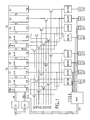
L'exemple décrit ci-après est construit à partir d'un exemple pratique simplifié dans lequel on a une mémoire de k=8 plots de sortie D0 à D7 pour extraire des mots de huit bits. La mémoire est organisée en huit groupes de colonnes, chaque groupe G0 à G7 comportant p colonnes (par exemple p=64) et correspondant à un plot respectif D0 à D7.The example described below is constructed from a simplified practical example in which there is a memory of k = 8 output pads D0 to D7 for extracting words of eight bits. The memory is organized into eight groups of columns, each group G0 to G7 comprising p columns (for example p = 64) and corresponding to a respective pad D0 to D7.
Les plots sont répartis en m=2 ensembles de r=4 plots, et dans chaque ensemble on définit une position de plot respective (1 parmi r) pour chaque plot. Les positions sont appelées p0, p1, p2, p3. Les plots D0 et D4 ont la position p0 chacun dans son ensemble, les plots D1 et D5 la position p1, etc.The pads are divided into m = 2 sets of r = 4 pads, and in each set we define a respective pad position (1 among r) for each pad. The positions are called p0, p1, p2, p3. The pads D0 and D4 have the position p0 each as a whole, the pads D1 and D5 the position p1, etc.
Les groupes sont répartis en deux ensembles Ea et Eb exactement comme les plots, puisqu'à chaque groupe correspond un plot.The groups are divided into two sets Ea and Eb exactly like the studs, since each group corresponds to a stud.
A chaque ensemble Ea et Eb est associé un groupe de colonnes de redondance respectif, CRa pour l'ensemble Ea, CRb pour l'ensemble Eb.Each set Ea and Eb is associated with a respective group of redundancy columns, CRa for the set Ea, CRb for the set Eb.
A partir de là on peut signaler que l'invention est applicable quel que soit le nombre m d'ensembles, y compris m=1, auquel cas la position de chaque plot est comprise entre 1 et k et il n'y a qu'un plot ayant une position déterminée.From there we can point out that the invention is applicable whatever the number m of sets, including m = 1, in which case the position of each pad is between 1 and k and there is only a stud having a determined position.
La mémoire comporte un décodeur de colonne DC (présent indépendamment de la redondance) pour sélectionner, lorsqu'une adresse de colonne AC est appliquée à la mémoire, une colonne parmi p dans chacun des groupes simultanément, ce qui permet l'application d'un mot de huit bits sur les sorties D0 à D7.The memory includes a DC column decoder (present independently of the redundancy) to select, when an AC column address is applied to the memory, one column among p in each of the groups simultaneously, which allows the application an eight-bit word on outputs D0 to D7.
Dans ce qui suit on parlera essentiellement de lecture même si la mémoire est inscriptible. Pour l'écriture, le mot de huit bits est appliqué aux plots D0 à D7 qui servent alors d'entrées de données et non de sorties de données.In what follows we will mainly speak of reading even if the memory is writable. For writing, the eight-bit word is applied to the pads D0 to D7 which then serve as data inputs and not data outputs.
L'adresse AC permet donc de sélectionner une colonne utile parmi p en sortie de chaque groupe.The address AC therefore makes it possible to select a useful column from among p at the output of each group.
Simultanément, cette adresse AC est appliquée à un circuit de redondance qui comporte d'abord un bloc CR1 destiné à vérifier la nécessité d'une opération de réparation de colonne et à sélectionner partiellement les colonnes de redondance servant à cette réparation.Simultaneously, this address AC is applied to a redundancy circuit which first comprises a block CR1 intended to verify the need for a column repair operation and to partially select the redundancy columns used for this repair.
Le bloc CR1 comprend d'une part des adresses de colonnes défectueuses mémorisées et d'autre part des moyens de comparaison entre les adresses reçues par la mémoire et les adresses mémorisées.The block CR1 comprises on the one hand addresses of defective columns stored and on the other hand means of comparison between the addresses received by the memory and the addresses stored.
Si on suppose qu'il y a N possibilités de réparation simultanée de colonnes défectueuses, il y a N adresses AC en mémoire. L'adresse est l'adresse d'une colonne parmi p, c'est-à-dire qu'elle ne prend pas en compte le groupe dans lequel se situe la colonne défectueuse. S'il y a 64 colonnes, les adresses AC sont des adresses de 6 bits, et le circuit CR1 comporte N groupes de 6 éléments de mémorisation qui peuvent être des transistors à grille flottante (EPROM non effaçables ou UPROM) ou des fusibles.If it is assumed that there are N possibilities of simultaneous repair of defective columns, there are N AC addresses in memory. The address is the address of a column among p, that is, it does not take into account the group in which the defective column is located. If there are 64 columns, the addresses AC are 6-bit addresses, and the circuit CR1 comprises N groups of 6 storage elements which can be floating gate transistors (non-erasable EPROMs or UPROMs) or fuses.
Le bloc CR1 reçoit les adresses AC, les compare aux N adresses défectueuses mémorisées, et fournit sur un bus de N lignes (ou 2N si on compte les signaux et leurs compléments logiques) une commande de sélection d'une colonne de redondance parmi N dans chacun des ensembles Ea, Eb, c'est-à-dire dans chacun des groupes CRa, CRb.The block CR1 receives the addresses AC, compares them to the N defective addresses stored, and provides on a bus of N lines (or 2N if the signals and their logical complements are counted) a command for selecting a redundancy column from N in each of the sets Ea, Eb, that is to say in each of the groups CRa, CRb.
Lorsqu'une adresse défectueuse est détectée, une colonne de redondance parmi N est sélectionnée en sortie de chaque groupe CRa, CRb, de même qu'une colonne normale est sélectionnée en sortie de chaque groupe G0 à G7.When a faulty address is detected, a redundancy column among N is selected at the output of each group CRa, CRb, just as a normal column is selected at the output of each group G0 to G7.
En sortie des colonnes ainsi sélectionnées, que ce soient des colonnes normales ou des colonnes de redondance, il y a un multiplexeur destiné à choisir si l'information transmise aux plots doit émaner d'une colonne normale adressée par le décodeur AC ou d'une colonne de redondance adressée par le circuit CR1, et cela individuellement pour chacun des groupes de colonnes normales et pour chacun des groupes de colonnes de redondance.At the output of the columns thus selected, whether they are normal columns or redundancy columns, there is a multiplexer intended to choose whether the information transmitted to the pads should come from a normal column addressed by the AC decoder or from a redundancy column addressed by the circuit CR1, and this individually for each of the groups of normal columns and for each of the groups of redundancy columns.
Ce multiplexeur est commandé par des signaux p0, p1, p2, p3 (et leurs compléments logiques) qui correspondent aux positions de plots des colonnes défectueuses repérées au moment du test.This multiplexer is controlled by signals p0, p1, p2, p3 (and their logical complements) which correspond to the positions of the pads of the defective columns identified at the time of the test.
Le multiplexage est le suivant : si aucune position de plot n'est sélectionnée (aucune nécessité de réparation), p0 à P3 sont tous nuls; toute transmission des colonnes de redondance aux plots ou réciproquement est interdite. La transmission entre les colonnes normales sélectionnées et les plots correspondants sont autorisées.The multiplexing is as follows: if no stud position is selected (no need for repair), p0 to P3 are all zero; any transmission of the redundancy columns to the studs or vice versa is prohibited. Transmission between the normal columns selected and the corresponding plots is authorized.
Si une réparation est nécessaire et qu'elle correspond à la position de plot p0 (p0=1, p1, p2, p3 nuls), alors la transmission depuis les groupes de colonnes normales de position p0 (G0 et G4) vers les plots de position p0 (D0 et D4) est interdite et remplacée par une transmission vers ces mêmes plots respectivement de la colonne de redondance sélectionnée par CR1 dans chacun des groupes CRa et CRb. Pour les autres positions de plot, la transmission entre les colonnes normales et les plots reste autorisée et la transmission entre les colonnes de redondance et les plots reste interdite.If a repair is necessary and it corresponds to the position of pad p0 (p0 = 1, p1, p2, p3 zero), then the transmission from the groups of normal columns of position p0 (G0 and G4) to the pads of position p0 (D0 and D4) is prohibited and replaced by a transmission to these same pads respectively of the redundancy column selected by CR1 in each of the groups CRa and CRb. For the other stud positions, transmission between the normal columns and the studs remains authorized and the transmission between the redundancy columns and the pads remains prohibited.
De même pour chacune des autres positions de plot, l'échange entre une colonne normale et une colonne de redondance ne se fait que pour la position de plot repérée par un signal logique non nul.Similarly for each of the other stud positions, the exchange between a normal column and a redundancy column is only done for the stud position identified by a non-zero logic signal.
Les signaux p0 à p3 représentant les positions de plot sont issus du bloc MPP de mémorisation de position de plot qui comprend N groupes d'éléments de mémorisation sélectionnables par le bloc CR1.The signals p0 to p3 representing the pad positions come from the pad position memorization block MPP which comprises N groups of memory elements selectable by the block CR1.
Enfin, les colonnes normales ou de redondance sélectionnées par le multiplexeur sont reliées aux plots respectifs non pas directement mais par l'intermédiaire d'un circuit de lecture/écriture respectif associé à chaque plot. Les circuits de lecture/écriture sont désignés par W0/R0 pour le premier plot, W1/R1 pour le deuxième, etc.Finally, the normal or redundancy columns selected by the multiplexer are connected to the respective pads not directly but via a respective read / write circuit associated with each pad. The read / write circuits are designated by W0 / R0 for the first pad, W1 / R1 for the second, etc.
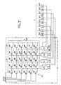
Le bloc MPP de mémorisation de position de plot est représenté en détail à la figure 2. Il est constitué sous forme d'une mémoire auxiliaire matricielle, avec des circuits de lecture et d'écriture des données stockées dans cette mémoire auxiliaire.The block MPP for storing the position of the pad is shown in detail in FIG. 2. It is constituted in the form of an auxiliary matrix memory, with circuits for reading and writing the data stored in this auxiliary memory.
La mémoire auxiliare MA comporte N lignes de cellules de mémoire électriquement programmables et r colonnes, N étant, on le rappelle, le nombre de réparations possibles et r étant le nombre de positions de plot possibles dans chacun des m ensembles (m peut être égal à 1, auquel cas r est égal au nombre total k de plots). Chaque cellule est de préférence un transistor à grille flottante de type EPROM ou UPROM; ces cellules sont inscriptibles électriquement et non effaçables.The auxiliary memory MA comprises N rows of electrically programmable memory cells and r columns, N being, as we recall, the number of possible repairs and r being the number of possible pad positions in each of the m sets (m may be equal to 1, in which case r is equal to the total number k of plots). Each cell is preferably a floating gate transistor of the EPROM or UPROM type; these cells are electrically writable and not erasable.
Le nombre total de cellules est largement supérieur à ce qui est strictement nécessaire, et cela d'autant plus que r est plus élevé. Pour r=4, le nombre de cellules est le double de ce qui est strictement nécessaire (4N au lieu de 2N); pour r=8, le rapport est encore supérieur (8N au lieu de 3N).The total number of cells is much higher than what is strictly necessary, and all the more more than r is higher. For r = 4, the number of cells is double what is strictly necessary (4N instead of 2N); for r = 8, the ratio is even higher (8N instead of 3N).
Mais grâce à cela on évite complètement des circuits de décodage encombrants.But thanks to this, bulky decoding circuits are completely avoided.
L'adressage de cette mémoire MA du bloc MPP se fait par N conducteurs de ligne, chaque ligne de cellule comprenant un conducteur de ligne reliant les grilles de commande des transistors à grille flottante de cette ligne. Les N lignes de commande proviennent d'un bus de N conducteurs issu du bloc CR1. Ce bus est disponible en sortie du circuit CR1 puisque, comme on l'a expliqué, le circuit CR1 a pour fonction de sélectionner une colonne parmi N dans les groupes de colonnes de redondance.The addressing of this memory MA of the block MPP is done by N line conductors, each cell line comprising a line conductor connecting the control gates of the floating-gate transistors of this line. The N control lines come from a bus of N conductors coming from the block CR1. This bus is available at the output of circuit CR1 since, as explained, the function of circuit CR1 is to select a column from N in the groups of redundancy columns.
Par conséquent, chaque fois que l'on sélectionne une colonne de redondance déterminée parmi N (correspondant à un numéro de réparation déterminé) on sélectionne en même temps une ligne de la mémoire du bloc MPP.Consequently, each time that a determined redundancy column is selected from among N (corresponding to a determined repair number), a row from the memory of the MPP block is simultaneously selected.
Sur les colonnes de la mémoire on lit alors un mot de r bits. Mais la programmation de la mémoire du bloc MPP est faite de telle sorte que les mots de r bits de cette mémoire ne comprennent en fait qu'un seul bit différent des autres (par exemple un bit 1 parmi r-1 bits zéro). Cela est possible du fait que la mémoire comporte r colonnes et qu'on cherche à stocker dans cette mémoire justement une position de plot parmi r.On the columns of the memory one then reads a word of r bits. However, the programming of the memory of the MPP block is done in such a way that the words of r bits of this memory in fact comprise only one single bit different from the others (for example a
Par conséquent, on va lire sur un conducteur de colonne de la mémoire MPP un bit 1, ce conducteur définissant alors la position de plot correspondant à une colonne défectueuse : à chaque conducteur de colonne de la mémoire correspond une position de plot déterminée unique et réciproquement.Consequently, a
La lecture de la mémoire (et d'ailleurs son écriture) se font d'une manière très classique pour des mémoires EPROM, à travers un circuit de lecture/écriture respectif pour chaque colonne. Les circuits de lecture/écriture sont désignés par LE0 à LE3 pour les colonnes représentant p0 à p3 respectivement.The reading of the memory (and moreover its writing) is done in a very conventional manner for EPROM memories, through a respective read / write circuit for each column. The read / write circuits are designated by LE0 to LE3 for the columns representing p0 to p3 respectively.
On peut si on le désire, comme on fait couramment dans certaines mémoires EPROM, prévoir que les circuits de lecture/écriture fonctionnent par comparaison avec une colonne de référence comportant N transistors tous programmés de la même manière (c'est-à-dire tous programmés ou tous vierges), ces transistors étant commandés par les N conducteurs de ligne de la mémoire.It is possible, if desired, as is commonly done in certain EPROM memories, to provide that the read / write circuits operate by comparison with a reference column comprising N transistors all programmed in the same way (that is to say all programmed or all blank), these transistors being controlled by the N line conductors of the memory.
Les sorties des colonnes du bloc de mémoire de position de plot définissent les r signaux p0, p1, p2, p3 (avec leurs compléments logiques) qui sont nécessaires pour la commande du multiplexeur de la mémoire principale. Aucun décodage n'est nécessaire entre les sortie des la mémoire et les entrées de commande du multiplexeur.The outputs of the columns of the pad position memory block define the r signals p0, p1, p2, p3 (with their logic complements) which are necessary for the control of the main memory multiplexer. No decoding is required between the memory outputs and the multiplexer control inputs.
Pour l'écriture des bits de cette mémoire (écriture d'un bit parmi r dans chaque ligne), on prévoit que le circuit de lecture/écriture LE0 est relié aux plot de position 0 (D0 et D4), le circuit LE1 est relié aux plots de position 1 (D1 et D5), etc. Ainsi, la programmation d'une position de plot se fait directement, sans décodage : au moment du test de la mémoire, on détecte une information erronée sur n'importe quel plot, par exemple D6. Un bit est alors placé sur ce plot pour être inscrit dans la mémoire du bloc MPP par l'intermédiaire du circuit de lecture/écriture LE2 qui est relié à ce bit. La position de plot p2 est ainsi mémorisée.For writing the bits of this memory (writing one bit among r in each line), it is provided that the read / write circuit LE0 is connected to the position pads 0 (D0 and D4), the circuit LE1 is connected to
Dans le cas où le circuit de mémoire intégrée selon l'invention est une mémoire non effaçable par ultraviolets, par exemple lorsque c'est une mémoire flash EPROM effaçable électriquement par blocs, la mémoire de position de plot du bloc MPP peut être une mémoire EPROM; elle n'a pas besoin d'être protégée contre des ultraviolets auxquels elle serait exposée si la mémoire principale était une mémoire EPROM à fenêtre d'effacement UV. Par conséquent, la mémoire du bloc MPP n'a pas besoin d'être protégée par des masques d'aluminium et surtout par des labyrinthes de protection. Ces labyrinthes sont nécessaires pour éviter une pénétration latérale de lumière ultraviolette lors de l'effacement de la mémoire EPROM, car cette pénétration effacerait les données de redondance qui doivent être conservées. La mémoire MPP serait beaucoup plus volumineuse si elle devait être munie de ces labyrinthes de protection. L'absence de fenêtre UV pour les mémoires flash EPROM permet donc de minimiser la surface de la mémoire de positions de plot, ce qui est particulièrement avantageux.In case the integrated memory circuit according to the invention is a memory that cannot be erased by ultraviolet light, for example when it is an EPROM flash memory that can be electrically erased by blocks, the pad position memory of the MPP block can be an EPROM memory; it does not need to be protected against ultraviolet to which it would be exposed if the main memory was an EPROM memory with UV erase window. Consequently, the memory of the MPP block does not need to be protected by aluminum masks and especially by protective labyrinths. These mazes are necessary to avoid lateral penetration of ultraviolet light when erasing the EPROM memory, because this penetration would erase the redundancy data which must be kept. The MPP memory would be much larger if it were to be equipped with these protective labyrinths. The absence of a UV window for EPROM flash memories therefore makes it possible to minimize the surface of the pad position memory, which is particularly advantageous.
L'invention s'applique tout particulièrement dans le cas où les positions de plot possibles sont au nombre de k, c'est-à-dire en nombre égal au nombre de plots. Pour des mémoires fournissant des mots de huit ou seize bits, on aurait donc huit ou seize positions de plot (r=8 ou r=16) et c'est pour ces mémoires que l'invention est la plus avantageuse car elle limite considérablement l'encombrement des circuits de décodage de position de plot qui étaient auparavant nécessaires.The invention applies very particularly in the case where the possible pad positions are the number of k, that is to say a number equal to the number of pads. For memories providing words of eight or sixteen bits, there would therefore be eight or sixteen positions of pad (r = 8 or r = 16) and it is for these memories that the invention is most advantageous because it considerably limits the congestion of the pad position decoding circuits which were previously necessary.
Claims (6)
- An integrated memory having column address (AG) inputs and k input/output terminals, comprising principal circuits (G0 to G7) having normal columns and redundancy circuits (GRa, GRb) having redundancy columns- the latter comprising a unit (GR1) adapted to verify the need for a column repair operation and the said unit comparing for this purpose the column addresses received and the addresses of defective normal columns stored in memory and supplying a command for selection of redundancy circuits,- the redundancy circuits also comprising elements (MPP) for storing the position of an input/output terminal corresponding to a defective normal column,
characterized in that- the elements for storing the position of the terminal are electrically programmable memory cells present in a number equal to the number N of possible repairs multiplied by the number r of possible positions of input/output terminals, arranged in an auxiliary memory of N lines and r columns, each column of this memory corresponding to a defined input/output terminal position,- the outputs of the auxiliary memory control the transmission of the data coming from a normal column or a redundancy column on the input/output terminals. - An integrated armory according to claim 1, characterized in that the data written in each line of the auxiliary memory comprises a bit different from the r-1 other bits of the same line, this bit being positioned on the column corresponding to a terminal position connected to a defective column of the integrated memory.
- A memory according to one of claims 1 or 2, characterized in that each column of the auxiliary memory comprises a column conductor connected to a read/write circuit, the read outputs of this circuit constituting the outputs of the auxiliary memory and the input/output terminals of a given position being connected to the write inputs of the read/write circuit of the auxiliary memory column corresponding to this terminal position.
- A memory according to any one of claims 1 to 3, characterized in that it comprises k groups of p principal memory columns, each group corresponding to a terminal, distributed in m sets (Ea, Eb) of r groups, with one group of redundancy columns (CRa, CRb) associated with each set, and a multiplexer directly controlled by the outputs of the auxiliary memory for determining if the data transmitted to the terminals should be derived from a normal column or from a redundancy column of the principal memory.
- A memory according to claim 4, characterized in that the multiplexer sets the following connections from column conductors of the auxiliary memory, these conductors supplying signals corresponding to positions of terminals (p0 to p3):- if the signals defined from the columns are all zero (no need for repair), all transmission from redundancy columns to terminals of the memory or conversely is inhibited; the transmissions between the columns of the principal memory selected and the corresponding terminals are enabled, and- if a repair is necessary and it corresponds to a given terminal position, for example p0 (p0 = 1, p1, p2, and p3 are zero), then transmission from the groups of normal columns of position p0 (G0 and G4) to the terminals having the position p0 (D0 and D4) is inhibited and transmission between the redundancy columns and these terminals is enabled; transmission between the other terminals and the normal columns is enabled and transmission between the other terminals and the redundancy columns is inhibited.
- A memory according to any one of claims 1 to 5, characterized in that it comprises a circuit for selecting redundancy columns adapted to select one redundancy column from among N columns in a group of redundancy columns, and in that the outputs of the said circuit directly control the matrix lines of the auxiliary memory.
Applications Claiming Priority (2)
| Application Number | Priority Date | Filing Date | Title |
|---|---|---|---|
| FR8915508 | 1989-11-24 | ||
| FR8915508A FR2655177A1 (en) | 1989-11-24 | 1989-11-24 | REDUNDANCY CIRCUIT WITH OUTPUT PLOT POSITION STORAGE. |
Publications (2)
| Publication Number | Publication Date |
|---|---|
| EP0432004A1 EP0432004A1 (en) | 1991-06-12 |
| EP0432004B1 true EP0432004B1 (en) | 1992-09-09 |
Family
ID=9387772
Family Applications (1)
| Application Number | Title | Priority Date | Filing Date |
|---|---|---|---|
| EP90403293A Expired - Lifetime EP0432004B1 (en) | 1989-11-24 | 1990-11-21 | Redundancy circuit with the memorization of the position of the output |
Country Status (4)
| Country | Link |
|---|---|
| US (1) | US5058068A (en) |
| EP (1) | EP0432004B1 (en) |
| DE (1) | DE69000302T2 (en) |
| FR (1) | FR2655177A1 (en) |
Families Citing this family (7)
| Publication number | Priority date | Publication date | Assignee | Title |
|---|---|---|---|---|
| US5388072A (en) * | 1992-04-10 | 1995-02-07 | International Business Machines Corporation | Bit line switch array for electronic computer memory |
| JP2816062B2 (en) * | 1992-10-05 | 1998-10-27 | 株式会社東芝 | Method for erasing information from memory cells |
| US5392245A (en) * | 1993-08-13 | 1995-02-21 | Micron Technology, Inc. | Redundancy elements using thin film transistors (TFTs) |
| EP0889413A3 (en) * | 1997-06-30 | 2002-03-27 | Sun Microsystems, Inc. | System and method for interconnecting personal computer in computer workstation |
| EP1453062B1 (en) * | 2003-02-27 | 2006-06-28 | STMicroelectronics S.r.l. | Built-in testing methodology in flash memory |
| CN100468314C (en) * | 2003-03-31 | 2009-03-11 | 财团法人北九州产业学术推进机构 | Programmable logic device |
| US20050159925A1 (en) * | 2004-01-15 | 2005-07-21 | Elias Gedamu | Cache testing for a processor design |
Family Cites Families (15)
| Publication number | Priority date | Publication date | Assignee | Title |
|---|---|---|---|---|
| GB1158010A (en) * | 1966-12-21 | 1969-07-09 | Ibm | Data Storage Apparatus |
| SE358755B (en) * | 1972-06-09 | 1973-08-06 | Ericsson Telefon Ab L M | |
| JPS57129297U (en) * | 1981-02-06 | 1982-08-12 | ||
| US4471472A (en) * | 1982-02-05 | 1984-09-11 | Advanced Micro Devices, Inc. | Semiconductor memory utilizing an improved redundant circuitry configuration |
| US4672240A (en) * | 1983-02-07 | 1987-06-09 | Westinghouse Electric Corp. | Programmable redundancy circuit |
| JPS6150293A (en) * | 1984-08-17 | 1986-03-12 | Fujitsu Ltd | Semiconductor memory |
| US4598388A (en) * | 1985-01-22 | 1986-07-01 | Texas Instruments Incorporated | Semiconductor memory with redundant column circuitry |
| US4819205A (en) * | 1985-03-25 | 1989-04-04 | Motorola, Inc. | Memory system having memory elements independently defined as being on-line or off-line |
| JPS61264599A (en) * | 1985-05-16 | 1986-11-22 | Fujitsu Ltd | Semiconductor memory device |
| KR950008676B1 (en) * | 1986-04-23 | 1995-08-04 | 가부시기가이샤 히다찌세이사꾸쇼 | Semiconductor memory device and error correction method thereof |
| JPS62293598A (en) * | 1986-06-12 | 1987-12-21 | Toshiba Corp | Semiconductor storage device |
| FR2611301B1 (en) * | 1987-02-24 | 1989-04-21 | Thomson Semiconducteurs | BUILT-IN MEMORY WITH REDUNDANCED DATA COLUMNS |
| US4800535A (en) * | 1987-04-28 | 1989-01-24 | Aptec Computer Systems, Inc. | Interleaved memory addressing system and method using a parity signal |
| JPH01109599A (en) * | 1987-10-22 | 1989-04-26 | Nec Corp | Writable and erasable semiconductor memory device |
| US4831285A (en) * | 1988-01-19 | 1989-05-16 | National Semiconductor Corporation | Self precharging static programmable logic array |
-
1989
- 1989-11-24 FR FR8915508A patent/FR2655177A1/en not_active Withdrawn
-
1990
- 1990-11-21 DE DE9090403293T patent/DE69000302T2/en not_active Expired - Fee Related
- 1990-11-21 EP EP90403293A patent/EP0432004B1/en not_active Expired - Lifetime
- 1990-11-21 US US07/616,634 patent/US5058068A/en not_active Expired - Lifetime
Also Published As
| Publication number | Publication date |
|---|---|
| US5058068A (en) | 1991-10-15 |
| FR2655177A1 (en) | 1991-05-31 |
| DE69000302T2 (en) | 1993-04-22 |
| DE69000302D1 (en) | 1992-10-15 |
| EP0432004A1 (en) | 1991-06-12 |
Similar Documents
| Publication | Publication Date | Title |
|---|---|---|
| EP0674264B1 (en) | Circuit for selecting redundant memory elements and FLASH EEPROM containing said circuit | |
| EP0666573B1 (en) | Non volatile flip-flop, programmed via the source, especially for memory redundancy circuit | |
| EP1434237B1 (en) | Non-volatile SRAM memory cell | |
| EP0669576B1 (en) | Memory redundancy circuit | |
| EP0645714B1 (en) | Dynamic redundancy circuit for integrated circuit memory | |
| EP0317014A1 (en) | Random access memory unit with plural test modes and computer equipped with such units | |
| EP0334763A1 (en) | Method of testing a fleeting programmable memory, and this memory | |
| EP0432004B1 (en) | Redundancy circuit with the memorization of the position of the output | |
| US5793683A (en) | Wordline and bitline redundancy with no performance penalty | |
| FR2611301A1 (en) | Integrated memory with data column redundancy | |
| EP1052572B1 (en) | Non-volatile memory device with row redundancy | |
| EP0470897B1 (en) | Integrated memory circuit with redundancy and improved addressing in test mode | |
| FR2771839A1 (en) | Non volatile programmable memory architecture | |
| EP0977120B1 (en) | Error correction in a ROM by means of redundancy | |
| FR2695493A1 (en) | Memory circuit with redundancy. | |
| EP1168179B1 (en) | Dynamic memory with spare cells | |
| EP0675441B1 (en) | Redundancy fuses matrix array for integrated memory and implementing method | |
| EP0433141B1 (en) | Redundancy circuit for memory | |
| FR2764095A1 (en) | Memory circuit with dynamic redundancy | |
| FR2635607A1 (en) | INTERNAL METHOD FOR PROGRAMMING AUTOMATIC CONTROL AND REDUNDANCY FOR MEMORY CIRCUITS AND APPARATUS FOR APPLYING THE METHOD | |
| FR2779251A1 (en) | Means for repairing defects in dynamic random access memory, DRAM, modules, where some of the cells have too low residual magnetism | |
| FR2817982A1 (en) | Shared redundancy integrated circuit memory, uses allocation circuits associated with memory banks to switch input/output lines | |
| FR2644924A1 (en) | Circuit for selecting a redundant column in an integrated memory with data column redundancy | |
| EP0059125B1 (en) | Read-only-memory with modified addressing | |
| EP0542592A1 (en) | Integrated memory circuit comprising a redundancy system |
Legal Events
| Date | Code | Title | Description |
|---|---|---|---|
| PUAI | Public reference made under article 153(3) epc to a published international application that has entered the european phase |
Free format text: ORIGINAL CODE: 0009012 |
|
| AK | Designated contracting states |
Kind code of ref document: A1 Designated state(s): DE FR GB IT |
|
| 17P | Request for examination filed |
Effective date: 19910412 |
|
| 17Q | First examination report despatched |
Effective date: 19910808 |
|
| GRAA | (expected) grant |
Free format text: ORIGINAL CODE: 0009210 |
|
| AK | Designated contracting states |
Kind code of ref document: B1 Designated state(s): DE FR GB IT |
|
| REF | Corresponds to: |
Ref document number: 69000302 Country of ref document: DE Date of ref document: 19921015 |
|
| GBT | Gb: translation of ep patent filed (gb section 77(6)(a)/1977) | ||
| ITF | It: translation for a ep patent filed |
Owner name: AVV. ANTONIO PETRUZZELL |
|
| PLBE | No opposition filed within time limit |
Free format text: ORIGINAL CODE: 0009261 |
|
| STAA | Information on the status of an ep patent application or granted ep patent |
Free format text: STATUS: NO OPPOSITION FILED WITHIN TIME LIMIT |
|
| 26N | No opposition filed | ||
| REG | Reference to a national code |
Ref country code: FR Ref legal event code: D6 |
|
| PGFP | Annual fee paid to national office [announced via postgrant information from national office to epo] |
Ref country code: DE Payment date: 20001113 Year of fee payment: 11 |
|
| REG | Reference to a national code |
Ref country code: GB Ref legal event code: IF02 |
|
| PG25 | Lapsed in a contracting state [announced via postgrant information from national office to epo] |
Ref country code: DE Free format text: LAPSE BECAUSE OF NON-PAYMENT OF DUE FEES Effective date: 20020702 |
|
| PGFP | Annual fee paid to national office [announced via postgrant information from national office to epo] |
Ref country code: FR Payment date: 20021108 Year of fee payment: 13 |
|
| PGFP | Annual fee paid to national office [announced via postgrant information from national office to epo] |
Ref country code: GB Payment date: 20021120 Year of fee payment: 13 |
|
| PG25 | Lapsed in a contracting state [announced via postgrant information from national office to epo] |
Ref country code: GB Free format text: LAPSE BECAUSE OF NON-PAYMENT OF DUE FEES Effective date: 20031121 |
|
| GBPC | Gb: european patent ceased through non-payment of renewal fee |
Effective date: 20031121 |
|
| PG25 | Lapsed in a contracting state [announced via postgrant information from national office to epo] |
Ref country code: FR Free format text: LAPSE BECAUSE OF NON-PAYMENT OF DUE FEES Effective date: 20040730 |
|
| REG | Reference to a national code |
Ref country code: FR Ref legal event code: ST |
|
| PG25 | Lapsed in a contracting state [announced via postgrant information from national office to epo] |
Ref country code: IT Free format text: LAPSE BECAUSE OF NON-PAYMENT OF DUE FEES;WARNING: LAPSES OF ITALIAN PATENTS WITH EFFECTIVE DATE BEFORE 2007 MAY HAVE OCCURRED AT ANY TIME BEFORE 2007. THE CORRECT EFFECTIVE DATE MAY BE DIFFERENT FROM THE ONE RECORDED. Effective date: 20051121 |