EP0431999B1 - Procédé de dépôt d'une composition céramique en couche mince, et produit obtenu par ce procédé - Google Patents
Procédé de dépôt d'une composition céramique en couche mince, et produit obtenu par ce procédé Download PDFInfo
- Publication number
- EP0431999B1 EP0431999B1 EP19900403248 EP90403248A EP0431999B1 EP 0431999 B1 EP0431999 B1 EP 0431999B1 EP 19900403248 EP19900403248 EP 19900403248 EP 90403248 A EP90403248 A EP 90403248A EP 0431999 B1 EP0431999 B1 EP 0431999B1
- Authority
- EP
- European Patent Office
- Prior art keywords
- ceramic composition
- depositing
- layer
- substrate
- hexamethylenetetramine
- Prior art date
- Legal status (The legal status is an assumption and is not a legal conclusion. Google has not performed a legal analysis and makes no representation as to the accuracy of the status listed.)
- Expired - Lifetime
Links
Images


Classifications
-
- H—ELECTRICITY
- H10—SEMICONDUCTOR DEVICES; ELECTRIC SOLID-STATE DEVICES NOT OTHERWISE PROVIDED FOR
- H10P—GENERIC PROCESSES OR APPARATUS FOR THE MANUFACTURE OR TREATMENT OF DEVICES COVERED BY CLASS H10
- H10P14/00—Formation of materials, e.g. in the shape of layers or pillars
- H10P14/60—Formation of materials, e.g. in the shape of layers or pillars of insulating materials
- H10P14/63—Formation of materials, e.g. in the shape of layers or pillars of insulating materials characterised by the formation processes
- H10P14/6326—Deposition processes
- H10P14/6342—Liquid deposition, e.g. spin-coating, sol-gel techniques or spray coating
-
- C—CHEMISTRY; METALLURGY
- C04—CEMENTS; CONCRETE; ARTIFICIAL STONE; CERAMICS; REFRACTORIES
- C04B—LIME, MAGNESIA; SLAG; CEMENTS; COMPOSITIONS THEREOF, e.g. MORTARS, CONCRETE OR LIKE BUILDING MATERIALS; ARTIFICIAL STONE; CERAMICS; REFRACTORIES; TREATMENT OF NATURAL STONE
- C04B41/00—After-treatment of mortars, concrete, artificial stone or ceramics; Treatment of natural stone
- C04B41/009—After-treatment of mortars, concrete, artificial stone or ceramics; Treatment of natural stone characterised by the material treated
-
- C—CHEMISTRY; METALLURGY
- C04—CEMENTS; CONCRETE; ARTIFICIAL STONE; CERAMICS; REFRACTORIES
- C04B—LIME, MAGNESIA; SLAG; CEMENTS; COMPOSITIONS THEREOF, e.g. MORTARS, CONCRETE OR LIKE BUILDING MATERIALS; ARTIFICIAL STONE; CERAMICS; REFRACTORIES; TREATMENT OF NATURAL STONE
- C04B41/00—After-treatment of mortars, concrete, artificial stone or ceramics; Treatment of natural stone
- C04B41/45—Coating or impregnating, e.g. injection in masonry, partial coating of green or fired ceramics, organic coating compositions for adhering together two concrete elements
- C04B41/52—Multiple coating or impregnating multiple coating or impregnating with the same composition or with compositions only differing in the concentration of the constituents, is classified as single coating or impregnation
-
- C—CHEMISTRY; METALLURGY
- C04—CEMENTS; CONCRETE; ARTIFICIAL STONE; CERAMICS; REFRACTORIES
- C04B—LIME, MAGNESIA; SLAG; CEMENTS; COMPOSITIONS THEREOF, e.g. MORTARS, CONCRETE OR LIKE BUILDING MATERIALS; ARTIFICIAL STONE; CERAMICS; REFRACTORIES; TREATMENT OF NATURAL STONE
- C04B41/00—After-treatment of mortars, concrete, artificial stone or ceramics; Treatment of natural stone
- C04B41/80—After-treatment of mortars, concrete, artificial stone or ceramics; Treatment of natural stone of only ceramics
- C04B41/81—Coating or impregnation
- C04B41/89—Coating or impregnation for obtaining at least two superposed coatings having different compositions
-
- C—CHEMISTRY; METALLURGY
- C23—COATING METALLIC MATERIAL; COATING MATERIAL WITH METALLIC MATERIAL; CHEMICAL SURFACE TREATMENT; DIFFUSION TREATMENT OF METALLIC MATERIAL; COATING BY VACUUM EVAPORATION, BY SPUTTERING, BY ION IMPLANTATION OR BY CHEMICAL VAPOUR DEPOSITION, IN GENERAL; INHIBITING CORROSION OF METALLIC MATERIAL OR INCRUSTATION IN GENERAL
- C23C—COATING METALLIC MATERIAL; COATING MATERIAL WITH METALLIC MATERIAL; SURFACE TREATMENT OF METALLIC MATERIAL BY DIFFUSION INTO THE SURFACE, BY CHEMICAL CONVERSION OR SUBSTITUTION; COATING BY VACUUM EVAPORATION, BY SPUTTERING, BY ION IMPLANTATION OR BY CHEMICAL VAPOUR DEPOSITION, IN GENERAL
- C23C18/00—Chemical coating by decomposition of either liquid compounds or solutions of the coating forming compounds, without leaving reaction products of surface material in the coating; Contact plating
- C23C18/02—Chemical coating by decomposition of either liquid compounds or solutions of the coating forming compounds, without leaving reaction products of surface material in the coating; Contact plating by thermal decomposition
- C23C18/12—Chemical coating by decomposition of either liquid compounds or solutions of the coating forming compounds, without leaving reaction products of surface material in the coating; Contact plating by thermal decomposition characterised by the deposition of inorganic material other than metallic material
- C23C18/1204—Chemical coating by decomposition of either liquid compounds or solutions of the coating forming compounds, without leaving reaction products of surface material in the coating; Contact plating by thermal decomposition characterised by the deposition of inorganic material other than metallic material inorganic material, e.g. non-oxide and non-metallic such as sulfides, nitrides based compounds
- C23C18/1208—Oxides, e.g. ceramics
-
- C—CHEMISTRY; METALLURGY
- C23—COATING METALLIC MATERIAL; COATING MATERIAL WITH METALLIC MATERIAL; CHEMICAL SURFACE TREATMENT; DIFFUSION TREATMENT OF METALLIC MATERIAL; COATING BY VACUUM EVAPORATION, BY SPUTTERING, BY ION IMPLANTATION OR BY CHEMICAL VAPOUR DEPOSITION, IN GENERAL; INHIBITING CORROSION OF METALLIC MATERIAL OR INCRUSTATION IN GENERAL
- C23C—COATING METALLIC MATERIAL; COATING MATERIAL WITH METALLIC MATERIAL; SURFACE TREATMENT OF METALLIC MATERIAL BY DIFFUSION INTO THE SURFACE, BY CHEMICAL CONVERSION OR SUBSTITUTION; COATING BY VACUUM EVAPORATION, BY SPUTTERING, BY ION IMPLANTATION OR BY CHEMICAL VAPOUR DEPOSITION, IN GENERAL
- C23C18/00—Chemical coating by decomposition of either liquid compounds or solutions of the coating forming compounds, without leaving reaction products of surface material in the coating; Contact plating
- C23C18/02—Chemical coating by decomposition of either liquid compounds or solutions of the coating forming compounds, without leaving reaction products of surface material in the coating; Contact plating by thermal decomposition
- C23C18/12—Chemical coating by decomposition of either liquid compounds or solutions of the coating forming compounds, without leaving reaction products of surface material in the coating; Contact plating by thermal decomposition characterised by the deposition of inorganic material other than metallic material
- C23C18/1225—Deposition of multilayers of inorganic material
-
- H—ELECTRICITY
- H10—SEMICONDUCTOR DEVICES; ELECTRIC SOLID-STATE DEVICES NOT OTHERWISE PROVIDED FOR
- H10P—GENERIC PROCESSES OR APPARATUS FOR THE MANUFACTURE OR TREATMENT OF DEVICES COVERED BY CLASS H10
- H10P14/00—Formation of materials, e.g. in the shape of layers or pillars
- H10P14/60—Formation of materials, e.g. in the shape of layers or pillars of insulating materials
- H10P14/66—Formation of materials, e.g. in the shape of layers or pillars of insulating materials characterised by the type of materials
- H10P14/668—Formation of materials, e.g. in the shape of layers or pillars of insulating materials characterised by the type of materials the materials being characterised by the deposition precursor materials
-
- H—ELECTRICITY
- H10—SEMICONDUCTOR DEVICES; ELECTRIC SOLID-STATE DEVICES NOT OTHERWISE PROVIDED FOR
- H10P—GENERIC PROCESSES OR APPARATUS FOR THE MANUFACTURE OR TREATMENT OF DEVICES COVERED BY CLASS H10
- H10P14/00—Formation of materials, e.g. in the shape of layers or pillars
- H10P14/60—Formation of materials, e.g. in the shape of layers or pillars of insulating materials
- H10P14/69—Inorganic materials
- H10P14/692—Inorganic materials composed of oxides, glassy oxides or oxide-based glasses
- H10P14/6938—Inorganic materials composed of oxides, glassy oxides or oxide-based glasses the material containing at least one metal element, e.g. metal oxides, metal oxynitrides or metal oxycarbides
- H10P14/6939—Inorganic materials composed of oxides, glassy oxides or oxide-based glasses the material containing at least one metal element, e.g. metal oxides, metal oxynitrides or metal oxycarbides characterised by the metal
- H10P14/69397—Inorganic materials composed of oxides, glassy oxides or oxide-based glasses the material containing at least one metal element, e.g. metal oxides, metal oxynitrides or metal oxycarbides characterised by the metal the material containing two or more metal elements
-
- H—ELECTRICITY
- H10—SEMICONDUCTOR DEVICES; ELECTRIC SOLID-STATE DEVICES NOT OTHERWISE PROVIDED FOR
- H10P—GENERIC PROCESSES OR APPARATUS FOR THE MANUFACTURE OR TREATMENT OF DEVICES COVERED BY CLASS H10
- H10P72/00—Handling or holding of wafers, substrates or devices during manufacture or treatment thereof
- H10P72/04—Apparatus for manufacture or treatment
- H10P72/0431—Apparatus for thermal treatment
-
- H—ELECTRICITY
- H10—SEMICONDUCTOR DEVICES; ELECTRIC SOLID-STATE DEVICES NOT OTHERWISE PROVIDED FOR
- H10P—GENERIC PROCESSES OR APPARATUS FOR THE MANUFACTURE OR TREATMENT OF DEVICES COVERED BY CLASS H10
- H10P14/00—Formation of materials, e.g. in the shape of layers or pillars
- H10P14/60—Formation of materials, e.g. in the shape of layers or pillars of insulating materials
- H10P14/69—Inorganic materials
- H10P14/692—Inorganic materials composed of oxides, glassy oxides or oxide-based glasses
- H10P14/6938—Inorganic materials composed of oxides, glassy oxides or oxide-based glasses the material containing at least one metal element, e.g. metal oxides, metal oxynitrides or metal oxycarbides
- H10P14/69398—Inorganic materials composed of oxides, glassy oxides or oxide-based glasses the material containing at least one metal element, e.g. metal oxides, metal oxynitrides or metal oxycarbides the material having a perovskite structure, e.g. BaTiO3
-
- Y—GENERAL TAGGING OF NEW TECHNOLOGICAL DEVELOPMENTS; GENERAL TAGGING OF CROSS-SECTIONAL TECHNOLOGIES SPANNING OVER SEVERAL SECTIONS OF THE IPC; TECHNICAL SUBJECTS COVERED BY FORMER USPC CROSS-REFERENCE ART COLLECTIONS [XRACs] AND DIGESTS
- Y10—TECHNICAL SUBJECTS COVERED BY FORMER USPC
- Y10T—TECHNICAL SUBJECTS COVERED BY FORMER US CLASSIFICATION
- Y10T428/00—Stock material or miscellaneous articles
- Y10T428/31504—Composite [nonstructural laminate]
- Y10T428/31678—Of metal
Definitions
- the invention relates to a process for depositing a ceramic composition in a thin layer and the product obtained by this process. It was designed in collaboration between the Ceramics laboratory of the Central Research Laboratory of THOMSON-CSF on the one hand and the Physics of Condensed Matter laboratory of the University of PARIS VI (CNRS) directed by Pr. Jacques LIVAGE d 'somewhere else.
- oxide ceramics have potential applications in the field of microelectronics. These are for example perovskites with dielectric applications such as PbTi x Zr 1-x O3 ferroelectrics or materials with conductive and transparent properties such as In x Sn 1-x O oxides or superconductors based copper and oxides of elements such as (Y, Ba), (Bi, Sr, Ca) or (Ti, Ba, Ca).
- These compounds must be deposited in a thin layer on substrates such as alumina, silicon or silica SiO2 on which may have previously been deposited buffer layers such as other oxides or noble metals whose purpose is either to serve as an electrical contact (or as an insulator) or to ensure better adhesion of the ceramic film to the substrate.
- substrates such as alumina, silicon or silica SiO2 on which may have previously been deposited buffer layers such as other oxides or noble metals whose purpose is either to serve as an electrical contact (or as an insulator) or to ensure better adhesion of the ceramic film to the substrate.
- a common technique for depositing ceramic films is screen printing where the oxide powders, previously reacted, are mixed with a binder and applied to the substrate. It is then a question of heating to eliminate the organic binder and to obtain a sintering of the powder grains between them which will ensure a better density of the ceramic, better properties. electronic and possibly optical properties such as transparency.
- the need for integration in increasingly reduced systems requires submicron starting powders to obtain low roughness. This is however difficult to obtain by conventional methods of synthesis based on a mixture of dry powders.
- the possible anisotropy of the properties linked to an anisotropy of the crystal structure of the material itself may require texturing of the ceramic by aligning the grains parallel to the substrate. This can be achieved by direct crystallization of the phases oriented by the substrate.
- the crystallization of the desired phase as well as its densification is done conventionally at temperatures close to the melting temperature of the materials in order to ensure easy mobility of the cations.
- this will also cause reactions with the latter or with other layers in the case of multilayer processes.
- the difference in expansion coefficients of the different elements will cause crazing at high temperatures. It is therefore necessary to find methods which favor a low synthesis temperature. Another reason may be the volatility of certain elements (Pb, Bi) at high temperature.
- alkoxides sol-gel processes. Their hydrolysis leads to the condensation of polymer networks of oxides and hydroxides precursors of the desired phases. However, it is sometimes difficult to control the rate of hydrolysis when it comes to the synthesis of complex phases containing a large number of elements with different properties. It is difficult to control both the chemical homogeneity which will allow the lowering of the synthesis temperature and the rheology desirable for the deposition. On the other hand, the handling of alkoxides is not always easy.
- the present invention relates to a method of depositing a ceramic composition in a thin layer from a homogeneous solution, the rheology of which can be adapted to deposit with a spinner (also called “wafer spinning" in the Anglo-Saxon terminology) of multicomponent systems.
- the cations are dissolved in a solution where polymerization (or maturation) is caused by the reaction of 2 organic compounds: acetylacetone (ACAC) and hexamethylenetetramine (HMTA).
- the two compounds (ACAC and HMTA) used by the process according to the invention are preferably added in the optimal molar ratio of 2 moles of ACAC for 1 mole of HMTA.
- these compounds react to give a polymeric species. Since, moreover, they form very good complexing agents (in particular acetylacetone) independently of the nature of the cations, they keep these cations solubilized in the polymeric medium when it is formed and during drying on the deposition substrate.
- the method according to the invention has a double advantage. First of all, it allows easy adaptation to a large number of different systems and it is therefore possible to combine in solution in the same synthesis elements whose chemical behavior is very different. It then allows an easy adaptation of the rheology. Once the synthesis has been obtained, a polymer is formed which chelates the cations and whose concentration determines the viscosity. The substance obtained is viscous and wetting. It is then possible by simple elimination of the solvent to modify it. It does not change over time and this allows the storage of deposition solution and a rigorous control of its adaptation to the chosen deposition mode.
- the substance obtained can be used as it is for spinning deposition (deposit conditions: 20 seconds, 2000 revolutions per minute) on substrates such as corundum and silicon previously coated with platinum (by vacuum deposition) to ensure good electrical conduction.
- Drying can be done at 300 ° C in an oven.
- the layer is sintered at a temperature of around 700-750 ° C, which does not alter the substrate on which the layer is deposited.
- thermogravimetric and differential calorimetry analysis carried out on the lead titanate thus deposited shows that an advantage of the method is the smooth and regular loss of mass of the substance when its temperature increases.
- acetic acid propanol or methoxyethanol
- solvent Besides acetic acid, propanol or methoxyethanol can be used as solvent.
- FIG. 1 represents a diagram giving, as a function of the temperature, the mass loss curve (curve 1 corresponding to the ordinate axis on the left) and its derived curve (curve 2 corresponding to the ordinate axis on the right) . It is found that indeed the loss of mass is gentle and regular with temperature. This shows an advantage of the method which is not to cause an excessively violent oxidation of the organic part which would cause the film to be earthen. Exothermic phenomena end at 700 ° C, the temperature at which the phase is crystallized.
- the thickness of the layers obtained can vary between 0.2 and 5 ⁇ m per layer. Thicker deposits are therefore obtained directly than by known sol-gel methods, but very thin deposits can also be obtained due to the excellent surface condition of the layer.
- FIG. 3 is a diagram showing the capacity C as a function of the voltage V. It is noted that the capacity-voltage curve is asymmetrical for increasing and decreasing voltages between -20 volts and + 20 volts. The decreasing normal curve of the MIS structure is superimposed on peaks towards + or - 6 volts due to the tilting of the ferroelectric domains.
- the invention makes it possible to create thin layers of large areas, without defects, of thickness less than one micron on different metallic (or metallized), semiconductor or insulating substrates with a simple, inexpensive process, requiring common raw materials. and cheap.
- Applications are in the field of non-volatile memories, integrated optics, superconducting devices, acoustic or pyroelectric detectors.
- the deposits according to the invention have a very low surface roughness and a very good surface condition due to the fineness and the homogeneity of the grains of the ceramic.
Landscapes
- Chemical & Material Sciences (AREA)
- Engineering & Computer Science (AREA)
- Ceramic Engineering (AREA)
- Materials Engineering (AREA)
- Organic Chemistry (AREA)
- Structural Engineering (AREA)
- Inorganic Chemistry (AREA)
- Physics & Mathematics (AREA)
- Thermal Sciences (AREA)
- General Chemical & Material Sciences (AREA)
- Chemical Kinetics & Catalysis (AREA)
- Mechanical Engineering (AREA)
- Metallurgy (AREA)
- Compositions Of Oxide Ceramics (AREA)
- Inorganic Insulating Materials (AREA)
Description
- L'invention concerne un procédé de dépôt d'une composition céramique en couche mince et le produit obtenu par ce procédé. Elle a été conçue en collaboration entre le laboratoire Céramiques du Laboratoire Central de Recherches de THOMSON-CSF d'une part et le laboratoire de Physique de la Matière Condensée de l'Université de PARIS VI (CNRS) dirigé par le Pr. Jacques LIVAGE d'autre part.
- Un grand nombre de céramique d'oxydes ont des applications potentielles dans le domaine de la microélectronique. Il s'agit par exemple de pérovskites à applications diélectriques telles que les ferroélectriques PbTixZr1-xO₃ ou bien des matériaux à propriétés conductrices et transparentes tels que les oxydes d'InxSn1-xO ou encore des supraconducteurs à base de cuivre et d'oxydes d'éléments tels que (Y, Ba), (Bi, Sr, Ca) ou (Ti, Ba, Ca).
- Ces composés doivent être déposés en couche mince sur des substrats tels que l'alumine, le silicium ou la silice SiO₂ sur lesquels peuvent avoir été préalablement déposées des couches tampons telles que d'autres d'oxydes ou des métaux nobles dont le but est soit de servir de contact électrique (ou d'isolant) soit d'assurer une meilleure adhérence du film céramique sur le substrat.
- Une technique courante de dépôt de films céramiques est la sérigraphie où les poudres d'oxydes, préalablement réagies, sont mélangées à un liant et appliquées sur le substrat. Il s'agit alors de chauffer pour éliminer le liant organique et obtenir un frittage des grains de poudre entre eux qui assurera une meilleure densité de la céramique, des meilleures propriétés électroniques et éventuellement des propriétés optiques telles que la transparence.
- La reproductibilité et la fiabilité des propriétés de films ainsi déposés sont liées à leur microstructure et au traitement thermique imposés aux films.
- La nécessité d'intégration dans des systèmes de plus en plus réduits impose des poudres de départ submicroniques pour obtenir une faible rugosité. Ceci est cependant difficilement obtenu par les méthodes de synthèse classique à base de mélange de poudres sèches. De plus, l'anisotropie éventuelle des propriétés liée A une anisotropie de la structure cristalline du matériau lui-même peut requérir une texturation de la céramique en alignant les grains parallèlement au substrat. Ceci peut être réalisé par la cristallisation directe des phases orientées par le substrat.
- La cristallisation de la phase souhaitée ainsi que sa densification se font de façon conventionnelle à des températures proches de la température de fusion des matériaux afin d'assurer une mobilité aisée des cations. Malheureusement, dans le cas de dépôt sur un substrat cela provoquera également des réactions avec celui-ci ou avec d'autres couches dans le cas de procédés multicouches. De plus, la différence de coefficients de dilatation des différents éléments provoquera du faïençage à haute température. Il est donc nécessaire de trouver des procédés favorisant une température de synthèse basse. Une autre raison peut être la volatilité de certains éléments (Pb, Bi) à haute température.
- Une possibilité de faible coût pour le dépôt de films est la synthèse à partir de solutions où le mélange homogène des éléments permet de s'affranchir du problème de la barrière de diffusion ionique et d'abaisser ainsi la température de synthèse. La difficulté est alors d'obtenir des solutions dont les propriétés rhéologiques permettent un dépôt de films homogènes avant le traitement thermique.
- Des précurseurs intéressants de ces synthèses en solution sont les alkoxydes (procédés sol-gel). Leur hydrolyse mène à la condensation de réseaux polymériques d'oxydes et d'hydroxydes précurseurs des phases souhaitées. Néanmoins, il est parfois peu évident de contrôler le taux d'hydrolyse lorsqu'il s'agit de la synthèse de phases complexes contenant un grand nombre d'éléments aux propriétés différentes. On peut difficilement contrôler à la fois l'homogénéité chimique qui permettra l'abaissement de la température de synthèse et la rhéologie souhaitable pour le dépôt. D'autre part, la manipulation des alkoxydes n'est pas toujours aisée.
- On peut alors partir de solutions ioniques dont la viscosité et l'élasticité ont été modifiées par la présence d'agents modificateurs ajoutés aux solvants (glycol, glycérol, acide citrique) tels que des poly-alcools, des poly-acides conduisant à des résines polymères. Cependant, tous ces additifs ne sont pas forcément compatibles avec les cations. Il faut également une solution qui adhère bien au substrat pendant le dépôt. C'est un procédé compliqué et la substance obtenue se dépose très difficilement par la méthode dite "à la tournette".
- Afin de pallier ces inconvénients, la présente invention porte sur un procédé de dépôt d'une composition céramique en couche mince à partir d'une solution homogène dont la rhéologie peut être adaptée au dépôt à la tournette (encore appelé "wafer spinning" dans la terminologie anglo-saxonne) de systèmes multicomposants. Les cations sont solubilisés dans une solution où une polymérisation (ou maturation) est provoquée par la réaction de 2 composés organiques : l'acétylacétone (ACAC) et l'hexaméthylènetétramine (HMTA).
- L'invention a donc pour objet un procédé de dépôt d'une composition céramique en couche mince sur un substrat, caractérisé en ce qu'il comporte les étapes suivantes :
- dissolution des constituants de base de la composition céramique, introduits sous forme simple ou complexée, dans un solvant,
- ajout à la solution obtenue précédemment d'acétylacétone et d'hexaméthylènetétramine dans des proportions appropriées à la méthode de dépôt choisie,
- maturation ou polymérisation de la substance obtenue à l'étape précédente,
- dépôt sous forme de couche de la substance sur le substrat,
- éventuellement séchage de la couche déposée si plusieurs dépôts sont nécessaires,
- frittage à une température d'environ 700-750°C de la couche ou des couches déposées.
- L'invention sera mieux comprise et d'autres avantages apparaîtront à la lecture de la description qui va suivre, donnée à titre non limitatif, et grâce aux dessins annexés parmi lesquels :
- la figure 1 représente un diagramme donnant la perte de masse d'une substance selon l'invention, ainsi que sa dérivée, en fonction de la température,
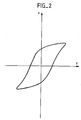
- la figure 2 représente un cycle d'hystérésis,
- la figure 3 est un diagramme montrant la variation de capacité d'une composition céramique déposée sur silicium selon l'invention en fonction de la tension.
- Les deux composés (ACAC et HMTA) utilisés par le procédé selon l'invention sont ajoutés de préférence dans le rapport molaire optimal de 2 moles d'ACAC pour 1 mole de HMTA. En milieu acide ces composés réagissent pour donner une espèce polymérique. Comme de plus ils forment de très bons agents complexants (en particulier l'acétylacétone) indépendamment de la nature des cations, ils maintiennent ces cations solubilisés dans le milieu polymérique quand il se forme et pendant le séchage sur le substrat de dépôt.
- Le procédé selon l'invention présente un double intérêt. Il permet d'abord une adaptation aisée à un grand nombre de systèmes différents et on peut donc associer en solution dans une même synthèse des éléments dont le comportement chimique est très différent. Il permet ensuite une adaptation aisée de la rhéologie. Une fois la synthèse obtenue, un polymère est formé qui chélate les cations et dont la concentration détermine la viscosité. La substance obtenue est visqueuse et mouillante. On peut alors par simple élimination du solvant modifier celle-ci. Elle n'évolue pas au cours du temps et ceci permet le stockage de solution de dépôt et un contrôle rigoureux de son adaptation au mode de dépôt choisi.
- A titre d'exemple, on va décrire maintenant la synthèse du titanate de plomb PbTiO₃.
- On dissout dans 50 ml d'acide acétique 8,5 g de tétrabutoxyde de titane Ti (OBut)₄ et 9,2 g d'acétate de plomb. On ajoute ensuite 10 ml d'acétylacétone et 4 g d'hexaméthylènetétramine. La solution jaune au départ rougit et devient visqueuse pour arriver à un régime stable au bout de quelques heures. Sa viscosité peut alors être ajustée en évaporant l'acide acétique.
- La substance obtenue peut être utilisée telle qu'elle pour un dépôt à la tournette (conditions de dépôt : 20 secondes, 2000 tours à la minute) sur des substrats tels que le corindon et le silicium préalablement recouverts de platine (par dépôt sous vide) pour assurer une bonne conduction électrique.
- Selon l'épaisseur de la couche totale à déposer il peut être nécessaire d'effectuer le dépôt en plusieurs fois et donc de sécher chaque couche déposée avant d'en déposer une nouvelle. Le séchage peut se faire à 300°C dans une étuve.
- Une fois obtenue l'épaisseur de couche désirée, la couche est frittée à une température d'environ 700-750°C, ce qui n'altère pas le substrat sur lequel la couche est déposée.
- Une analyse thermogravimétrique et de calorimétrie différentielle effectuée sur le titanate de plomb ainsi déposé montre qu'un intérêt de la méthode est la douce et régulière perte de masse de la substance lorsque sa température augmente.
- Outre l'acide acétique, on peut utiliser comme solvant le propanol ou le méthoxyéthanol.
- La figure 1 représente un diagramme donnant, en fonction de la température, la courbe de perte de masse (courbe 1 correspondant à l'axe des ordonnées de gauche) et sa courbe dérivée (courbe 2 correspondant à l'axe des ordonnées de droite). On constate qu'effectivement la perte de masse est douce et régulière avec la température. Ceci montre un intérêt de la méthode qui est de ne pas provoquer une oxydation trop violente de la partie organique qui provoquerait un faïencage du film. Les phénomènes exothermiques s'achèvent à 700°C, température à laquelle la phase est cristallisée.
- L'épaisseur des couches obtenues peut varier entre 0,2 et 5 µm par couche. On obtient donc directement des dépôts plus épais que par les méthodes sol-gel connues mais on peut aussi obtenir des dépôts très minces en raison de l'excellent état de surface de la couche.
- Les caractéristiques électriques des couches déposées sur platine (électrode déposée par pulvérisation cathodique sur un substrat de silicium orienté 100) et directement sur silicium dopé (de résistivité inférieure à 0,01 Ω . cm) sont données dans le tableau 1 placé en fin de description. Les mesures électriques sont réalisées sur des plots de métallisation en argent déposés sur la surface de la couche et de surface 7mm². Dans ce tableau, on a mentionné la capacité C mesurée, les pertes tgδ, la résistance d'isolement Ri, la tension de claquage VC en volts (pour une couche de céramique d'épaisseur d'environ 1 µm), la tension correspondant au champ coercitif Vcoerc et la rémanence R de la polarisation (pour la structure métal-isolant-métal sur platine) et de la capacité (pour la structure métal-isolant-semiconducteur sur silicium).
- Sur le platine, en raison de la faible valeur des pertes diélectriques (3 % ), de la forte valeur de la résistance d'isolement (100 MΩ) et de la tension de claquage (40 V), on a pu réaliser des cycles d'hystérésis à 60 Hz par la méthode de Sawyer et Tower. L'un de ces cycles est représenté à la figure 2 où l'axe des ordonnées représente la polarisation P et l'axe des abscisses le champ électrique E appliqué. La tension coercitive est au plus égale à 16 V et la polarisation rémanente est au moins égale à 4,3 µC/cm².
- Sur le silicium dopé, la valeur de la capacité est un peu plus faible, probablement en raison d'une capacité série causée dans le semiconducteur par des états d'interface. Sur cette structure métal-isolant-semiconducteur (MIS) on a pu cependant observer un effet de mémoire de la capacité. La figure 3 est un diagramme montrant la capacité C en fonction de la tension V. On remarque que la courbe capacité-tension est dissymétrique pour des tensions croissantes et décroissantes entre -20 volts et + 20 volts. A la courbe normale décroissante de la structure MIS se superpose des pics vers + ou - 6 volts dus au basculement des domaines ferroélectriques.
- En résumé, l'invention permet de créer des couches minces de grandes surfaces, sans défaut, d'épaisseur inférieure au micron sur différents substrats métalliques (ou métallisés), semiconducteurs ou isolants avec un procédé simple, peu coûteux, nécessitant des matières premières courantes et bon marché. Les applications se situent dans le domaine des mémoires non volatiles, de l'optique intégrée, des dispositifs à supraconducteurs, des détecteurs acoustiques ou pyroélectriques.
- Les dépôts selon l'invention présentent une très faible rugosité de surface et un très bon état de surface dû à la finesse et à l'homogénéité des grains de la céramique.

Claims (4)
- Procédé de dépôt d'une composition céramique en couche mince sur un substrat, caractérisé en ce qu'il comporte les étapes suivantes :- dissolution des constituants de base de la composition céramique, introduits sous forme simple ou complexée, dans un solvant,- ajout à la solution obtenue précédemment d'acétylacétone et d'hexaméthylènetétramine dans des proportions appropriées à la méthode de dépôt choisie,- maturation ou polymérisation de la substance obtenue à l'étape précédente,- dépôt sous forme de couche de la substance sur le substrat,- éventuellement séchage de la couche déposée si plusieurs dépôts sont nécessaires,- frittage à une température d'environ 700-750°C de la couche ou des couches déposées.
- Procédé de dépôt selon la revendication 1, caractérisé en ce que les proportions d'acétylacétone et d'hexaméthylènetétramine sont de 2 moles d'acétylacétone pour 1 mole d'hexaméthylènetétramine.
- Procédé de dépôt selon l'une des revendications 1 ou 2, caractérisé en ce que le solvant est de l'acide acétique, du propanol ou du méthoxyéthanol.
- Procédé selon l'une des revendications 1 ou 2, caractérisé en ce que la composition céramique étant du titanate de plomb, le titane est introduit sous forme de tétrabutoxyde de titane et le plomb sous forme d'acétate de plomb, le solvant étant de l'acide acétique.
Applications Claiming Priority (2)
| Application Number | Priority Date | Filing Date | Title |
|---|---|---|---|
| FR8915174 | 1989-11-20 | ||
| FR8915174A FR2654720B1 (fr) | 1989-11-20 | 1989-11-20 | Procede de depot d'une composition ceramique en couche mince et produit obtenu par ce procede. |
Publications (2)
| Publication Number | Publication Date |
|---|---|
| EP0431999A1 EP0431999A1 (fr) | 1991-06-12 |
| EP0431999B1 true EP0431999B1 (fr) | 1994-03-30 |
Family
ID=9387545
Family Applications (1)
| Application Number | Title | Priority Date | Filing Date |
|---|---|---|---|
| EP19900403248 Expired - Lifetime EP0431999B1 (fr) | 1989-11-20 | 1990-11-16 | Procédé de dépôt d'une composition céramique en couche mince, et produit obtenu par ce procédé |
Country Status (4)
| Country | Link |
|---|---|
| US (1) | US5244691A (fr) |
| EP (1) | EP0431999B1 (fr) |
| DE (1) | DE69007757T2 (fr) |
| FR (1) | FR2654720B1 (fr) |
Families Citing this family (12)
| Publication number | Priority date | Publication date | Assignee | Title |
|---|---|---|---|---|
| US5612082A (en) * | 1991-12-13 | 1997-03-18 | Symetrix Corporation | Process for making metal oxides |
| US5271955A (en) * | 1992-04-06 | 1993-12-21 | Motorola, Inc. | Method for making a semiconductor device having an anhydrous ferroelectric thin film |
| GB9224242D0 (en) * | 1992-11-19 | 1993-01-06 | Rank Brimar Ltd | Preparation of metal or oxide films |
| JPH06305713A (ja) * | 1993-04-16 | 1994-11-01 | Texas Instr Japan Ltd | ゾルーゲル法による強誘電体膜の形成方法及びキャパシタの製造方法、及びその原料溶液 |
| US6591634B1 (en) * | 1994-02-25 | 2003-07-15 | Toshinori Morizane | Method for production of metal oxide glass film at a low temperature |
| JP3252609B2 (ja) * | 1994-07-19 | 2002-02-04 | 株式会社村田製作所 | セラミック原料粉体の製造方法 |
| US6063714A (en) * | 1995-11-16 | 2000-05-16 | Texas Instruments Incorporated | Nanoporous dielectric thin film surface modification |
| DE19609942C1 (de) * | 1996-03-14 | 1997-10-30 | Heraeus Gmbh W C | Lüsterfarbe für die Dekoration von Glas, Keramik und Porzelan |
| DE19743270A1 (de) * | 1997-09-30 | 1999-04-01 | Siemens Ag | Herstellverfahren für eine keramische Schicht |
| US6641939B1 (en) | 1998-07-01 | 2003-11-04 | The Morgan Crucible Company Plc | Transition metal oxide doped alumina and methods of making and using |
| FR2811317B1 (fr) * | 2000-07-07 | 2002-10-11 | Thomson Csf | Resine reticulee et procede de fabrication d'oxydes utilisant cette resine reticulee |
| US20070098905A1 (en) * | 2004-06-17 | 2007-05-03 | Electricite De France Service National | Method for preparing metal oxide layers |
Family Cites Families (7)
| Publication number | Priority date | Publication date | Assignee | Title |
|---|---|---|---|---|
| US4481134A (en) * | 1982-01-29 | 1984-11-06 | The United States Of America As Represented By The United States Department Of Energy | Method for forming microspheres for encapsulation of nuclear waste |
| US4485094A (en) * | 1983-01-28 | 1984-11-27 | Westinghouse Electric Corp. | Method of making ABO3 of the cubic perovskite structure |
| US4960618A (en) * | 1987-01-07 | 1990-10-02 | Tokyo Ohka Kogyo Co., Ltd. | Process for formation of metal oxide film |
| US4946710A (en) * | 1987-06-02 | 1990-08-07 | National Semiconductor Corporation | Method for preparing PLZT, PZT and PLT sol-gels and fabricating ferroelectric thin films |
| ATE73739T1 (de) * | 1987-07-02 | 1992-04-15 | Mitsui Petrochemical Ind | Verfahren zur herstellung von bariumtitanaten. |
| DE3873512T2 (de) * | 1988-02-19 | 1992-12-03 | Tohru Yamamoto | Katalysator fuer das ein metallalkoxid verwendendes sol-gel-verfahren und das oxid verwendende sol-gel-verfahren. |
| US4913708A (en) * | 1988-11-18 | 1990-04-03 | Norton Company | Grinding wheel |
-
1989
- 1989-11-20 FR FR8915174A patent/FR2654720B1/fr not_active Expired - Lifetime
-
1990
- 1990-11-16 DE DE69007757T patent/DE69007757T2/de not_active Expired - Fee Related
- 1990-11-16 EP EP19900403248 patent/EP0431999B1/fr not_active Expired - Lifetime
- 1990-11-20 US US07/616,081 patent/US5244691A/en not_active Expired - Fee Related
Also Published As
| Publication number | Publication date |
|---|---|
| EP0431999A1 (fr) | 1991-06-12 |
| FR2654720B1 (fr) | 1992-01-31 |
| US5244691A (en) | 1993-09-14 |
| FR2654720A1 (fr) | 1991-05-24 |
| DE69007757D1 (de) | 1994-05-05 |
| DE69007757T2 (de) | 1994-07-28 |
Similar Documents
| Publication | Publication Date | Title |
|---|---|---|
| US4946710A (en) | Method for preparing PLZT, PZT and PLT sol-gels and fabricating ferroelectric thin films | |
| Xu et al. | Ferroelectric thin films prepared by sol-gel processing | |
| US5614018A (en) | Integrated circuit capacitors and process for making the same | |
| US5358889A (en) | Formation of ruthenium oxide for integrated circuits | |
| Haertling | PLZT thin films prepared from acetate precursors | |
| JP3476932B2 (ja) | 強誘電体薄膜及び強誘電体薄膜被覆基板並びに強誘電体薄膜の製造方法 | |
| EP0431999A1 (fr) | Procédé de dépôt d'une composition céramique en couche mince, et produit obtenu par ce procédé | |
| JPH08239264A (ja) | ホウ素を用いたチタン酸バリウム・ストロンチウム薄膜 | |
| JPH04230011A (ja) | 単一層コンデンサーの製造方法 | |
| WO1990013149A1 (fr) | PROCEDE SOL-GEL DE PREPARATION DE MINCES FILMS EN Pb(Zr,Ti)O¿3? | |
| US5723361A (en) | Thin films of ABO3 with excess A-site and B-site modifiers and method of fabricating integrated circuits with same | |
| US6528863B1 (en) | Perovskite-containing composite material, method of manufacturing said material, electronic component and module | |
| JP4122430B2 (ja) | 強誘電体膜 | |
| US6025619A (en) | Thin films of ABO3 with excess A-site and B-site modifiers and method of fabricating integrated circuits with same | |
| Xu et al. | Antiferroelectric thin and thick films for high-strain microactuators | |
| FR2829757A1 (fr) | Procede de preparation d'un sol stable de zircono-titanate de plomb et procede de preparation de films a partir dudit sol | |
| WO2002031873A1 (fr) | Incorporation de nitrure de titane et de nitrure de tantale dans de l'oxyde de tantale cvd pour former des condensateurs mim | |
| Gaskey et al. | “Square” hysteresis loops in phase-switching Nb-doped lead zirconate stannate titanate thin films | |
| EP1846344B1 (fr) | Procede de preparation de ceramiques oxydes a base de plomb, de titane, de zirconium et de lanthanide(s) | |
| JPH08111411A (ja) | 強誘電体薄膜の製造方法 | |
| Adem | Preparation of BaxSr1-xTiO3 thin films by chemical solution deposition and their electrical characterization | |
| KR100345014B1 (ko) | 갈륨비소 기판의 박막 커패시터와 그 제조 방법 | |
| KR100252744B1 (ko) | 과잉의 A사이트와 B사이트 개질제(modifier)를 가진 ABO₃의 박막 및 그 박막을 가진 집적회로의 제조방법 | |
| US6007868A (en) | Method of manufacturing ferroelectric bismuth-titanate layers on a substrate from solution | |
| JPH0624222B2 (ja) | 薄膜コンデンサの製造方法 |
Legal Events
| Date | Code | Title | Description |
|---|---|---|---|
| PUAI | Public reference made under article 153(3) epc to a published international application that has entered the european phase |
Free format text: ORIGINAL CODE: 0009012 |
|
| AK | Designated contracting states |
Kind code of ref document: A1 Designated state(s): DE GB |
|
| 17P | Request for examination filed |
Effective date: 19911130 |
|
| 17Q | First examination report despatched |
Effective date: 19930430 |
|
| RAP1 | Party data changed (applicant data changed or rights of an application transferred) |
Owner name: THOMSON-CSF |
|
| GRAA | (expected) grant |
Free format text: ORIGINAL CODE: 0009210 |
|
| AK | Designated contracting states |
Kind code of ref document: B1 Designated state(s): DE GB |
|
| REF | Corresponds to: |
Ref document number: 69007757 Country of ref document: DE Date of ref document: 19940505 |
|
| GBT | Gb: translation of ep patent filed (gb section 77(6)(a)/1977) |
Effective date: 19940511 |
|
| PLBE | No opposition filed within time limit |
Free format text: ORIGINAL CODE: 0009261 |
|
| STAA | Information on the status of an ep patent application or granted ep patent |
Free format text: STATUS: NO OPPOSITION FILED WITHIN TIME LIMIT |
|
| 26N | No opposition filed | ||
| REG | Reference to a national code |
Ref country code: GB Ref legal event code: IF02 |
|
| PGFP | Annual fee paid to national office [announced via postgrant information from national office to epo] |
Ref country code: GB Payment date: 20031112 Year of fee payment: 14 |
|
| PGFP | Annual fee paid to national office [announced via postgrant information from national office to epo] |
Ref country code: DE Payment date: 20031127 Year of fee payment: 14 |
|
| PG25 | Lapsed in a contracting state [announced via postgrant information from national office to epo] |
Ref country code: GB Free format text: LAPSE BECAUSE OF NON-PAYMENT OF DUE FEES Effective date: 20041116 |
|
| PG25 | Lapsed in a contracting state [announced via postgrant information from national office to epo] |
Ref country code: DE Free format text: LAPSE BECAUSE OF NON-PAYMENT OF DUE FEES Effective date: 20050601 |
|
| GBPC | Gb: european patent ceased through non-payment of renewal fee |
Effective date: 20041116 |