EP0430516A2 - A periodic array with a nearly ideal element pattern - Google Patents
A periodic array with a nearly ideal element pattern Download PDFInfo
- Publication number
- EP0430516A2 EP0430516A2 EP90312521A EP90312521A EP0430516A2 EP 0430516 A2 EP0430516 A2 EP 0430516A2 EP 90312521 A EP90312521 A EP 90312521A EP 90312521 A EP90312521 A EP 90312521A EP 0430516 A2 EP0430516 A2 EP 0430516A2
- Authority
- EP
- European Patent Office
- Prior art keywords
- waveguide
- waveguides
- waveguide array
- predetermined
- array
- Prior art date
- Legal status (The legal status is an assumption and is not a legal conclusion. Google has not performed a legal analysis and makes no representation as to the accuracy of the status listed.)
- Granted
Links
- 230000000737 periodic effect Effects 0.000 title description 2
- 230000001902 propagating effect Effects 0.000 abstract 1
- 230000004044 response Effects 0.000 description 14
- 238000000034 method Methods 0.000 description 12
- 230000005284 excitation Effects 0.000 description 8
- 238000003491 array Methods 0.000 description 4
- 230000008878 coupling Effects 0.000 description 2
- 238000010168 coupling process Methods 0.000 description 2
- 238000005859 coupling reaction Methods 0.000 description 2
- 230000003287 optical effect Effects 0.000 description 2
- 230000008569 process Effects 0.000 description 2
- 238000004458 analytical method Methods 0.000 description 1
- 230000008901 benefit Effects 0.000 description 1
- 238000004590 computer program Methods 0.000 description 1
- 230000001419 dependent effect Effects 0.000 description 1
- 238000001514 detection method Methods 0.000 description 1
- 230000000694 effects Effects 0.000 description 1
- 238000007493 shaping process Methods 0.000 description 1
- 230000007704 transition Effects 0.000 description 1
- 239000013598 vector Substances 0.000 description 1
Images
Classifications
-
- H—ELECTRICITY
- H01—ELECTRIC ELEMENTS
- H01P—WAVEGUIDES; RESONATORS, LINES, OR OTHER DEVICES OF THE WAVEGUIDE TYPE
- H01P3/00—Waveguides; Transmission lines of the waveguide type
- H01P3/20—Quasi-optical arrangements for guiding a wave, e.g. focusing by dielectric lenses
-
- H—ELECTRICITY
- H01—ELECTRIC ELEMENTS
- H01Q—ANTENNAS, i.e. RADIO AERIALS
- H01Q25/00—Antennas or antenna systems providing at least two radiating patterns
- H01Q25/04—Multimode antennas
-
- H—ELECTRICITY
- H01—ELECTRIC ELEMENTS
- H01Q—ANTENNAS, i.e. RADIO AERIALS
- H01Q21/00—Antenna arrays or systems
- H01Q21/06—Arrays of individually energised antenna units similarly polarised and spaced apart
- H01Q21/061—Two dimensional planar arrays
- H01Q21/064—Two dimensional planar arrays using horn or slot aerials
Definitions
- This invention relates to waveguides, and more particularly, a technique for maximinng the efficiency of an array of waveguides.
- Waveguide arrays are used in a wide variety of applications such as phased array antennas and optical star couplers.
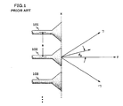
- FIG. 1 shows one such waveguide array comprising three waveguides 101-103 directed into the x-z plane as shown. The waveguides are separated by a distance "a" between the central axis of adjacent waveguides, as shown.
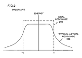
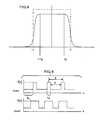
- a figure of merit for such a waveguide array is the radiated power density P( ⁇ ) as a function of ⁇ , the angle from the z-axis. This is measured by exciting one of the waveguides in the array, i.e. waveguide 102, with the fundamental input mode of the waveguide, and then measuring the radiated pattern. Ideally, it is desired to produce a uniform power distribution as shown in ideal response 202 of FIG.
- phased array antenna The operation of a prior art phased array antenna can be described as follows.
- the input to each waveguide of FIG. 1 is excited with the fundamental mode of the input waveguides.
- the signal supplied to each waveguide is initially uncoupled from the signals supplied to the other waveguides and at a separate phase, such that a constant phase difference ⁇ is produced between adjacent waveguides.
- waveguide 101 could be excited with a signal at zero phase, waveguide 102 with the same signal, at 5° phase, waveguide 103 with the same signal at 10° phase, and so forth for the remaining waveguides in the array (not shown). This would imply a phase difference of 5° between any two adjacent waveguides.
- the input wave produced by this excitation is known as the fundamental Bloch mode, or linear phase progression excitation.
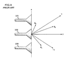
- the direction of ⁇ 0, and consequently of all the other plane waves emanating from the waveguide array, can be adjusted by adjusting the phase difference ⁇ between the inputs to adjacent elements. It can be shown that the fraction of the power radiated at direction ⁇ 0 when the inputs are excited in a linear phase progression is N( ⁇ ), defined previously herein for the case of excitation of only one of the waveguides with the fundamental mode.
- the fractional radiated power outside the central Brillouin zone of FIG. 2, or equivalently, the percentage of the power radiated in directions other than ⁇ 0 in FIG. 3, should be minimized in order to maximize performance.
- false detection could result from the power radiated in directions other than ⁇ 0.
- the wavefront in the direction ⁇ 1 of FIG. 3 comprises most of the unwanted power.
- the problem that remains in the prior art is to provide a waveguide array which, when excited with a Bloch mode, can confine a large portion of its radiated power to the direction ⁇ 0 without using a large number of waveguides. Equivalently, the problem is to provide a waveguide array such that when one waveguide is excited with the fundamental mode, a large portion of the radiated power will be uniformly distributed over the central Brillouin zone.
- the foregoing problem in the prior art has been solved in accordance with the present invention which relates to a highly efficient waveguide array formed by shaping each of the waveguides in an appropriate manner, or equivalently, aligning the waveguides in accordance with a predetermined pattern.
- the predetermined shape or alignment serves to gradually increase the coupling between each waveguide and the adjacent waveguides as the wave propagates through the waveguide array towards the radiating end of the array. The efficiency is maintained regardless of waveguide spacing.
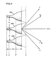
- FIG. 4 shows a waveguide array in accordance with the present invention comprising three waveguides 401-403.
- a ⁇ 0 is chosen, and represents some field of view within the central Brillouin zone over which it is desired to maximize performance.
- the choice of ⁇ 0 will effect the level to which performance can be maximized.
- FIG. 5 shows the response curve of FIG. 2, with an exemplary choice of ⁇ 0. Assuming ⁇ 0 has been chosen, the design of the array is more fully described below.
- the energy in each waveguide is gradually coupled with the energy in the other waveguides.
- This coupling produces a plane wave in a specified direction which is based on the phase difference of the input signals.
- the gradual transition from uncoupled signals to a plane wave also causes unwanted higher order Bloch modes to be generated in the waveguide array, and each unwanted mode produces a plane wave in an undesired direction.
- the directions of these unwanted modes are specified by Equation (2) above.
- These unwanted plane waves, called space harmonics reduce the power in the desired direction.
- the efficiency of the waveguide my is substantially maximized by recognizing that most of the energy radiated in the unwanted directions is radiated in the direction of ⁇ 1.
- the design philosophy is to minimize the energy transferred from the fundamental Bloch mode to the first higher order Bloch mode, denoted the first unwanted mode, as the energy propagates through the waveguide my. This is accomplished by taking advantage of the difference in propagation constants of the fundamental mode and the first unwanted mode.
- each waveguide shown in FIG. 4
- the gradual taper in each waveguide can be viewed as an infinite series of infinitely small discontinuities, each of which causes some energy to be transferred from the fundamental mode to the first unwanted mode.
- the energy transferred from the fundamental mode to the first unwanted mode by each discontinuity will reach the aperture end of the waveguide array at a different phase.
- the waveguide taper should be designed such that the phase of the energy shifted into the first unwanted mode by the different discontinuities is essentially uniformly distributed between zero and 2 ⁇ . If the foregoing condition is satisfied, all the energy in the first unwanted mode will destructively interfere. The design procedure for the taper is more fully described below.
- each of the graphs of FIG. 6 is defined herein as a refractive-space profile of the waveguide array.
- the designations n1 and n2 in FIG. 6 represent the index of refraction between waveguides and within waveguides respectively.
- each plot is a periodic square wave with amplitude proportional to the square of the index of refraction at the particular point in question along the x axis.
- Specifying the shape of these plots at various closely spaced points along the z-axis uniquely determines the shape of the waveguides to be used.
- the problem reduces to one of specifying the plots of FIG. 6 at small intervals along the length of the waveguide. The closer the spacing of the intervals, the more accurate the design. In practical applications, fifty or more such plots, equally spaced, will suffice.
- V(z) the coefficient of the lowest order Fourier term
- V(z) is of interest for the following reasons:
- the phase difference v between the first unwanted mode produced by the aperture of the waveguide array and the first unwanted mode produced by a section dz located at some arbitrary point along the waveguide array is ⁇ (B0 - B1)dz. (4) where the integral is taken over the distance from the arbitrary point to the array aperture, and B0 and B1 are the propagation constants of the fundamental and first unwanted mode respectively.
- Equation 12 can be utilized to specify l(z) at various points along the z axis and thereby define the shape of the waveguides.
- equation (3) becomes where a x is the spacing between waveguide centers in the x direction, and a y is the spacing between waveguide centers in the y direction.
- V 1,0 the first order Fourier coefficient in the x direction.
- this coefficient is calculated by using a two-dimensional Fourier transform.
- the method set forth previously can be utilized to maximize the efficiency in the x direction.
- a x in the left side of equation (14) can be replaced by a y , the spacing between waveguide centers in the second dimension, and the same methods applied to the second dimension.
- the waveguides need not be aligned in perpendicular rows and columns of the x,y plane. Rather, they may be aligned in several rows which are offset from one another or in any planar pattern. However, in that case, the exponent of the two-dimensional Fourier series of equation (14) would be calculated in a slightly different manner in order to account for the angle between the x and y axes. Techniques for calculating a two-dimensional Fourier series when the basis is not two perpendicular vectors are well-known in the art and can be used to practice this invention.
Landscapes
- Variable-Direction Aerials And Aerial Arrays (AREA)
- Optical Integrated Circuits (AREA)
- Control Of Motors That Do Not Use Commutators (AREA)
- Optical Communication System (AREA)
- Light Guides In General And Applications Therefor (AREA)
- Optical Fibers, Optical Fiber Cores, And Optical Fiber Bundles (AREA)
Abstract
Description
- This invention relates to waveguides, and more particularly, a technique for maximinng the efficiency of an array of waveguides.
- Waveguide arrays are used in a wide variety of applications such as phased array antennas and optical star couplers. FIG. 1 shows one such waveguide array comprising three waveguides 101-103 directed into the x-z plane as shown. The waveguides are separated by a distance "a" between the central axis of adjacent waveguides, as shown. A figure of merit for such a waveguide array is the radiated power density P(ϑ) as a function of ϑ, the angle from the z-axis. This is measured by exciting one of the waveguides in the array, i.e.
waveguide 102, with the fundamental input mode of the waveguide, and then measuring the radiated pattern. Ideally, it is desired to produce a uniform power distribution as shown inideal response 202 of FIG. 2, when (γ) is specified by the well-known equation
[a]sin(γ)=λ/2, (1)
where λ is the wavelength of the radiated power in the medium occupying the positive z plane of FIG. 1. The angular distance from -γ to γ is known as the central Brillouin zone. In practice, it is impossible to produce ideal results. An exemplary response from an actual array would look more like typicalactual response 201 of FIG. 2. The efficiency of the array, N(ϑ), when one waveguide is excited, is the ratio of the actual response divided by the ideal response, for all ϑ such that -γ≦ϑ≦γ. Of course, this neglects waveguide attenuation and reflection losses. With this background, the operation of phased array antennas is discussed below. - The operation of a prior art phased array antenna can be described as follows. The input to each waveguide of FIG. 1 is excited with the fundamental mode of the input waveguides. The signal supplied to each waveguide is initially uncoupled from the signals supplied to the other waveguides and at a separate phase, such that a constant phase difference φ is produced between adjacent waveguides. For example, in FIG. 1,
waveguide 101 could be excited with a signal at zero phase, waveguide 102 with the same signal, at 5° phase,waveguide 103 with the same signal at 10° phase, and so forth for the remaining waveguides in the array (not shown). This would imply a phase difference of 5° between any two adjacent waveguides. The input wave produced by this excitation is known as the fundamental Bloch mode, or linear phase progression excitation. When the input excitation is the fundamental Bloch mode, the output from the waveguide array, part of which is illustrated in FIG. 3, will be a series of plane waves, e.g., at directions ϑ₀,ϑ₁ and ϑ₂, each in a difgferent direction, where the direction of the mth plane wave is specified by:
ksin(ϑm)=ksin(ϑ₀)+m [
and the wavefront radiated in the direction of ϑ₀ is the only wavefront in the central Brillouin zone and is specified by the relationship φ = kasin(ϑ₀), m=± 1, ± 2...., and k = 2π/λ in the medium occupying the positive z plane. The direction of ϑ₀, and consequently of all the other plane waves emanating from the waveguide array, can be adjusted by adjusting the phase difference φ between the inputs to adjacent elements. It can be shown that the fraction of the power radiated at direction ϑ₀ when the inputs are excited in a linear phase progression is N(ϑ), defined previously herein for the case of excitation of only one of the waveguides with the fundamental mode. - The relationship between the response of the array to excitation of a single waveguide with the fundamental mode, and the response of the array to the fundamental Bloch mode can be further understood by way of example. Suppose in a Bloch mode excitation φ is adjusted according to φ=kasin ϑ₀ such that ϑ₀ is 5°
- The power radiated at 5° divided by the total input power = N(5°). However, if only one waveguide is excited, and a response similar to
response 201 of FIG. 2 is produced in the Brillouin zone, then at ϑ=5°, P(ϑ)actual/P(ϑ)ideal=N(5°). - The fractional radiated power outside the central Brillouin zone of FIG. 2, or equivalently, the percentage of the power radiated in directions other than ϑ₀ in FIG. 3, should be minimized in order to maximize performance. In a phased array radar antenna, for example, false detection could result from the power radiated in directions other than ϑ₀. It can be shown then that the wavefront in the direction ϑ₁ of FIG. 3 comprises most of the unwanted power. Thus, it is a goal of many prior art waveguide arrays, and of this invention, to eliminate as much as possible of the power radiated in the ϑ₁ direction, and thus provide a high efficiency waveguide array.
- Prior art waveguide arrays have attempted to attain the goal stated above in several ways. One such prior art array is described in N. Amitay et al., Theory and Analysis of Phased Antennas, New York, Wiley Publisher, 1972, at pp. 10-14. The array achieves the goal by setting the spacing between the waveguide centers equal to λ/2 or less. This forces γ to be at least 90°, and thus the central order Brillouin zone occupies the entire real space in the positive z plane of FIG. 1. This method, however, makes it difficult to aim the beam in a narrow desired direction, even with a large number of waveguides. The problem that remains in the prior art is to provide a waveguide array which, when excited with a Bloch mode, can confine a large portion of its radiated power to the direction ϑ₀ without using a large number of waveguides. Equivalently, the problem is to provide a waveguide array such that when one waveguide is excited with the fundamental mode, a large portion of the radiated power will be uniformly distributed over the central Brillouin zone.
- The foregoing problem in the prior art has been solved in accordance with the present invention which relates to a highly efficient waveguide array formed by shaping each of the waveguides in an appropriate manner, or equivalently, aligning the waveguides in accordance with a predetermined pattern. The predetermined shape or alignment serves to gradually increase the coupling between each waveguide and the adjacent waveguides as the wave propagates through the waveguide array towards the radiating end of the array. The efficiency is maintained regardless of waveguide spacing.
-
- FIG. 1 shows an exemplary waveguide array of the prior art;
- FIG. 2 shows the desired response and a typical actual response to the excitation of a single waveguide in the array of FIG. 1;
- FIG. 3 shows a typical response to the excitation of all the waveguides of FIG. 1 in a Bloch mode;
- FIG. 4 shows an exemplary waveguide array in accordance with the present invention;
- FIG. 5 shows the response to the waveguide array of FIG. 4 as compared to that of an ideal array;
- FIG. 6 shows, as a function of x, the refractive space profiles of the waveguide array in two separate planes orthogonal to the longitudinal axis; and
- FIG. 7 shows an alternative embodiment of the inventive waveguide array.
- FIG. 4 shows a waveguide array in accordance with the present invention comprising three waveguides 401-403. The significance of the points z=s,t,c, and c′ will be explained later herein, as will the dashed portion of the waveguides to the right of the apertures of the waveguides at the x axis. In practical arrays, it is impossible to achieve perfect performance throughout the central Brillouin zone. Therefore, a γ₀ is chosen, and represents some field of view within the central Brillouin zone over which it is desired to maximize performance. As will be shown hereinafter, the choice of γ₀ will effect the level to which performance can be maximized. A procedure for choosing the "best" γ₀ is also discussed hereafter. FIG. 5 shows the response curve of FIG. 2, with an exemplary choice of γ₀. Assuming γ₀ has been chosen, the design of the array is more fully described below.
- Returning to FIG. 3, as the fundamental Bloch mode propagates in the positive z direction through the waveguide array, the energy in each waveguide is gradually coupled with the energy in the other waveguides. This coupling produces a plane wave in a specified direction which is based on the phase difference of the input signals. However, the gradual transition from uncoupled signals to a plane wave also causes unwanted higher order Bloch modes to be generated in the waveguide array, and each unwanted mode produces a plane wave in an undesired direction. The directions of these unwanted modes are specified by Equation (2) above. These unwanted plane waves, called space harmonics, reduce the power in the desired direction. The efficiency of the waveguide my is substantially maximized by recognizing that most of the energy radiated in the unwanted directions is radiated in the direction of ϑ₁. As described previously, energy radiated in the direction of ϑ₁ is a direct result of energy converted to the first higher order Bloch mode as the fundamental Bloch mode propagates through the waveguide array. Thus, the design philosophy is to minimize the energy transferred from the fundamental Bloch mode to the first higher order Bloch mode, denoted the first unwanted mode, as the energy propagates through the waveguide my. This is accomplished by taking advantage of the difference in propagation constants of the fundamental mode and the first unwanted mode.
- The gradual taper in each waveguide, shown in FIG. 4, can be viewed as an infinite series of infinitely small discontinuities, each of which causes some energy to be transferred from the fundamental mode to the first unwanted mode. However, because of the difference in propagation constants between the two modes, the energy transferred from the fundamental mode to the first unwanted mode by each discontinuity will reach the aperture end of the waveguide array at a different phase. The waveguide taper should be designed such that the phase of the energy shifted into the first unwanted mode by the different discontinuities is essentially uniformly distributed between zero and 2π. If the foregoing condition is satisfied, all the energy in the first unwanted mode will destructively interfere. The design procedure for the taper is more fully described below.
- FIG.6 shows a plot of the function n²a²[

- Referring to FIG. 6, note that each plot can be expanded into a Fourier series

- Of interest is the coefficient of the lowest order Fourier term V₁ from the above sum. The magnitude of V₁ is denoted herein as V(z).
- V(z) is of interest for the following reasons: The phase difference v between the first unwanted mode produced by the aperture of the waveguide array and the first unwanted mode produced by a section dz located at some arbitrary point along the waveguide array is
∫(B₀ - B₁)dz. (4)
where the integral is taken over the distance from the arbitrary point to the array aperture, and B₀ and B₁ are the propagation constants of the fundamental and first unwanted mode respectively. The total amplitude of the first unwanted mode at the array aperture is


- In order to maximize the efficiency of the array, the width of the waveguides, and thus the duty cycle in the corresponding plot, V(z) should be chosen such that at any point z along the length of the waveguide array, V(z) substantially satisfies the relationship
 )+Ft, L is the length of the waveguide after truncating, i.e., excluding the dashed portion in FIG. 4, Fr and Ft are the fractions of the waveguide remaining and truncated, respectively. More particularly, the length of the waveguide before truncation would include the dashed portion of each waveguide, shown in FIG. 4. This can be calculated easily since, at the point when the waveguides are tangent, (z=t in FIG.4), V(z) will equal 0 as the plot n²a² [

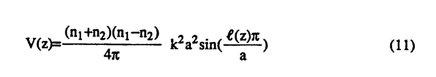

- Thus, after specifying ϑB and γ₀ and, assuming that Ft=0, Equation 12 can be utilized to specify ℓ(z) at various points along the z axis and thereby define the shape of the waveguides.
- Throughout the previous discussion, three assumptions have been made. First, it has been assumed that γ₀ was chosen prior to the design and the efficiency was maximized over the chosen field of view. Next, ϑB was assumed to be an arbitrary angle in the central Brillouin zone. Finally, Ft was assumed to be zero, corresponding to an untruncated waveguide. In actuality, all of these three parameters interact in a complex manner to influence the performance of the array. Further, the performance may even be defined in a manner different from that above. Therefore, an example is provided below of the design of a star coupler. It is to be understood that the example given below is for illustrative purposes of demonstrating the design procedure may be utilized in a wide variety of other applications.
- One figure of merit, M, for an optical star coupler is defined as

- To maximize M, the procedure is as follows: Assume Ft=0, choose an arbitrary ϑB, and calculate N(ϑ) using equations 5-8, for all angles a within the Brillouin zone. Having obtained these values of N(ϑ), vary γ₀ between zero and γ to maximize M. This gives the maximum M for a given Ft and a given ϑB. Next, keeping Ft equal to zero, the same process is iterated using various ϑB's until every ϑB within the Brillouin zone has been tried. This gives the maximum M for a given Ft over all ϑBs. Finally, iterate the entire process with various Ft's until the maximum M is achieved over all ϑBs and Fts. This can be carried out using a computer program.
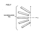
- It should be noted that the example given herein is for illustrative purposes only, and that other variations are possible without violating the scope or spirit of the invention. For example, note from equation 12 that the required property of V(z) can be satisfied by varying "a" as the waveguide is traversed, rather than varying ℓ as is suggested herein. Such an embodiment is shown in FIG. 7, and can be designed using the same methodology and the equations given above. Further, the value of the retractive index, n, could vary at different points in the waveguide cross-section such that equation (12) is satisfied. Applications to radar, optics, microwave, etc. are easily implemented by one of ordinary in the art.
- The invention can also be implemented using a two-dimensional array of waveguides, rather than the one-dimensional array described herein. For the two-dimensional case, equation (3) becomes

- The waveguides need not be aligned in perpendicular rows and columns of the x,y plane. Rather, they may be aligned in several rows which are offset from one another or in any planar pattern. However, in that case, the exponent of the two-dimensional Fourier series of equation (14) would be calculated in a slightly different manner in order to account for the angle between the x and y axes. Techniques for calculating a two-dimensional Fourier series when the basis is not two perpendicular vectors are well-known in the art and can be used to practice this invention.
Claims (8)
a plurality of waveguides, each waveguide including an input port at a first end thereof for receiving electromagnetic energy
and an output port at a second end thereof for launching the electromagnetic energy, the waveguide array including a predetermined series of refractive-space profiles arranged at spaced-apart locations across the waveguide array, each refractive-space profile including a separate Fourier series expansion which comprises a lowest order Fourier term that is determined to substantially maximise the associated efficiency of the waveguide array.

p(y)=
y=Fr(
Applications Claiming Priority (2)
| Application Number | Priority Date | Filing Date | Title |
|---|---|---|---|
| US07/440,825 US5039993A (en) | 1989-11-24 | 1989-11-24 | Periodic array with a nearly ideal element pattern |
| US440825 | 1989-11-24 |
Publications (3)
| Publication Number | Publication Date |
|---|---|
| EP0430516A2 true EP0430516A2 (en) | 1991-06-05 |
| EP0430516A3 EP0430516A3 (en) | 1991-12-18 |
| EP0430516B1 EP0430516B1 (en) | 1997-08-20 |
Family
ID=23750330
Family Applications (1)
| Application Number | Title | Priority Date | Filing Date |
|---|---|---|---|
| EP90312521A Expired - Lifetime EP0430516B1 (en) | 1989-11-24 | 1990-11-16 | A periodic array with a nearly ideal element pattern |
Country Status (6)
| Country | Link |
|---|---|
| US (1) | US5039993A (en) |
| EP (1) | EP0430516B1 (en) |
| JP (1) | JPH03201705A (en) |
| KR (1) | KR940002994B1 (en) |
| CA (1) | CA2030640C (en) |
| DE (1) | DE69031299T2 (en) |
Families Citing this family (31)
| Publication number | Priority date | Publication date | Assignee | Title |
|---|---|---|---|---|
| US5136671A (en) * | 1991-08-21 | 1992-08-04 | At&T Bell Laboratories | Optical switch, multiplexer, and demultiplexer |
| US5412744A (en) * | 1994-05-02 | 1995-05-02 | At&T Corp. | Frequency routing device having a wide and substantially flat passband |
| US5467418A (en) * | 1994-09-02 | 1995-11-14 | At&T Ipm Corp. | Frequency routing device having a spatially filtered optical grating for providing an increased passband width |
| US5926298A (en) * | 1996-08-30 | 1999-07-20 | Lucent Technologies Inc. | Optical multiplexer/demultiplexer having a broadcast port |
| EP0879465B1 (en) * | 1996-11-07 | 2005-11-16 | Koninklijke Philips Electronics N.V. | Data processing of a bitstream signal |
| US6016375A (en) * | 1997-01-08 | 2000-01-18 | Hill; Kenneth O. | Wavelength selective fiber to fiber optical tap |
| US6049644A (en) * | 1997-05-13 | 2000-04-11 | Lucent Technologies Inc. | Optical routing device having a substantially flat passband |
| US5889906A (en) * | 1997-05-28 | 1999-03-30 | Lucent Technologies Inc. | Signal router with coupling of multiple waveguide modes for provicing a shaped multi-channel radiation pattern |
| US6043791A (en) * | 1998-04-27 | 2000-03-28 | Sensis Corporation | Limited scan phased array antenna |
| US6211837B1 (en) * | 1999-03-10 | 2001-04-03 | Raytheon Company | Dual-window high-power conical horn antenna |
| US6493487B1 (en) | 2000-07-14 | 2002-12-10 | Applied Wdm, Inc. | Optical waveguide transmission devices |
| US6434303B1 (en) | 2000-07-14 | 2002-08-13 | Applied Wdm Inc. | Optical waveguide slab structures |
| US6553165B1 (en) | 2000-07-14 | 2003-04-22 | Applied Wdm, Inc. | Optical waveguide gratings |
| US6563997B1 (en) | 2000-11-28 | 2003-05-13 | Lighteross, Inc. | Formation of a surface on an optical component |
| US6596185B2 (en) | 2000-11-28 | 2003-07-22 | Lightcross, Inc. | Formation of optical components on a substrate |
| US7113704B1 (en) | 2000-11-28 | 2006-09-26 | Kotura, Inc. | Tunable add/drop node for optical network |
| US6823096B2 (en) * | 2001-01-05 | 2004-11-23 | Lucent Technologies Inc. | Broadband optical switching arrangements with very low crosstalk |
| US6792180B1 (en) | 2001-03-20 | 2004-09-14 | Kotura, Inc. | Optical component having flat top output |
| US20020158046A1 (en) * | 2001-04-27 | 2002-10-31 | Chi Wu | Formation of an optical component |
| US20020158047A1 (en) * | 2001-04-27 | 2002-10-31 | Yiqiong Wang | Formation of an optical component having smooth sidewalls |
| US6853773B2 (en) * | 2001-04-30 | 2005-02-08 | Kotusa, Inc. | Tunable filter |
| US6614965B2 (en) | 2001-05-11 | 2003-09-02 | Lightcross, Inc. | Efficient coupling of optical fiber to optical component |
| US6674929B2 (en) | 2001-06-01 | 2004-01-06 | Lightcross, Inc. | Tunable optical filter |
| US20020181869A1 (en) * | 2001-06-01 | 2002-12-05 | Wenhua Lin | Tunable dispersion compensator |
| US20030012537A1 (en) * | 2001-07-11 | 2003-01-16 | Chi Wu | Method of forming an optical component |
| US6614951B2 (en) | 2001-08-06 | 2003-09-02 | Lightcross, Inc. | Optical component having a flat top output |
| US6853797B2 (en) * | 2001-11-05 | 2005-02-08 | Kotura, Inc. | Compact optical equalizer |
| US20030091291A1 (en) * | 2001-11-15 | 2003-05-15 | Sam Keo | Smoothing facets on an optical component |
| US6714704B2 (en) | 2001-11-29 | 2004-03-30 | Lightcross, Inc. | Optical component having selected bandwidth |
| US6810168B1 (en) | 2002-05-30 | 2004-10-26 | Kotura, Inc. | Tunable add/drop node |
| US6885795B1 (en) | 2002-05-31 | 2005-04-26 | Kotusa, Inc. | Waveguide tap monitor |
Family Cites Families (14)
| Publication number | Priority date | Publication date | Assignee | Title |
|---|---|---|---|---|
| USRE23051E (en) * | 1948-11-23 | Broadcast antenna | ||
| US2920322A (en) * | 1956-08-28 | 1960-01-05 | Jr Burton P Brown | Antenna system |
| US3243713A (en) * | 1962-12-31 | 1966-03-29 | United Aircraft Corp | Integrated magneto-hydrodynamic generator-radio frequency generator |
| JPS4859754A (en) * | 1971-11-25 | 1973-08-22 | ||
| US3977006A (en) * | 1975-05-12 | 1976-08-24 | Cutler-Hammer, Inc. | Compensated traveling wave slotted waveguide feed for cophasal arrays |
| JPS5344151A (en) * | 1976-10-04 | 1978-04-20 | Mitsubishi Electric Corp | Horn-type antenna |
| GB1562904A (en) * | 1977-06-15 | 1980-03-19 | Marconi Co Ltd | Horns |
| US4259674A (en) * | 1979-10-24 | 1981-03-31 | Bell Laboratories | Phased array antenna arrangement with filtering to reduce grating lobes |
| US4369413A (en) * | 1981-02-03 | 1983-01-18 | The United States Of America As Represented By The Secretary Of The Navy | Integrated dual taper waveguide expansion joint |
| FR2518826A1 (en) * | 1981-12-18 | 1983-06-24 | Thomson Csf | Monomode microwave-radiating horn for radar or telecommunication - has progressive and continuous decrease of slope along axis from 90 degrees or less towards zero at opening |
| US4878059A (en) * | 1983-08-19 | 1989-10-31 | Spatial Communications, Inc. | Farfield/nearfield transmission/reception antenna |
| JPS60196003A (en) * | 1984-03-19 | 1985-10-04 | Nippon Telegr & Teleph Corp <Ntt> | Multi-beam antenna of low side lobe |
| US4737004A (en) * | 1985-10-03 | 1988-04-12 | American Telephone And Telegraph Company, At&T Bell Laboratories | Expanded end optical fiber and associated coupling arrangements |
| JP2585268B2 (en) * | 1987-05-15 | 1997-02-26 | 株式会社東芝 | Reflector antenna |
-
1989
- 1989-11-24 US US07/440,825 patent/US5039993A/en not_active Expired - Lifetime
-
1990
- 1990-11-16 DE DE69031299T patent/DE69031299T2/en not_active Expired - Fee Related
- 1990-11-16 EP EP90312521A patent/EP0430516B1/en not_active Expired - Lifetime
- 1990-11-22 JP JP2320534A patent/JPH03201705A/en active Pending
- 1990-11-22 CA CA002030640A patent/CA2030640C/en not_active Expired - Fee Related
- 1990-11-23 KR KR1019900019060A patent/KR940002994B1/en not_active Expired - Fee Related
Also Published As
| Publication number | Publication date |
|---|---|
| JPH03201705A (en) | 1991-09-03 |
| CA2030640C (en) | 1995-01-17 |
| CA2030640A1 (en) | 1991-05-25 |
| KR940002994B1 (en) | 1994-04-09 |
| DE69031299D1 (en) | 1997-09-25 |
| EP0430516A3 (en) | 1991-12-18 |
| US5039993A (en) | 1991-08-13 |
| DE69031299T2 (en) | 1997-12-18 |
| EP0430516B1 (en) | 1997-08-20 |
| KR910010769A (en) | 1991-06-29 |
Similar Documents
| Publication | Publication Date | Title |
|---|---|---|
| US5039993A (en) | Periodic array with a nearly ideal element pattern | |
| EP0563067B1 (en) | Optical device | |
| Yeh et al. | The essence of dielectric waveguides | |
| US5002350A (en) | Optical multiplexer/demultiplexer | |
| Rahman et al. | Analysis of optical waveguide discontinuities | |
| Chiou et al. | Analysis of optical waveguide discontinuities using the Padé approximants | |
| US4091387A (en) | Beam forming network | |
| EP0308502B1 (en) | Ideal distributed bragg reflectors and resonators | |
| Yoneta et al. | Combination of beam propagation method and finite element method for optical beam propagation analysis | |
| Skobelev et al. | Optimum geometry and performance of a dual-mode horn modification | |
| Bird | Mode matching analysis of arrays of stepped rectangular horns and application to satellite antenna design | |
| Kalhor et al. | Scattering of waves by gratings of conducting cylinders | |
| Makeev et al. | Analysis and optimization of an array of miltimode plane waveguides excited by TM waves in order to form sectorial partial directional patterns | |
| Encinar | Analysis and CAD techniques for periodic leaky‐wave printed antennas: Numerical and experimental results | |
| Provalov et al. | Investigations of the fields in a bounded planar dielectric waveguide | |
| Dubost et al. | Propagation along two radiating coupled waveguides: Applications to a multimode radiating array | |
| Sammut et al. | Graded monomode fibres and planar waveguides | |
| Miyanaga et al. | Intensity profiles of outgoing beams from tapered grating couplers | |
| Checcacci et al. | Modes and instabilities of modes of the flat-roof open resonator | |
| Shishegar et al. | A hybrid analysis method for planar lens-like structures | |
| Vorobjov et al. | A quasioptical directional coupler on diffraction-coupled transmission lines | |
| Vzyatyshev et al. | Dielectric waveguides and waveguide devices for microwave applications | |
| Granet et al. | New method for analysis of constrained metal plate lens | |
| Kusano et al. | Bending loss formulas for step‐index optical fiber and their applicable regions | |
| Derneryd | Multielement phased array waveguide simulator for circular polarization |
Legal Events
| Date | Code | Title | Description |
|---|---|---|---|
| PUAI | Public reference made under article 153(3) epc to a published international application that has entered the european phase |
Free format text: ORIGINAL CODE: 0009012 |
|
| AK | Designated contracting states |
Kind code of ref document: A2 Designated state(s): DE GB IT NL |
|
| PUAL | Search report despatched |
Free format text: ORIGINAL CODE: 0009013 |
|
| AK | Designated contracting states |
Kind code of ref document: A3 Designated state(s): DE GB IT NL |
|
| 17P | Request for examination filed |
Effective date: 19920610 |
|
| 17Q | First examination report despatched |
Effective date: 19940422 |
|
| RAP3 | Party data changed (applicant data changed or rights of an application transferred) |
Owner name: AT&T CORP. |
|
| GRAG | Despatch of communication of intention to grant |
Free format text: ORIGINAL CODE: EPIDOS AGRA |
|
| GRAH | Despatch of communication of intention to grant a patent |
Free format text: ORIGINAL CODE: EPIDOS IGRA |
|
| GRAH | Despatch of communication of intention to grant a patent |
Free format text: ORIGINAL CODE: EPIDOS IGRA |
|
| GRAA | (expected) grant |
Free format text: ORIGINAL CODE: 0009210 |
|
| AK | Designated contracting states |
Kind code of ref document: B1 Designated state(s): DE GB IT NL |
|
| ITF | It: translation for a ep patent filed | ||
| REF | Corresponds to: |
Ref document number: 69031299 Country of ref document: DE Date of ref document: 19970925 |
|
| PLBE | No opposition filed within time limit |
Free format text: ORIGINAL CODE: 0009261 |
|
| STAA | Information on the status of an ep patent application or granted ep patent |
Free format text: STATUS: NO OPPOSITION FILED WITHIN TIME LIMIT |
|
| 26N | No opposition filed | ||
| PGFP | Annual fee paid to national office [announced via postgrant information from national office to epo] |
Ref country code: GB Payment date: 19991026 Year of fee payment: 10 |
|
| PGFP | Annual fee paid to national office [announced via postgrant information from national office to epo] |
Ref country code: NL Payment date: 19991027 Year of fee payment: 10 |
|
| PGFP | Annual fee paid to national office [announced via postgrant information from national office to epo] |
Ref country code: DE Payment date: 19991231 Year of fee payment: 10 |
|
| PG25 | Lapsed in a contracting state [announced via postgrant information from national office to epo] |
Ref country code: GB Free format text: LAPSE BECAUSE OF NON-PAYMENT OF DUE FEES Effective date: 20001116 |
|
| PG25 | Lapsed in a contracting state [announced via postgrant information from national office to epo] |
Ref country code: NL Free format text: LAPSE BECAUSE OF NON-PAYMENT OF DUE FEES Effective date: 20010601 |
|
| GBPC | Gb: european patent ceased through non-payment of renewal fee |
Effective date: 20001116 |
|
| NLV4 | Nl: lapsed or anulled due to non-payment of the annual fee |
Effective date: 20010601 |
|
| PG25 | Lapsed in a contracting state [announced via postgrant information from national office to epo] |
Ref country code: DE Free format text: LAPSE BECAUSE OF NON-PAYMENT OF DUE FEES Effective date: 20010801 |
|
| PG25 | Lapsed in a contracting state [announced via postgrant information from national office to epo] |
Ref country code: IT Free format text: LAPSE BECAUSE OF NON-PAYMENT OF DUE FEES;WARNING: LAPSES OF ITALIAN PATENTS WITH EFFECTIVE DATE BEFORE 2007 MAY HAVE OCCURRED AT ANY TIME BEFORE 2007. THE CORRECT EFFECTIVE DATE MAY BE DIFFERENT FROM THE ONE RECORDED. Effective date: 20051116 |