EP0429728B1 - Logic circuit - Google Patents
Logic circuit Download PDFInfo
- Publication number
- EP0429728B1 EP0429728B1 EP89312532A EP89312532A EP0429728B1 EP 0429728 B1 EP0429728 B1 EP 0429728B1 EP 89312532 A EP89312532 A EP 89312532A EP 89312532 A EP89312532 A EP 89312532A EP 0429728 B1 EP0429728 B1 EP 0429728B1
- Authority
- EP
- European Patent Office
- Prior art keywords
- clock signal
- register
- logic
- address
- logic circuit
- Prior art date
- Legal status (The legal status is an assumption and is not a legal conclusion. Google has not performed a legal analysis and makes no representation as to the accuracy of the status listed.)
- Expired - Lifetime
Links
Images



Classifications
-
- G—PHYSICS
- G01—MEASURING; TESTING
- G01R—MEASURING ELECTRIC VARIABLES; MEASURING MAGNETIC VARIABLES
- G01R31/00—Arrangements for testing electric properties; Arrangements for locating electric faults; Arrangements for electrical testing characterised by what is being tested not provided for elsewhere
- G01R31/28—Testing of electronic circuits, e.g. by signal tracer
- G01R31/317—Testing of digital circuits
- G01R31/3181—Functional testing
- G01R31/3185—Reconfiguring for testing, e.g. LSSD, partitioning
- G01R31/318533—Reconfiguring for testing, e.g. LSSD, partitioning using scanning techniques, e.g. LSSD, Boundary Scan, JTAG
- G01R31/318558—Addressing or selecting of subparts of the device under test
-
- G—PHYSICS
- G01—MEASURING; TESTING
- G01R—MEASURING ELECTRIC VARIABLES; MEASURING MAGNETIC VARIABLES
- G01R31/00—Arrangements for testing electric properties; Arrangements for locating electric faults; Arrangements for electrical testing characterised by what is being tested not provided for elsewhere
- G01R31/28—Testing of electronic circuits, e.g. by signal tracer
- G01R31/317—Testing of digital circuits
- G01R31/3181—Functional testing
- G01R31/3185—Reconfiguring for testing, e.g. LSSD, partitioning
- G01R31/318533—Reconfiguring for testing, e.g. LSSD, partitioning using scanning techniques, e.g. LSSD, Boundary Scan, JTAG
- G01R31/318552—Clock circuits details
-
- G—PHYSICS
- G06—COMPUTING OR CALCULATING; COUNTING
- G06F—ELECTRIC DIGITAL DATA PROCESSING
- G06F1/00—Details not covered by groups G06F3/00 - G06F13/00 and G06F21/00
- G06F1/04—Generating or distributing clock signals or signals derived directly therefrom
- G06F1/10—Distribution of clock signals, e.g. skew
-
- G—PHYSICS
- G11—INFORMATION STORAGE
- G11C—STATIC STORES
- G11C19/00—Digital stores in which the information is moved stepwise, e.g. shift registers
Definitions
- the present invention relates to a logic circuit, more specifically, to logic circuit including a clocking arrangement for clocking data through multiple bit registers in the circuit.
- CMOS logic circuits are commonly designed according to a Level Sensitive Scan Design (LSSD) technique. These LSSD circuits are responsive to a combination of a C clock signal and a B clock signal. The C clock signal and the B clock signal are non-overlapping. More specifically, although they are of the same frequency, it is a requirement of LSSD that active periods of the two clock signals do not coincide.
- a register in the logic circuit designed according to an LSSD technique, consists of an array of Shift Register Latches (SRLs).
- An SRL consists of a first latch responsive to the C clock signal and a second latch responsive to the B clock signal. When the C clock signal is true, an input data bit is stored in the first latch.
- clocking a process by which a latch responds to a clock signal by storing a data bit shall hereinafter be referred to as clocking.
- Some synchronous logic circuits include registers for storing dependent data groups such as "set-up" parameters. Such data groups are modified infrequently during normal operation of the logic circuit. When such a data group changes, an address word, associated with the data group, can be generated by combinatorial logic in the logic circuit. The address word can be further decoded by the combinatorial logic to produce a true state in an I/O address line which is otherwise held false. In a similar fashion, other I/O address lines can be associated with other data groups stored in other registers in the synchronous logic circuit. In one such known synchronous logic circuit design, a separate suppression gate corresponds to every register storing a dependent data group.
- the suppression gate prevents the C clock signal from clocking the first latches of a register unless an associated I/O address line is true.
- Such a function is referred to in the art as a gating function.
- This arrangement has the advantage that the use of C clock suppression can reduce the complexity of addressing logic and therefore the cost of combinatorial logic in the logic circuit.
- C clock suppression also provides some reduction in power consumed by the logic circuit.
- the C clock signal to a particular register may be inhibited, because a corresponding I/O address line is false, the B clock signal continues to block the second latches in the registry thereby causing unnecessary power consumption.
- IBM Technical Disclosure Bulletin Vol.18, No.11, April 1976, pages 3711 to 3712 describes a logic circuit comprising a register.
- the register has first register latches to clock data into the register in response to a first clock signal and second register latches to clock data out of the register in response to a second clock signal.
- the first and second clock signals are inhibited or admitted to the first and second register latches in dependence on the state of a block line.
- the aim of the present invention is to provide a clock architecture for minimising the power consumed by a synchronous CMOS logic circuit.
- a logic circuit comprising: a plurality of registers, each register having first register latches to clock data into the register in response to a first clock signal and second register latches to clock data out of the register in response to a second clock signal; address logic to address data to the registers; and first suppression logic connected to the address logic to inhibit the first clock signal input to the registers in response to the address logic; characterised in that the logic circuit further comprises second suppression logic to inhibit the second clock signal input to the registers in collective response to the address logic and the first clock signal.
- a logic circuit in accordance with the present invention has the advantage of providing a second gating function, applicable to the second block signal yet responsive to the first clock signal, by which means data is now only admitted to any register when data stored therein is to change.
- the number of clock transitions undergone by second latches in the logic circuit can now be reduced. Since the first clock signal input to such a register may be subject to a first gating function, a mechanism is provided for further reducing power consumed by a CMOS logic circuit.
- the present invention is broadly applicable to processing logic implemented by Very Large Scale Integration (VLSI) of (e.g CMOS devices) on a silicon substrate.
- VLSI Very Large Scale Integration
- the general logic circuit shown in Figure 1 is symbolic of such processing logic. Therefore, for background information, this general logic circuit, which may include an example of logic in accordance with the present invention, will now be described.
- the general logic circuit consists of a multiple bit register block 3 for data storage and a combinatorial logic network 4 for data processing.
- the multiple bit register block consists of separate registers for storing feedback data 1.
- the feedback data is passed through the multiple bit LSSD register block to the combinational logic in response to a non-overlapping clock stimulus 22, 23 produced by a clock generator 5.
- a non-overlapping clock stimulus 22, 23 produced by a clock generator 5.
- This register structure consists of separate registers for storing data groups associated with the logic circuit.
- register 30 is used to store data group A.
- Data bit a1 of data group A is stored in SRL latch 36.
- First latch 31 of SRL array 36 loads data bit a1 in response to a true state in the C clock signal 37 occurring during a period for which address line Ca is also true.
- AND gate 33 prevents the C clock signal from clocking the first latches in the register when address line Ca is false.
- the register also includes a control latch 34 into which the state of the address line Ca is loaded in response to a true state in the C clock signal.
- Second latch 32 of SRL array 36 loads data bit a1 in response to a true state in the B clock signal 38 occurring during a period for which delayed address line C'a is also true.
- the state of delayed address line C'a is specified by the contents of the control latch.
- AND gate 35 prevents the B clock signal from clocking the second latches in the register when delayed address line C'a is false. More specifically, during a true state in the B clock signal, the state of the delayed address line C'a is the same as that of the address line Ca during the immediately preceding true state of the C clock signal.
- a "look ahead" clock structure is therefore provided whereby the B clock signal only clocks the register in response to the C clock signal previously clocking the register which, in turn, is made possible by switching address line Ca to a true state.
- this "look ahead" clock structure can be implemented in as many registers in the logic circuit as necessary.
- another register 39 for storing data group B has a similar topology to register 30 for storing data group A.
- this example of the "look ahead" clock structure can significantly reduce the number of clock transitions to which registers in the logic circuit are subjected. The degree of power reduction depends on the number of B clock cycles for which the address lines are true.
- the present invention is particularly applicable to those logic circuits comprising a large number of registers for storing "set-up" parameters which are changed infrequently during normal operation.
- FIG. 3 Another LSSD register structure is shown in Figure 3.
- This register structure has a similar "look ahead” clock function to that described in the preceding paragraphs.
- an alternative "look ahead” clock structure is employed.
- This alternative "look ahead” clock structure will now be described with reference to Figure 3 in which register 50 is for storing the data group A as used in the description of the previous example.
- Data bit a1 is stored in SRL 54.
- First latch 55 of SRL 54 loads data bit a1 in response to a true state in the C clock signal occurring during a period for which both address line Ca and I/O write line W 53 are true.
- AND gate 56 prevents the C clock signal from clocking the first latches in register 50 except when I/O write line W and address line Ca are true simultaneously.
- Second latch 57 of SRL array 54 loads data bit a1 in response to a true state in the B clock signal occurring during a period for which delayed I/O write line W' is also true.
- the state of delayed I/O write line W' is specified by the contents an I/O write latch 52 which loads the state of the I/O write line W in response to a true state in the C clock signal.
- AND gate 58 prevents the B clock signal from clocking the second latches in register 50 when the delayed I/O write bit W' is false.
- AND gate 58 and the I/O write latch implement a "look ahead" clock function which can not only prevent the B clock signal from clocking register 50, but also from clocking register 51, which is for storing data group B, and into which data group B can be loaded in only when address line Cb is true during a true state in the C clock signal.
- a "look ahead" clock function can be implemented in as many registers in the logic circuit as necessary via the addition of a single control latch, a single AND gate, and a single additional I/O write bit.
- each register was assigned individual B clock suppression logic consisting of separate latch and AND gate. The example of the present invention described in this paragraph is therefore a less complicated implementation.
- the degree of power reduction provided by this structure depends on the number of B clock cycles for which the I/O write bit is true.
- the I/O write bit is true when signifying a change in data stored in the registers. If the I/O write bit is true more often than it is false, the degree of power reduction will be accordingly small. However, as stated in the preceding paragraphs, such circumstances are unlikely to arise in logic circuits having a large number of registers for storing "set-up" parameters which are changed infrequently during normal operation.
- the clock signal timing diagram shown in Figure 4 illustrates an example phase relationship between the C clock signal 71 and the B clock signal 70 for clocking the register structures shown in Figure 2 and Figure 3.
- Logic circuits produced by interconnecting CMOS devices contain parasitic impedances which give rise to signal delays. Such delays can cause spurious signals to propagate through the logic circuit. It is therefore necessary to define a "settling" interval t1 after each true state 72 of one clock signal during which the other clock signal is held false.
- the register structures described hereinbefore are composed of LSSD register latches; each latch being fabricated by the very large scale integration of CMOS devices. It will be appreciated, however, that the present invention is not limited in application to such logic circuits. Clearly, the present invention is applicable to any logic circuit in which data is processed in response to a set of non overlapping clock signals and from which power is dissipated during periods of transience in such clock signals.
Landscapes
- Engineering & Computer Science (AREA)
- General Engineering & Computer Science (AREA)
- Physics & Mathematics (AREA)
- General Physics & Mathematics (AREA)
- Theoretical Computer Science (AREA)
- Logic Circuits (AREA)
- Shift Register Type Memory (AREA)
- Tests Of Electronic Circuits (AREA)
- Power Sources (AREA)
- Test And Diagnosis Of Digital Computers (AREA)
Description
- The present invention relates to a logic circuit, more specifically, to logic circuit including a clocking arrangement for clocking data through multiple bit registers in the circuit.
- Synchronous Complementary Metal Oxide Semiconductor (CMOS) logic circuits are commonly designed according to a Level Sensitive Scan Design (LSSD) technique. These LSSD circuits are responsive to a combination of a C clock signal and a B clock signal. The C clock signal and the B clock signal are non-overlapping. More specifically, although they are of the same frequency, it is a requirement of LSSD that active periods of the two clock signals do not coincide. A register in the logic circuit, designed according to an LSSD technique, consists of an array of Shift Register Latches (SRLs). An SRL consists of a first latch responsive to the C clock signal and a second latch responsive to the B clock signal. When the C clock signal is true, an input data bit is stored in the first latch. When the B clock signal is true, the input data bit is passed from the first latch and stored in the second latch. For the purpose of explanation, and to highlight aspects of the present invention, a process by which a latch responds to a clock signal by storing a data bit shall hereinafter be referred to as clocking.
- Many synchronous logic circuits include a large number of multiple bit registers and may therefore contain thousands of SRLs. Power consumption problems can arise if such a logic circuit is manufactured by integrating CMOS devices on a silicon substrate. Logic gates consisting of CMOS devices consume most electrical power whilst in transience between logical states. This power is dissipated as heat. Therefore, the power consumed by many thousands of CMOS SRLs, switching on every clock cycle, makes a significant contribution to heat dissipated by a logic circuit. Such heat dissipation can restrict the choice of packaging material for encapsulating the logic circuit to those material with suitable heatsinking properties, which may not be the cheapest materials available. Therefore, since there is a demand for denser device integration and faster clock rates, to increase on-chip processing power, the need has arisen to examine methods for reducing power consumption associated with CMOS device technology.
- Some synchronous logic circuits include registers for storing dependent data groups such as "set-up" parameters. Such data groups are modified infrequently during normal operation of the logic circuit. When such a data group changes, an address word, associated with the data group, can be generated by combinatorial logic in the logic circuit. The address word can be further decoded by the combinatorial logic to produce a true state in an I/O address line which is otherwise held false. In a similar fashion, other I/O address lines can be associated with other data groups stored in other registers in the synchronous logic circuit. In one such known synchronous logic circuit design, a separate suppression gate corresponds to every register storing a dependent data group. The suppression gate prevents the C clock signal from clocking the first latches of a register unless an associated I/O address line is true. Such a function is referred to in the art as a gating function. This arrangement has the advantage that the use of C clock suppression can reduce the complexity of addressing logic and therefore the cost of combinatorial logic in the logic circuit. Furthermore, C clock suppression also provides some reduction in power consumed by the logic circuit. However, while the C clock signal to a particular register may be inhibited, because a corresponding I/O address line is false, the B clock signal continues to block the second latches in the registry thereby causing unnecessary power consumption.
- IBM Technical Disclosure Bulletin Vol.18, No.11, April 1976, pages 3711 to 3712, describes a logic circuit comprising a register. The register has first register latches to clock data into the register in response to a first clock signal and second register latches to clock data out of the register in response to a second clock signal. The first and second clock signals are inhibited or admitted to the first and second register latches in dependence on the state of a block line.
- The aim of the present invention, therefore, is to provide a clock architecture for minimising the power consumed by a synchronous CMOS logic circuit.
- According to the present invention there is now proposed a logic circuit comprising: a plurality of registers, each register having first register latches to clock data into the register in response to a first clock signal and second register latches to clock data out of the register in response to a second clock signal; address logic to address data to the registers; and first suppression logic connected to the address logic to inhibit the first clock signal input to the registers in response to the address logic; characterised in that the logic circuit further comprises second suppression logic to inhibit the second clock signal input to the registers in collective response to the address logic and the first clock signal.
- A logic circuit in accordance with the present invention has the advantage of providing a second gating function, applicable to the second block signal yet responsive to the first clock signal, by which means data is now only admitted to any register when data stored therein is to change. The number of clock transitions undergone by second latches in the logic circuit can now be reduced. Since the first clock signal input to such a register may be subject to a first gating function, a mechanism is provided for further reducing power consumed by a CMOS logic circuit.
- A particular embodiment of the present invention, and aspects of logic circuitry to which the invention relates will now be described with reference to the following diagrams in which:
- Figure 1 is a block diagram of a general logic circuit having an LSSD architecture.
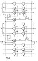
- Figure 2 is a block diagram of an LSSD register structure for the logic circuit.
- Figure 3 is a block diagram of another LSSD register structure for the logic circuit.
- Figure 4 illustrates a timing relationship between the C clock signal and the B clock signal associated with the LSSD architecture.
- The present invention is broadly applicable to processing logic implemented by Very Large Scale Integration (VLSI) of (e.g CMOS devices) on a silicon substrate. The general logic circuit shown in Figure 1 is symbolic of such processing logic. Therefore, for background information, this general logic circuit, which may include an example of logic in accordance with the present invention, will now be described. The general logic circuit consists of a multiple
bit register block 3 for data storage and acombinatorial logic network 4 for data processing. The multiple bit register block consists of separate registers for storingfeedback data 1. The feedback data is passed through the multiple bit LSSD register block to the combinational logic in response to anon-overlapping clock stimulus clock generator 5. As a result of such stimulus and additional input data 6, both the feedback data and data output 8 from the logic circuit can be refreshed. - An LSSD register structure arranged in accordance with the present invention will now be described with reference to Figure 2. This register structure consists of separate registers for storing data groups associated with the logic circuit. For instance,
register 30 is used to store data group A. Data bit a1 of data group A is stored inSRL latch 36.First latch 31 ofSRL array 36 loads data bit a1 in response to a true state in theC clock signal 37 occurring during a period for which address line Ca is also true. ANDgate 33 prevents the C clock signal from clocking the first latches in the register when address line Ca is false. The register also includes acontrol latch 34 into which the state of the address line Ca is loaded in response to a true state in the C clock signal.Second latch 32 ofSRL array 36 loads data bit a1 in response to a true state in theB clock signal 38 occurring during a period for which delayed address line C'a is also true. The state of delayed address line C'a is specified by the contents of the control latch. ANDgate 35 prevents the B clock signal from clocking the second latches in the register when delayed address line C'a is false. More specifically, during a true state in the B clock signal, the state of the delayed address line C'a is the same as that of the address line Ca during the immediately preceding true state of the C clock signal. A "look ahead" clock structure is therefore provided whereby the B clock signal only clocks the register in response to the C clock signal previously clocking the register which, in turn, is made possible by switching address line Ca to a true state. - Referring to Figure 2, it can be seen that this "look ahead" clock structure can be implemented in as many registers in the logic circuit as necessary. For instance, in Figure 2, another
register 39 for storing data group B has a similar topology to register 30 for storing data group A. However, in the case of data group B, the C and B clocksignals clock register 39 subject to the status of address line Cb. Therefore, by way of the present invention, such address lines can now select which registers the B clock signal is applied to, in addition to selecting which registers the C clock signal is applied to. It follows that this example of the "look ahead" clock structure can significantly reduce the number of clock transitions to which registers in the logic circuit are subjected. The degree of power reduction depends on the number of B clock cycles for which the address lines are true. If the address lines are true more often than they are false, the degree of power reduction will be accordingly small. It follows therefore, that the present invention is particularly applicable to those logic circuits comprising a large number of registers for storing "set-up" parameters which are changed infrequently during normal operation. - By way of another example of the present invention, another LSSD register structure is shown in Figure 3. This register structure has a similar "look ahead" clock function to that described in the preceding paragraphs. However in this case an alternative "look ahead" clock structure is employed. This alternative "look ahead" clock structure will now be described with reference to Figure 3 in which register 50 is for storing the data group A as used in the description of the previous example. Data bit a1 is stored in
SRL 54.First latch 55 ofSRL 54 loads data bit a1 in response to a true state in the C clock signal occurring during a period for which both address line Ca and I/Owrite line W 53 are true. AND gate 56 prevents the C clock signal from clocking the first latches inregister 50 except when I/O write line W and address line Ca are true simultaneously.Second latch 57 ofSRL array 54 loads data bit a1 in response to a true state in the B clock signal occurring during a period for which delayed I/O write line W' is also true. The state of delayed I/O write line W' is specified by the contents an I/O write latch 52 which loads the state of the I/O write line W in response to a true state in the C clock signal. ANDgate 58 prevents the B clock signal from clocking the second latches inregister 50 when the delayed I/O write bit W' is false. ANDgate 58 and the I/O write latch implement a "look ahead" clock function which can not only prevent the B clock signal from clockingregister 50, but also from clockingregister 51, which is for storing data group B, and into which data group B can be loaded in only when address line Cb is true during a true state in the C clock signal. In this structure, a "look ahead" clock function can be implemented in as many registers in the logic circuit as necessary via the addition of a single control latch, a single AND gate, and a single additional I/O write bit. By contrast, in the example of the present invention described in the preceding paragraphs, each register was assigned individual B clock suppression logic consisting of separate latch and AND gate. The example of the present invention described in this paragraph is therefore a less complicated implementation. The degree of power reduction provided by this structure depends on the number of B clock cycles for which the I/O write bit is true. The I/O write bit is true when signifying a change in data stored in the registers. If the I/O write bit is true more often than it is false, the degree of power reduction will be accordingly small. However, as stated in the preceding paragraphs, such circumstances are unlikely to arise in logic circuits having a large number of registers for storing "set-up" parameters which are changed infrequently during normal operation. - The clock signal timing diagram shown in Figure 4 illustrates an example phase relationship between the
C clock signal 71 and the B clock signal 70 for clocking the register structures shown in Figure 2 and Figure 3. Logic circuits produced by interconnecting CMOS devices contain parasitic impedances which give rise to signal delays. Such delays can cause spurious signals to propagate through the logic circuit. It is therefore necessary to define a "settling" interval t1 after eachtrue state 72 of one clock signal during which the other clock signal is held false. - For the purpose of illustrating the present invention, the register structures described hereinbefore are composed of LSSD register latches; each latch being fabricated by the very large scale integration of CMOS devices. It will be appreciated, however, that the present invention is not limited in application to such logic circuits. Clearly, the present invention is applicable to any logic circuit in which data is processed in response to a set of non overlapping clock signals and from which power is dissipated during periods of transience in such clock signals.
Claims (6)
- A logic circuit comprising: a plurality of registers (30;50), each register (30;50) having first register latches (31;55) to clock data into the register (30;50) in response to a first clock signal (C) and second register latches (32;57) to clock data out of the register (30;50) in response to a second clock signal (B); address logic (Ca;W) to address data to the registers (30;50); and first suppression logic (33) connected to the address logic to inhibit the first clock signal (C) input to the registers (30;50) in response to the address logic (Ca;W); characterised in that the logic circuit further comprises second suppression logic (34,35;52,58) to inhibit the second clock signal (B) input to the registers (30;50) in collective response to the address logic (Ca;W) and the first clock signal (C).
- A logic circuit as claimed in claim 1 wherein the second suppression logic comprises a plurality of control latches (34,40); each latch corresponding to a register for responding to the first clock signal, by storing an address bit for addressing data to the register; the address bit being generated by the address logic.
- A logic circuit as claimed in claim 2 wherein the second suppression logic comprises a plurality of control gates (35,42); each control gate corresponding to a register for admitting the second clock signal to the register subject to a corresponding control latch containing a particular bit value.
- A logic circuit as claimed in claim 1 wherein the second suppression logic comprises one control latch (52) for responding to the first clock signal by storing a write bit (53) generated by the address logic.
- A logic circuit as claimed in claim 4 wherein the second suppression logic comprises one control gate (58) for admitting the second clock signal to the registers subject to the control latch containing a particular bit value.
- A method of inhibiting the second clock signal in a logic circuit as claimed in claim 1, the method comprising:
generating in the address logic an address bit for addressing data to one or more of the registers;
storing the address bit in a control latch in response to the first clock signal; and
gating the second clock signal by gating means comprising a control gate for admitting the second clock signal to the one or more registers subject to the control latch containing a particular bit value.
Priority Applications (4)
| Application Number | Priority Date | Filing Date | Title |
|---|---|---|---|
| EP89312532A EP0429728B1 (en) | 1989-11-30 | 1989-11-30 | Logic circuit |
| DE68916249T DE68916249T2 (en) | 1989-11-30 | 1989-11-30 | Logic circuit. |
| US07/484,144 US5157286A (en) | 1989-11-30 | 1990-02-23 | Conditional clocking of the second latch of a shift register ratch |
| JP2292236A JPH0766341B2 (en) | 1989-11-30 | 1990-10-31 | Logic circuit |
Applications Claiming Priority (1)
| Application Number | Priority Date | Filing Date | Title |
|---|---|---|---|
| EP89312532A EP0429728B1 (en) | 1989-11-30 | 1989-11-30 | Logic circuit |
Publications (2)
| Publication Number | Publication Date |
|---|---|
| EP0429728A1 EP0429728A1 (en) | 1991-06-05 |
| EP0429728B1 true EP0429728B1 (en) | 1994-06-15 |
Family
ID=8202867
Family Applications (1)
| Application Number | Title | Priority Date | Filing Date |
|---|---|---|---|
| EP89312532A Expired - Lifetime EP0429728B1 (en) | 1989-11-30 | 1989-11-30 | Logic circuit |
Country Status (4)
| Country | Link |
|---|---|
| US (1) | US5157286A (en) |
| EP (1) | EP0429728B1 (en) |
| JP (1) | JPH0766341B2 (en) |
| DE (1) | DE68916249T2 (en) |
Cited By (2)
| Publication number | Priority date | Publication date | Assignee | Title |
|---|---|---|---|---|
| CN100587508C (en) * | 2006-06-29 | 2010-02-03 | 国际商业机器公司 | Scan chain and method for realizing high-speed test circuit |
| CN103454577A (en) * | 2012-05-31 | 2013-12-18 | 国际商业机器公司 | Scan chain structure and method and equipment for diagnosing scan chain |
Families Citing this family (4)
| Publication number | Priority date | Publication date | Assignee | Title |
|---|---|---|---|---|
| US5235600A (en) * | 1991-03-21 | 1993-08-10 | Amdahl Corporation | Scannable system with addressable clock suppress elements |
| JP2744724B2 (en) * | 1991-10-03 | 1998-04-28 | シャープ株式会社 | Packet collection circuit in data flow type system |
| US5444404A (en) * | 1994-03-03 | 1995-08-22 | Vlsi Technology, Inc. | Scan flip-flop with power saving feature |
| US20050151570A1 (en) * | 2002-02-21 | 2005-07-14 | Van Lammeren Johannes P.M. | Integrated circuit having reduced substate bounce |
Family Cites Families (6)
| Publication number | Priority date | Publication date | Assignee | Title |
|---|---|---|---|---|
| US3555433A (en) * | 1968-02-26 | 1971-01-12 | Rca Corp | Bidirectional shift register |
| US4627085A (en) * | 1984-06-29 | 1986-12-02 | Applied Micro Circuits Corporation | Flip-flop control circuit |
| JPS6249457A (en) * | 1985-08-28 | 1987-03-04 | Ascii Corp | Storage unit |
| US4780874A (en) * | 1987-04-20 | 1988-10-25 | Tandem Computers Incorporated | Diagnostic apparatus for a data processing system |
| US4775653A (en) * | 1987-04-28 | 1988-10-04 | Vista Chemical Company | Alkoxylation process using calcium based catalysts |
| US4961013A (en) * | 1989-10-18 | 1990-10-02 | Hewlett-Packard Company | Apparatus for generation of scan control signals for initialization and diagnosis of circuitry in a computer |
-
1989
- 1989-11-30 EP EP89312532A patent/EP0429728B1/en not_active Expired - Lifetime
- 1989-11-30 DE DE68916249T patent/DE68916249T2/en not_active Expired - Fee Related
-
1990
- 1990-02-23 US US07/484,144 patent/US5157286A/en not_active Expired - Fee Related
- 1990-10-31 JP JP2292236A patent/JPH0766341B2/en not_active Expired - Lifetime
Non-Patent Citations (1)
| Title |
|---|
| 1330, Armonk, New York, US; "Reading L2 and gated B clock shift registerlatches using a bring-up tool to scan out the values while preserving machinestate" * |
Cited By (2)
| Publication number | Priority date | Publication date | Assignee | Title |
|---|---|---|---|---|
| CN100587508C (en) * | 2006-06-29 | 2010-02-03 | 国际商业机器公司 | Scan chain and method for realizing high-speed test circuit |
| CN103454577A (en) * | 2012-05-31 | 2013-12-18 | 国际商业机器公司 | Scan chain structure and method and equipment for diagnosing scan chain |
Also Published As
| Publication number | Publication date |
|---|---|
| JPH03181099A (en) | 1991-08-07 |
| DE68916249D1 (en) | 1994-07-21 |
| US5157286A (en) | 1992-10-20 |
| DE68916249T2 (en) | 1995-05-24 |
| EP0429728A1 (en) | 1991-06-05 |
| JPH0766341B2 (en) | 1995-07-19 |
Similar Documents
| Publication | Publication Date | Title |
|---|---|---|
| US8484523B2 (en) | Sequential digital circuitry with test scan | |
| US6686769B1 (en) | Programmable I/O element circuit for high speed logic devices | |
| US6310816B2 (en) | Method and system for accessing rows in multiple memory banks within an integrated circuit | |
| US4914379A (en) | Semiconductor integrated circuit and method of testing same | |
| US6301322B1 (en) | Balanced dual-edge triggered data bit shifting circuit and method | |
| EP1402340A2 (en) | First-in, first-out memory system and method thereof | |
| CN113395057B (en) | Master-slave D flip-flop and integrated circuit including the same | |
| US5809039A (en) | Semiconductor integrated circuit device with diagnosis function | |
| US5535343A (en) | Method and apparatus for generating write signals | |
| US6853212B2 (en) | Gated scan output flip-flop | |
| US6064232A (en) | Self-clocked logic circuit and methodology | |
| US5157286A (en) | Conditional clocking of the second latch of a shift register ratch | |
| JP4685997B2 (en) | Pipelined dual-port integrated circuit memory | |
| WO2023283886A1 (en) | Register array circuit and method for accessing register array | |
| US4598214A (en) | Low power shift register latch | |
| US5363494A (en) | Bus interface circuit for connecting bus lines having different bit ranges | |
| US4667339A (en) | Level sensitive latch stage | |
| US7436220B2 (en) | Partially gated mux-latch keeper | |
| US4905240A (en) | Semi-custom-made integrated circuit device | |
| US4918657A (en) | Semiconductor memory device provided with an improved precharge and enable control circuit | |
| Kameda et al. | Single-flux-quantum (SFQ) circuit design and test of crossbar switch scheduler | |
| US5602782A (en) | Pipeline-operating type memory system capable of reading data from a memory array having data width larger than the output data width | |
| US5561674A (en) | Synchronous counter and method for propagation carry of the same | |
| US6643793B1 (en) | Apparatus for transferring and holding data based on a selected clock rate | |
| JP2849007B2 (en) | Semiconductor integrated circuit |
Legal Events
| Date | Code | Title | Description |
|---|---|---|---|
| PUAI | Public reference made under article 153(3) epc to a published international application that has entered the european phase |
Free format text: ORIGINAL CODE: 0009012 |
|
| 17P | Request for examination filed |
Effective date: 19901213 |
|
| AK | Designated contracting states |
Kind code of ref document: A1 Designated state(s): DE FR GB |
|
| 17Q | First examination report despatched |
Effective date: 19921015 |
|
| GRAA | (expected) grant |
Free format text: ORIGINAL CODE: 0009210 |
|
| AK | Designated contracting states |
Kind code of ref document: B1 Designated state(s): DE FR GB |
|
| REF | Corresponds to: |
Ref document number: 68916249 Country of ref document: DE Date of ref document: 19940721 |
|
| ET | Fr: translation filed | ||
| PLBE | No opposition filed within time limit |
Free format text: ORIGINAL CODE: 0009261 |
|
| STAA | Information on the status of an ep patent application or granted ep patent |
Free format text: STATUS: NO OPPOSITION FILED WITHIN TIME LIMIT |
|
| 26N | No opposition filed | ||
| PGFP | Annual fee paid to national office [announced via postgrant information from national office to epo] |
Ref country code: FR Payment date: 19951107 Year of fee payment: 7 |
|
| PGFP | Annual fee paid to national office [announced via postgrant information from national office to epo] |
Ref country code: DE Payment date: 19951123 Year of fee payment: 7 |
|
| PG25 | Lapsed in a contracting state [announced via postgrant information from national office to epo] |
Ref country code: FR Effective date: 19970731 |
|
| PG25 | Lapsed in a contracting state [announced via postgrant information from national office to epo] |
Ref country code: DE Effective date: 19970801 |
|
| REG | Reference to a national code |
Ref country code: FR Ref legal event code: ST |
|
| PGFP | Annual fee paid to national office [announced via postgrant information from national office to epo] |
Ref country code: GB Payment date: 19971017 Year of fee payment: 9 |
|
| PG25 | Lapsed in a contracting state [announced via postgrant information from national office to epo] |
Ref country code: GB Free format text: LAPSE BECAUSE OF NON-PAYMENT OF DUE FEES Effective date: 19981130 |
|
| GBPC | Gb: european patent ceased through non-payment of renewal fee |
Effective date: 19981130 |