EP0429620B1 - MOS-Anordnung für dauerhafte, nicht-flüchtige Speicherung - Google Patents
MOS-Anordnung für dauerhafte, nicht-flüchtige Speicherung Download PDFInfo
- Publication number
- EP0429620B1 EP0429620B1 EP90909501A EP90909501A EP0429620B1 EP 0429620 B1 EP0429620 B1 EP 0429620B1 EP 90909501 A EP90909501 A EP 90909501A EP 90909501 A EP90909501 A EP 90909501A EP 0429620 B1 EP0429620 B1 EP 0429620B1
- Authority
- EP
- European Patent Office
- Prior art keywords
- floating gate
- type region
- region
- type
- gate
- Prior art date
- Legal status (The legal status is an assumption and is not a legal conclusion. Google has not performed a legal analysis and makes no representation as to the accuracy of the status listed.)
- Expired - Lifetime
Links
- 230000007774 longterm Effects 0.000 title claims abstract description 12
- 238000007667 floating Methods 0.000 claims abstract description 104
- 229910021420 polycrystalline silicon Inorganic materials 0.000 claims abstract description 38
- 229920005591 polysilicon Polymers 0.000 claims abstract description 37
- 239000000758 substrate Substances 0.000 claims abstract description 30
- 239000004065 semiconductor Substances 0.000 claims abstract description 19
- XUIMIQQOPSSXEZ-UHFFFAOYSA-N Silicon Chemical compound [Si] XUIMIQQOPSSXEZ-UHFFFAOYSA-N 0.000 abstract description 11
- 229910052710 silicon Inorganic materials 0.000 abstract description 10
- 239000010703 silicon Substances 0.000 abstract description 10
- 238000000034 method Methods 0.000 description 26
- 230000008569 process Effects 0.000 description 19
- 238000002347 injection Methods 0.000 description 12
- 239000007924 injection Substances 0.000 description 12
- 230000005641 tunneling Effects 0.000 description 12
- 230000006870 function Effects 0.000 description 11
- 230000004888 barrier function Effects 0.000 description 8
- 230000007246 mechanism Effects 0.000 description 7
- 230000005684 electric field Effects 0.000 description 6
- 239000000969 carrier Substances 0.000 description 4
- 238000012886 linear function Methods 0.000 description 4
- 210000004027 cell Anatomy 0.000 description 3
- 238000009792 diffusion process Methods 0.000 description 3
- VYPSYNLAJGMNEJ-UHFFFAOYSA-N Silicium dioxide Chemical compound O=[Si]=O VYPSYNLAJGMNEJ-UHFFFAOYSA-N 0.000 description 2
- 238000013528 artificial neural network Methods 0.000 description 2
- 230000015556 catabolic process Effects 0.000 description 2
- 230000008878 coupling Effects 0.000 description 2
- 238000010168 coupling process Methods 0.000 description 2
- 238000005859 coupling reaction Methods 0.000 description 2
- 238000010586 diagram Methods 0.000 description 2
- 239000007943 implant Substances 0.000 description 2
- 239000002184 metal Substances 0.000 description 2
- 230000003647 oxidation Effects 0.000 description 2
- 238000007254 oxidation reaction Methods 0.000 description 2
- 238000013459 approach Methods 0.000 description 1
- 229910001423 beryllium ion Inorganic materials 0.000 description 1
- 230000015572 biosynthetic process Effects 0.000 description 1
- 239000003990 capacitor Substances 0.000 description 1
- 230000008859 change Effects 0.000 description 1
- 230000000052 comparative effect Effects 0.000 description 1
- 239000013078 crystal Substances 0.000 description 1
- 230000003247 decreasing effect Effects 0.000 description 1
- 238000005516 engineering process Methods 0.000 description 1
- 230000003993 interaction Effects 0.000 description 1
- 238000005468 ion implantation Methods 0.000 description 1
- 230000001590 oxidative effect Effects 0.000 description 1
- 238000000059 patterning Methods 0.000 description 1
- 235000012239 silicon dioxide Nutrition 0.000 description 1
- 239000000377 silicon dioxide Substances 0.000 description 1
- 210000000225 synapse Anatomy 0.000 description 1
- 230000000946 synaptic effect Effects 0.000 description 1
Images



Classifications
-
- H—ELECTRICITY
- H10—SEMICONDUCTOR DEVICES; ELECTRIC SOLID-STATE DEVICES NOT OTHERWISE PROVIDED FOR
- H10D—INORGANIC ELECTRIC SEMICONDUCTOR DEVICES
- H10D30/00—Field-effect transistors [FET]
- H10D30/60—Insulated-gate field-effect transistors [IGFET]
- H10D30/68—Floating-gate IGFETs
- H10D30/681—Floating-gate IGFETs having only two programming levels
- H10D30/684—Floating-gate IGFETs having only two programming levels programmed by hot carrier injection
- H10D30/685—Floating-gate IGFETs having only two programming levels programmed by hot carrier injection from the channel
-
- H—ELECTRICITY
- H10—SEMICONDUCTOR DEVICES; ELECTRIC SOLID-STATE DEVICES NOT OTHERWISE PROVIDED FOR
- H10D—INORGANIC ELECTRIC SEMICONDUCTOR DEVICES
- H10D30/00—Field-effect transistors [FET]
- H10D30/60—Insulated-gate field-effect transistors [IGFET]
- H10D30/68—Floating-gate IGFETs
- H10D30/687—Floating-gate IGFETs having more than two programming levels
-
- H—ELECTRICITY
- H10—SEMICONDUCTOR DEVICES; ELECTRIC SOLID-STATE DEVICES NOT OTHERWISE PROVIDED FOR
- H10D—INORGANIC ELECTRIC SEMICONDUCTOR DEVICES
- H10D8/00—Diodes
- H10D8/812—Charge-trapping diodes
Definitions
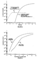
- FIG. 6 is a graph showing a plot of the measured charging current as a function of the floating gate voltage for both the prior art split gate device and the structure of the present invention.
- Curve a of FIG. 6 is a graph showing a plot of the charging current as a function of the floating gate voltage for the prior art split gate device and curve b of FIG. 6 shows a plot of the charging current as a function of the floating gate voltage for the structure of the present invention.
- Both devices used to obtain the data in FIG. 6 were fabricated on the same wafer using identical silicon processing. A comparison of the two curves demonstrates the improved results obtained by the structure of the present invention.
Landscapes
- Non-Volatile Memory (AREA)
Claims (5)
- Halbleiterstruktur für einen Langzeit-Permanentspeicher, die enthält:einen p-Bereich (12, 52) in einem Halbleitersubstrat (12, 50);einen n-Bereich (14, 54), der in dem p-Bereich (12, 52) liegt;ein Floating-Gate (18, 56), das aus einer über dem p-Bereich (12, 52) angeordneten Lage aus polykristallinem Silizium besteht und das eine Kante des n-Bereichs (14, 54) überlappt, wodurch ein Abschnitt des Floating-Gate (18, 56) über einem Teil des n-Bereichs (14, 54) liegt, wobei das Floating-Gate (18, 56) von der Oberfläche des Substrats (12, 50) durch eine Gateoxidlage (32) getrennt ist, wo das Floating-Gate (18, 56) über einem Teil des n-Bereichs (14, 54) liegt;eine Isolierlage auf dem Floating-Gate (18, 56); undeine Einrichtung (24, 28), die dem n-Bereich (14, 54) positives Potential bezogen auf den p-Bereich (12, 52) anlegt; wobei die Halbleiterstruktur weiterhin enthält:eine zweite Lage aus polykristallinem Silizium, die auf der Isolierlage angeordnet ist und einen ersten Bereich (20, 58), der einen Abschnitt des Floating-Gate (18, 56) überlagert und mit dem Floating-Gate durch eine erste Kapazität gekoppelt ist und einen zweiten Bereich (22, 60) separat vom ersten Bereich (20) hat, der einen anderen Abschnitt des Floating-Gate (18, 56) überlagert und mit dem Floating-Gate durch eine zweite Kapazität gekoppelt ist; undeine Einrichtung, die Minoritätselektronen in den p-Bereich (12, 52) bringt, wobeidas Floating-Gate (18, 56) dort, wo es nicht einen Teil des n-Bereichs (14, 54) überlagert, von der Oberfläche des Substrats (12, 50) durch eine Lage aus Feldoxid isoliert ist, unddie Feldoxidlage dicker ist als die Gateoxidlage (32) und weder der erste noch der zweite Bereich (20, 22 und 58, 60) über dem n-Bereich (14, 54) liegt.
- Halbleiterstruktur nach Anspruch 1, weiterhin dadurch gekennzeichnet, daßein weiterer n-Bereich (16) in dem p-Bereich (12) und beabstandet vom n-Bereich (14) angeordnet ist; undeine Einrichtung (26, 30) vorgesehen ist, die bezogen auf den p-Bereich (12), ein negatives Potential dem anderen n-Bereich (16) anlegt, um diesen in Durchlaßrichtung vorzuspannen und dadurch die Minoritätselektronen in den p-Bereich zu injizieren.
- Halbleiterstruktur nach Anspruch 1, die weiterhin dadurch gekennzeichnet ist, daßdas Halbleitersubstrat ein n-Halbleitersubstrat (50) und der p-Bereich ein p-Wannenbereich (52) ist und außerdem dadurch gekennzeichnet, daß:Mittel zum Anlegen eines bezüglich des n-Halbleitersubstrats (50) positiven Potentials an den p-Wannenbereich (52) vorgesehen sind, um den p-Wannenbereich in Durchlaßrichtung vorzuspannen und dadurch die Minoritätselektronen in den p-Bereich zu injizieren.
- Halbleiterstruktur nach Anspruch 1, weiterhin dadurch gekennzeichnet, daß
die Minoritätselektronen im p-Bereich (12) durch auf die Struktur fallendes sichtbares Licht oder Infrarotlicht erzeugt werden. - Halbleiterstruktur nach einem der Ansprüche 1 bis 4, weiterhin dadurch gekennzeichnet, daß
der erste Abschnitt (20, 58) des Floating-Gate (18, 56) größer als dessen zweiter Abschnitt (22, 60) und dadurch die erste Kapazität größer als die zweite Kapazität ist.
Applications Claiming Priority (3)
| Application Number | Priority Date | Filing Date | Title |
|---|---|---|---|
| US363678 | 1989-06-09 | ||
| US07/363,678 US4953928A (en) | 1989-06-09 | 1989-06-09 | MOS device for long-term learning |
| PCT/US1990/003001 WO1990015443A1 (en) | 1989-06-09 | 1990-06-05 | Mos device for long-term learning |
Publications (3)
| Publication Number | Publication Date |
|---|---|
| EP0429620A1 EP0429620A1 (de) | 1991-06-05 |
| EP0429620A4 EP0429620A4 (en) | 1991-09-04 |
| EP0429620B1 true EP0429620B1 (de) | 1997-09-03 |
Family
ID=23431230
Family Applications (1)
| Application Number | Title | Priority Date | Filing Date |
|---|---|---|---|
| EP90909501A Expired - Lifetime EP0429620B1 (de) | 1989-06-09 | 1990-06-05 | MOS-Anordnung für dauerhafte, nicht-flüchtige Speicherung |
Country Status (4)
| Country | Link |
|---|---|
| US (1) | US4953928A (de) |
| EP (1) | EP0429620B1 (de) |
| DE (1) | DE69031372D1 (de) |
| WO (1) | WO1990015443A1 (de) |
Families Citing this family (108)
| Publication number | Priority date | Publication date | Assignee | Title |
|---|---|---|---|---|
| US5101361A (en) * | 1989-09-29 | 1992-03-31 | The United States Of America As Represented By The Administrator Of The National Aeronautics And Space Administration | Analog hardware for delta-backpropagation neural networks |
| JPH04123471A (ja) * | 1990-09-14 | 1992-04-23 | Oki Electric Ind Co Ltd | 半導体記憶装置のデータ書込みおよび消去方法 |
| US5212541A (en) * | 1991-04-18 | 1993-05-18 | National Semiconductor Corporation | Contactless, 5v, high speed eprom/flash eprom array utilizing cells programmed using source side injection |
| US5243554A (en) * | 1991-05-09 | 1993-09-07 | Synaptics, Incorporated | Writable analog reference voltage storage device |
| US5166562A (en) * | 1991-05-09 | 1992-11-24 | Synaptics, Incorporated | Writable analog reference voltage storage device |
| US5541878A (en) * | 1991-05-09 | 1996-07-30 | Synaptics, Incorporated | Writable analog reference voltage storage device |
| US5303329A (en) * | 1991-12-10 | 1994-04-12 | Synaptics, Incorporated | Continuous synaptic weight update mechanism |
| US6965142B2 (en) * | 1995-03-07 | 2005-11-15 | Impinj, Inc. | Floating-gate semiconductor structures |
| US6144581A (en) * | 1996-07-24 | 2000-11-07 | California Institute Of Technology | pMOS EEPROM non-volatile data storage |
| US5875126A (en) * | 1995-09-29 | 1999-02-23 | California Institute Of Technology | Autozeroing floating gate amplifier |
| US5627392A (en) * | 1995-03-07 | 1997-05-06 | California Institute Of Technology | Semiconductor structure for long term learning |
| US5898613A (en) * | 1996-07-24 | 1999-04-27 | California Institute Of Technology | pMOS analog EEPROM cell |
| US5825063A (en) * | 1995-03-07 | 1998-10-20 | California Institute Of Technology | Three-terminal silicon synaptic device |
| US5990512A (en) * | 1995-03-07 | 1999-11-23 | California Institute Of Technology | Hole impact ionization mechanism of hot electron injection and four-terminal ρFET semiconductor structure for long-term learning |
| US5666307A (en) * | 1995-11-14 | 1997-09-09 | Programmable Microelectronics Corporation | PMOS flash memory cell capable of multi-level threshold voltage storage |
| DE19548529C1 (de) * | 1995-12-22 | 1997-04-03 | Siemens Ag | Verfahren zur Herstellung eines Neuron-MOS-Transistors auf der Basis eines CMOS-Prozesses |
| US5814853A (en) * | 1996-01-22 | 1998-09-29 | Advanced Micro Devices, Inc. | Sourceless floating gate memory device and method of storing data |
| DE19614010C2 (de) * | 1996-04-09 | 2002-09-19 | Infineon Technologies Ag | Halbleiterbauelement mit einstellbarer, auf einem tunnelstromgesteuerten Lawinendurchbruch basierender Stromverstärkung und Verfahren zu dessen Herstellung |
| JP2000515328A (ja) * | 1996-08-01 | 2000-11-14 | シーメンス アクチエンゲゼルシヤフト | メモリセル装置の作動方法 |
| US6026017A (en) * | 1997-04-11 | 2000-02-15 | Programmable Silicon Solutions | Compact nonvolatile memory |
| US8160864B1 (en) | 2000-10-26 | 2012-04-17 | Cypress Semiconductor Corporation | In-circuit emulator and pod synchronized boot |
| US8149048B1 (en) | 2000-10-26 | 2012-04-03 | Cypress Semiconductor Corporation | Apparatus and method for programmable power management in a programmable analog circuit block |
| US8103496B1 (en) | 2000-10-26 | 2012-01-24 | Cypress Semicondutor Corporation | Breakpoint control in an in-circuit emulation system |
| US7765095B1 (en) | 2000-10-26 | 2010-07-27 | Cypress Semiconductor Corporation | Conditional branching in an in-circuit emulation system |
| US8176296B2 (en) | 2000-10-26 | 2012-05-08 | Cypress Semiconductor Corporation | Programmable microcontroller architecture |
| US6724220B1 (en) | 2000-10-26 | 2004-04-20 | Cyress Semiconductor Corporation | Programmable microcontroller architecture (mixed analog/digital) |
| US6664909B1 (en) | 2001-08-13 | 2003-12-16 | Impinj, Inc. | Method and apparatus for trimming high-resolution digital-to-analog converter |
| US7406674B1 (en) | 2001-10-24 | 2008-07-29 | Cypress Semiconductor Corporation | Method and apparatus for generating microcontroller configuration information |
| US8078970B1 (en) | 2001-11-09 | 2011-12-13 | Cypress Semiconductor Corporation | Graphical user interface with user-selectable list-box |
| US8042093B1 (en) | 2001-11-15 | 2011-10-18 | Cypress Semiconductor Corporation | System providing automatic source code generation for personalization and parameterization of user modules |
| US6971004B1 (en) | 2001-11-19 | 2005-11-29 | Cypress Semiconductor Corp. | System and method of dynamically reconfiguring a programmable integrated circuit |
| US7774190B1 (en) | 2001-11-19 | 2010-08-10 | Cypress Semiconductor Corporation | Sleep and stall in an in-circuit emulation system |
| US8069405B1 (en) | 2001-11-19 | 2011-11-29 | Cypress Semiconductor Corporation | User interface for efficiently browsing an electronic document using data-driven tabs |
| US7844437B1 (en) | 2001-11-19 | 2010-11-30 | Cypress Semiconductor Corporation | System and method for performing next placements and pruning of disallowed placements for programming an integrated circuit |
| US7770113B1 (en) | 2001-11-19 | 2010-08-03 | Cypress Semiconductor Corporation | System and method for dynamically generating a configuration datasheet |
| US8103497B1 (en) | 2002-03-28 | 2012-01-24 | Cypress Semiconductor Corporation | External interface for event architecture |
| US7308608B1 (en) | 2002-05-01 | 2007-12-11 | Cypress Semiconductor Corporation | Reconfigurable testing system and method |
| US6958646B1 (en) | 2002-05-28 | 2005-10-25 | Impinj, Inc. | Autozeroing floating-gate amplifier |
| US7761845B1 (en) | 2002-09-09 | 2010-07-20 | Cypress Semiconductor Corporation | Method for parameterizing a user module |
| US20050030827A1 (en) * | 2002-09-16 | 2005-02-10 | Impinj, Inc., A Delaware Corporation | PMOS memory cell |
| US7212446B2 (en) * | 2002-09-16 | 2007-05-01 | Impinj, Inc. | Counteracting overtunneling in nonvolatile memory cells using charge extraction control |
| US7149118B2 (en) * | 2002-09-16 | 2006-12-12 | Impinj, Inc. | Method and apparatus for programming single-poly pFET-based nonvolatile memory cells |
| JP4189549B2 (ja) * | 2002-11-29 | 2008-12-03 | 独立行政法人科学技術振興機構 | 情報記憶素子及びその製造方法並びにメモリアレイ |
| US6867622B2 (en) * | 2003-01-07 | 2005-03-15 | Xicor, Inc. | Method and apparatus for dual conduction analog programming |
| US6898123B2 (en) * | 2003-01-07 | 2005-05-24 | Intersil Americas Inc. | Differential dual floating gate circuit and method for programming |
| US7113017B2 (en) * | 2004-07-01 | 2006-09-26 | Intersil Americas Inc. | Floating gate analog voltage level shift circuit and method for producing a voltage reference that operates on a low supply voltage |
| US6870764B2 (en) * | 2003-01-21 | 2005-03-22 | Xicor Corporation | Floating gate analog voltage feedback circuit |
| US6914812B2 (en) * | 2003-01-28 | 2005-07-05 | Intersil America Inc. | Tunnel device level shift circuit |
| US6847551B2 (en) * | 2003-01-28 | 2005-01-25 | Xicor, Inc. | Apparatus for feedback using a tunnel device |
| US6815983B2 (en) * | 2003-01-28 | 2004-11-09 | Xicor, Inc. | Analog floating gate voltage sense during dual conduction programming |
| US6894928B2 (en) * | 2003-01-28 | 2005-05-17 | Intersil Americas Inc. | Output voltage compensating circuit and method for a floating gate reference voltage generator |
| US6829164B2 (en) * | 2003-02-14 | 2004-12-07 | Xicor Corporation | Differential floating gate circuit and method for programming |
| US7429888B2 (en) * | 2004-01-05 | 2008-09-30 | Intersil Americas, Inc. | Temperature compensation for floating gate circuits |
| US7295049B1 (en) | 2004-03-25 | 2007-11-13 | Cypress Semiconductor Corporation | Method and circuit for rapid alignment of signals |
| US7283390B2 (en) | 2004-04-21 | 2007-10-16 | Impinj, Inc. | Hybrid non-volatile memory |
| US8111558B2 (en) * | 2004-05-05 | 2012-02-07 | Synopsys, Inc. | pFET nonvolatile memory |
| US8286125B2 (en) | 2004-08-13 | 2012-10-09 | Cypress Semiconductor Corporation | Model for a hardware device-independent method of defining embedded firmware for programmable systems |
| US8069436B2 (en) | 2004-08-13 | 2011-11-29 | Cypress Semiconductor Corporation | Providing hardware independence to automate code generation of processing device firmware |
| US7332976B1 (en) | 2005-02-04 | 2008-02-19 | Cypress Semiconductor Corporation | Poly-phase frequency synthesis oscillator |
| US7400183B1 (en) | 2005-05-05 | 2008-07-15 | Cypress Semiconductor Corporation | Voltage controlled oscillator delay cell and method |
| US8089461B2 (en) | 2005-06-23 | 2012-01-03 | Cypress Semiconductor Corporation | Touch wake for electronic devices |
| US8050876B2 (en) * | 2005-07-18 | 2011-11-01 | Analog Devices, Inc. | Automatic environmental compensation of capacitance based proximity sensors |
| US7307485B1 (en) | 2005-11-14 | 2007-12-11 | Cypress Semiconductor Corporation | Capacitance sensor using relaxation oscillators |
| US8085067B1 (en) | 2005-12-21 | 2011-12-27 | Cypress Semiconductor Corporation | Differential-to-single ended signal converter circuit and method |
| US7312616B2 (en) | 2006-01-20 | 2007-12-25 | Cypress Semiconductor Corporation | Successive approximate capacitance measurement circuit |
| US8067948B2 (en) | 2006-03-27 | 2011-11-29 | Cypress Semiconductor Corporation | Input/output multiplexer bus |
| US8144125B2 (en) | 2006-03-30 | 2012-03-27 | Cypress Semiconductor Corporation | Apparatus and method for reducing average scan rate to detect a conductive object on a sensing device |
| US8040142B1 (en) | 2006-03-31 | 2011-10-18 | Cypress Semiconductor Corporation | Touch detection techniques for capacitive touch sense systems |
| US7721609B2 (en) | 2006-03-31 | 2010-05-25 | Cypress Semiconductor Corporation | Method and apparatus for sensing the force with which a button is pressed |
| US8537121B2 (en) | 2006-05-26 | 2013-09-17 | Cypress Semiconductor Corporation | Multi-function slider in touchpad |
| US8089472B2 (en) | 2006-05-26 | 2012-01-03 | Cypress Semiconductor Corporation | Bidirectional slider with delete function |
| US8040321B2 (en) * | 2006-07-10 | 2011-10-18 | Cypress Semiconductor Corporation | Touch-sensor with shared capacitive sensors |
| US7253643B1 (en) | 2006-07-19 | 2007-08-07 | Cypress Semiconductor Corporation | Uninterrupted radial capacitive sense interface |
| US9507465B2 (en) | 2006-07-25 | 2016-11-29 | Cypress Semiconductor Corporation | Technique for increasing the sensitivity of capacitive sensor arrays |
| US8122307B1 (en) | 2006-08-15 | 2012-02-21 | Synopsys, Inc. | One time programmable memory test structures and methods |
| US9766738B1 (en) | 2006-08-23 | 2017-09-19 | Cypress Semiconductor Corporation | Position and usage based prioritization for capacitance sense interface |
| US8547114B2 (en) | 2006-11-14 | 2013-10-01 | Cypress Semiconductor Corporation | Capacitance to code converter with sigma-delta modulator |
| US8089288B1 (en) | 2006-11-16 | 2012-01-03 | Cypress Semiconductor Corporation | Charge accumulation capacitance sensor with linear transfer characteristic |
| US8058937B2 (en) * | 2007-01-30 | 2011-11-15 | Cypress Semiconductor Corporation | Setting a discharge rate and a charge rate of a relaxation oscillator circuit |
| US8516025B2 (en) | 2007-04-17 | 2013-08-20 | Cypress Semiconductor Corporation | Clock driven dynamic datapath chaining |
| US8026739B2 (en) | 2007-04-17 | 2011-09-27 | Cypress Semiconductor Corporation | System level interconnect with programmable switching |
| US7737724B2 (en) | 2007-04-17 | 2010-06-15 | Cypress Semiconductor Corporation | Universal digital block interconnection and channel routing |
| US9564902B2 (en) | 2007-04-17 | 2017-02-07 | Cypress Semiconductor Corporation | Dynamically configurable and re-configurable data path |
| US7827716B2 (en) * | 2007-04-17 | 2010-11-09 | Smith Marvin A | Mounting for sheet signage |
| US8130025B2 (en) | 2007-04-17 | 2012-03-06 | Cypress Semiconductor Corporation | Numerical band gap |
| US8040266B2 (en) | 2007-04-17 | 2011-10-18 | Cypress Semiconductor Corporation | Programmable sigma-delta analog-to-digital converter |
| US8092083B2 (en) | 2007-04-17 | 2012-01-10 | Cypress Semiconductor Corporation | Temperature sensor with digital bandgap |
| US8065653B1 (en) | 2007-04-25 | 2011-11-22 | Cypress Semiconductor Corporation | Configuration of programmable IC design elements |
| US9720805B1 (en) | 2007-04-25 | 2017-08-01 | Cypress Semiconductor Corporation | System and method for controlling a target device |
| US8266575B1 (en) | 2007-04-25 | 2012-09-11 | Cypress Semiconductor Corporation | Systems and methods for dynamically reconfiguring a programmable system on a chip |
| US8144126B2 (en) | 2007-05-07 | 2012-03-27 | Cypress Semiconductor Corporation | Reducing sleep current in a capacitance sensing system |
| US9500686B1 (en) | 2007-06-29 | 2016-11-22 | Cypress Semiconductor Corporation | Capacitance measurement system and methods |
| US8169238B1 (en) * | 2007-07-03 | 2012-05-01 | Cypress Semiconductor Corporation | Capacitance to frequency converter |
| US8570053B1 (en) | 2007-07-03 | 2013-10-29 | Cypress Semiconductor Corporation | Capacitive field sensor with sigma-delta modulator |
| WO2009006556A1 (en) | 2007-07-03 | 2009-01-08 | Cypress Semiconductor Corporation | Normalizing capacitive sensor array signals |
| US8089289B1 (en) | 2007-07-03 | 2012-01-03 | Cypress Semiconductor Corporation | Capacitive field sensor with sigma-delta modulator |
| US8049569B1 (en) | 2007-09-05 | 2011-11-01 | Cypress Semiconductor Corporation | Circuit and method for improving the accuracy of a crystal-less oscillator having dual-frequency modes |
| US8525798B2 (en) | 2008-01-28 | 2013-09-03 | Cypress Semiconductor Corporation | Touch sensing |
| US8487912B1 (en) | 2008-02-01 | 2013-07-16 | Cypress Semiconductor Corporation | Capacitive sense touch device with hysteresis threshold |
| US8358142B2 (en) | 2008-02-27 | 2013-01-22 | Cypress Semiconductor Corporation | Methods and circuits for measuring mutual and self capacitance |
| US8319505B1 (en) | 2008-10-24 | 2012-11-27 | Cypress Semiconductor Corporation | Methods and circuits for measuring mutual and self capacitance |
| US9104273B1 (en) | 2008-02-29 | 2015-08-11 | Cypress Semiconductor Corporation | Multi-touch sensing method |
| US7894261B1 (en) | 2008-05-22 | 2011-02-22 | Synopsys, Inc. | PFET nonvolatile memory |
| US8321174B1 (en) | 2008-09-26 | 2012-11-27 | Cypress Semiconductor Corporation | System and method to measure capacitance of capacitive sensor array |
| US8487639B1 (en) | 2008-11-21 | 2013-07-16 | Cypress Semiconductor Corporation | Receive demodulator for capacitive sensing |
| US8866500B2 (en) | 2009-03-26 | 2014-10-21 | Cypress Semiconductor Corporation | Multi-functional capacitance sensing circuit with a current conveyor |
| US9448964B2 (en) | 2009-05-04 | 2016-09-20 | Cypress Semiconductor Corporation | Autonomous control in a programmable system |
| US9268441B2 (en) | 2011-04-05 | 2016-02-23 | Parade Technologies, Ltd. | Active integrator for a capacitive sense array |
Citations (1)
| Publication number | Priority date | Publication date | Assignee | Title |
|---|---|---|---|---|
| US4622656A (en) * | 1982-12-16 | 1986-11-11 | Seiko Instruments & Electronics Ltd. | Non-volatile semiconductor memory |
Family Cites Families (5)
| Publication number | Priority date | Publication date | Assignee | Title |
|---|---|---|---|---|
| GB2073487B (en) * | 1980-04-07 | 1984-04-04 | Harari E | Semiconductor memory device |
| US4375087C1 (en) * | 1980-04-09 | 2002-01-01 | Hughes Aircraft Co | Electrically erasable programmable read-only memory |
| DE3174858D1 (en) * | 1980-12-25 | 1986-07-24 | Fujitsu Ltd | Nonvolatile semiconductor memory device |
| US4432075A (en) * | 1981-12-04 | 1984-02-14 | Hebrew University Of Jerusalem | Electrically programmable non-volatile memory |
| JPS5975671A (ja) * | 1982-10-25 | 1984-04-28 | Hitachi Ltd | 不揮発性半導体記憶装置 |
-
1989
- 1989-06-09 US US07/363,678 patent/US4953928A/en not_active Expired - Lifetime
-
1990
- 1990-06-05 WO PCT/US1990/003001 patent/WO1990015443A1/en not_active Ceased
- 1990-06-05 EP EP90909501A patent/EP0429620B1/de not_active Expired - Lifetime
- 1990-06-05 DE DE69031372T patent/DE69031372D1/de not_active Expired - Lifetime
Patent Citations (1)
| Publication number | Priority date | Publication date | Assignee | Title |
|---|---|---|---|---|
| US4622656A (en) * | 1982-12-16 | 1986-11-11 | Seiko Instruments & Electronics Ltd. | Non-volatile semiconductor memory |
Also Published As
| Publication number | Publication date |
|---|---|
| EP0429620A4 (en) | 1991-09-04 |
| DE69031372D1 (de) | 1997-10-09 |
| WO1990015443A1 (en) | 1990-12-13 |
| EP0429620A1 (de) | 1991-06-05 |
| US4953928A (en) | 1990-09-04 |
Similar Documents
| Publication | Publication Date | Title |
|---|---|---|
| US4953928A (en) | MOS device for long-term learning | |
| US5231299A (en) | Structure and fabrication method for EEPROM memory cell with selective channel implants | |
| US5242848A (en) | Self-aligned method of making a split gate single transistor non-volatile electrically alterable semiconductor memory device | |
| US5045488A (en) | Method of manufacturing a single transistor non-volatile, electrically alterable semiconductor memory device | |
| US5029130A (en) | Single transistor non-valatile electrically alterable semiconductor memory device | |
| KR100316086B1 (ko) | 신규한프로그래밍수단을갖는고밀도'전기적으로소거가능하고프로그램가능한판독전용메모리(eeprom)'셀어레이및이를제조하는방법 | |
| US5572054A (en) | Method of operating a single transistor non-volatile electrically alterable semiconductor memory device | |
| US5067108A (en) | Single transistor non-volatile electrically alterable semiconductor memory device with a re-crystallized floating gate | |
| JP2555027B2 (ja) | 半導体記憶装置 | |
| US5278087A (en) | Method of making a single transistor non-volatile electrically alterable semiconductor memory device with a re-crystallized floating gate | |
| US6388293B1 (en) | Nonvolatile memory cell, operating method of the same and nonvolatile memory array | |
| KR830001453B1 (ko) | 서브스트 레이트와 용량 결합된 부동 게이트의 earom기억 소자 | |
| US6804149B2 (en) | Nonvolatile memory cell, operating method of the same and nonvolatile memory array | |
| US4794565A (en) | Electrically programmable memory device employing source side injection | |
| US5424567A (en) | Protected programmable transistor with reduced parasitic capacitances and method of fabrication | |
| KR100316089B1 (ko) | 폴리터널스페이서를갖는완전특징고밀도"전기적으로소거가능하고프로그램가능한판독전용메모리(eeprom)"셀을제조하는방법 | |
| US5049956A (en) | Memory cell structure of semiconductor memory device | |
| EP0044384A2 (de) | Elektrisch veränderliche Festspeicherzelle | |
| EP1687826A2 (de) | Flash-speicher-programmierung durch verwendung von gate-induziertem sperrschichtleckstrom | |
| EP0579779B1 (de) | Elektrisch aenderbare einzel-transistor-halbleiterfestwertspeicheranordnung | |
| US4257056A (en) | Electrically erasable read only memory | |
| US6801456B1 (en) | Method for programming, erasing and reading a flash memory cell | |
| US5828099A (en) | Semiconductor device having a nonvolatile memory cell in which the floating gate is charged with hot charge carriers at the source side | |
| US5677876A (en) | Flash EEPROM with impurity diffused layer in channel area and process of production of same | |
| US7301197B2 (en) | Non-volatile nanocrystal memory transistors using low voltage impact ionization |
Legal Events
| Date | Code | Title | Description |
|---|---|---|---|
| PUAI | Public reference made under article 153(3) epc to a published international application that has entered the european phase |
Free format text: ORIGINAL CODE: 0009012 |
|
| 17P | Request for examination filed |
Effective date: 19910128 |
|
| AK | Designated contracting states |
Kind code of ref document: A1 Designated state(s): DE FR GB IT NL SE |
|
| A4 | Supplementary search report drawn up and despatched |
Effective date: 19910717 |
|
| AK | Designated contracting states |
Kind code of ref document: A4 Designated state(s): DE FR GB IT NL SE |
|
| 17Q | First examination report despatched |
Effective date: 19930907 |
|
| GRAG | Despatch of communication of intention to grant |
Free format text: ORIGINAL CODE: EPIDOS AGRA |
|
| GRAH | Despatch of communication of intention to grant a patent |
Free format text: ORIGINAL CODE: EPIDOS IGRA |
|
| GRAH | Despatch of communication of intention to grant a patent |
Free format text: ORIGINAL CODE: EPIDOS IGRA |
|
| RAP1 | Party data changed (applicant data changed or rights of an application transferred) |
Owner name: SYNAPTICS, INCORPORATED |
|
| GRAA | (expected) grant |
Free format text: ORIGINAL CODE: 0009210 |
|
| AK | Designated contracting states |
Kind code of ref document: B1 Designated state(s): DE FR GB IT NL SE |
|
| PG25 | Lapsed in a contracting state [announced via postgrant information from national office to epo] |
Ref country code: IT Free format text: LAPSE BECAUSE OF FAILURE TO SUBMIT A TRANSLATION OF THE DESCRIPTION OR TO PAY THE FEE WITHIN THE PRE;WARNING: LAPSES OF ITALIAN PATENTS WITH EFFECTIVE DATE BEFORE 2007 MAY HAVE OCCURRED AT ANY TIME BEFORE 2007. THE CORRECT EFFECTIVE DATE MAY BE DIFFERENT FROM THE ONE RECORDED.SCRIBED TIME-LIMIT Effective date: 19970903 Ref country code: FR Free format text: LAPSE BECAUSE OF FAILURE TO SUBMIT A TRANSLATION OF THE DESCRIPTION OR TO PAY THE FEE WITHIN THE PRESCRIBED TIME-LIMIT Effective date: 19970903 Ref country code: NL Free format text: LAPSE BECAUSE OF FAILURE TO SUBMIT A TRANSLATION OF THE DESCRIPTION OR TO PAY THE FEE WITHIN THE PRESCRIBED TIME-LIMIT Effective date: 19970903 |
|
| REF | Corresponds to: |
Ref document number: 69031372 Country of ref document: DE Date of ref document: 19971009 |
|
| PG25 | Lapsed in a contracting state [announced via postgrant information from national office to epo] |
Ref country code: SE Effective date: 19971203 |
|
| PG25 | Lapsed in a contracting state [announced via postgrant information from national office to epo] |
Ref country code: DE Effective date: 19971204 |
|
| EN | Fr: translation not filed | ||
| NLV1 | Nl: lapsed or annulled due to failure to fulfill the requirements of art. 29p and 29m of the patents act | ||
| PLBE | No opposition filed within time limit |
Free format text: ORIGINAL CODE: 0009261 |
|
| STAA | Information on the status of an ep patent application or granted ep patent |
Free format text: STATUS: NO OPPOSITION FILED WITHIN TIME LIMIT |
|
| 26N | No opposition filed | ||
| REG | Reference to a national code |
Ref country code: GB Ref legal event code: IF02 |
|
| PGFP | Annual fee paid to national office [announced via postgrant information from national office to epo] |
Ref country code: GB Payment date: 20020529 Year of fee payment: 13 |
|
| PG25 | Lapsed in a contracting state [announced via postgrant information from national office to epo] |
Ref country code: GB Free format text: LAPSE BECAUSE OF NON-PAYMENT OF DUE FEES Effective date: 20030605 |
|
| GBPC | Gb: european patent ceased through non-payment of renewal fee |
Effective date: 20030605 |