EP0426331B1 - Dispositif et procédé de commande d'interruption programmable - Google Patents
Dispositif et procédé de commande d'interruption programmable Download PDFInfo
- Publication number
- EP0426331B1 EP0426331B1 EP90311376A EP90311376A EP0426331B1 EP 0426331 B1 EP0426331 B1 EP 0426331B1 EP 90311376 A EP90311376 A EP 90311376A EP 90311376 A EP90311376 A EP 90311376A EP 0426331 B1 EP0426331 B1 EP 0426331B1
- Authority
- EP
- European Patent Office
- Prior art keywords
- interrupt
- interrupt request
- edge
- triggered
- bit
- Prior art date
- Legal status (The legal status is an assumption and is not a legal conclusion. Google has not performed a legal analysis and makes no representation as to the accuracy of the status listed.)
- Expired - Lifetime
Links
Images


Classifications
-
- G—PHYSICS
- G06—COMPUTING OR CALCULATING; COUNTING
- G06F—ELECTRIC DIGITAL DATA PROCESSING
- G06F13/00—Interconnection of, or transfer of information or other signals between, memories, input/output devices or central processing units
- G06F13/14—Handling requests for interconnection or transfer
- G06F13/20—Handling requests for interconnection or transfer for access to input/output bus
- G06F13/24—Handling requests for interconnection or transfer for access to input/output bus using interrupt
- G06F13/26—Handling requests for interconnection or transfer for access to input/output bus using interrupt with priority control
Definitions
- the present invention generally relates to a programmable interrupt controller for a computer system and, more particularly, to an interrupt controller having a plurality of interrupt request inputs, each of which may be programmed to detect either edge-triggered or level-triggered interrupt requests on a per input basis.
- a computer system typically includes a central processing unit (CPU) connected to a system bus having data, address, and control lines.
- the bus is connected to other computer system components, such as program memory, and also to peripheral devices via a suitable interface.
- the interface may include interface devices for translating voltages or signal formats for compatibility between the computer system and the peripheral devices. Suitable interface connectors are often employed.
- Communication between the CPU and the peripheral devices can include sensory or command information.
- a peripheral device acting as a sensor may produce data signals indicative of parameters the peripheral sensing device is sensing, such as temperature, voltage, or other parameters.
- the data signals may be translated to a suitable form and read through the interface by the CPU to provide the CPU with needed data regarding the sensed parameters.
- the peripheral devices may be controllers.
- the CPU commands a peripheral controlling device by writing suitable commands through the interface to the peripheral controlling device. The device then takes suitable action in accordance with the command.
- a first scheme is called polling.
- the CPU executes a polling routine at intervals of time. Typically, a hardware timer will cause the CPU to execute the polling routine periodically.
- the CPU reads information from the peripheral devices indicating whether the status of a sensed parameter has changed or whether there is a need to send a command to the peripheral device.
- the CPU takes appropriate action, such as sending commands to the peripheral device or updating a record of the status of the peripheral device stored in computer system memory.
- Polling is commonly used in computer systems which interface with a large number of peripheral devices.
- polling has the disadvantage that the polling routine must be executed frequently, thereby consuming a large amount of CPU processing time.
- the status information read from the peripheral devices indicates that no action is necessary.
- the time spent executing the polling routine in retrospect proves to be unproductive. In computer system involving a great deal of activity or real-time applications, the time spent repeating the polling routine can reduce processing efficiency.
- an interface between a CPU and a peripheral device can include circuitry which detects a change of status in the peripheral device for which service is required and provides a suitable interrupt request signal to the CPU.
- An interrupt driven system of this type provides improved processing efficiency since interrupt routines are executed only when required. However, frequently a CPU will be employed to service a plurality of peripheral devices. In such a system, questions arise as to how to go about determining which peripheral device needs to be serviced in response to an interrupt request. Also, if several peripheral devices simultaneously provide interrupt request signals, there must be a way of determining which one is serviced first. In order to provide practical answers to these questions, programmable interrupt controllers have been designed and utilized in conjunction with computer systems. An interrupt controller typically has a single interrupt request output which is connected to the interrupt request input of the CPU. The interrupt controller also has a plurality of interrupt request inputs. Each interrupt request input in connected to a peripheral device. Thus, when the peripheral device requires servicing, it produces a suitable interrupt request signal which is received by the interrupt controller. The interrupt controller then interrupts the CPU and causes a suitable interrupt service routine to be executed.
- a well known example of an interrupt controller is the 8259A programmable interrupt controller manufactured by Intel Corporation.
- the 8259A is designed to operate with two different types of microprocessors which support multiple interrupt request inputs in two different ways.
- the first type is exemplified by the Intel 8080/8085 microprocessors which service interrupt requests by executing a software instruction for calling a subroutine which has as an operand an address of a subroutine.
- the second type is exemplified by the Intel 8086 microprocessor which services interrupt requests by using an 8-bit vector to select an interrupt service routine address from a table of addresses stored in a contiguous page of memory.
- the 8259A will interrupt the CPU and provide either a subroutine call instruction followed by an interrupt service routine address or an eight bit interrupt vector over the system bus to the CPU.
- the 8259A provides the CPU with information as to which interrupt service routine to execute, thereby ensuring that the CPU services the peripheral device which requested the interrupt in a suitable manner.
- the 8259A may be configured to detect interrupt requests on its interrupt request inputs as either low-to-high voltage transitions or as high voltage levels.
- the 8259A interrupt request inputs can be configured as either edge- triggered or level-triggered.
- Many peripheral devices have been designed to produce edge-triggered interrupt request signals in the form of low-to-high voltage transitions.
- an edge-triggered interrupt request is a transition from a recognizably low voltage to a recognizably high voltage within a predetermined time limit.
- peripheral devices which request service by means of high voltage levels are becoming more common. It is desirable for an interrupt controller to be able to detect level-triggered interrupts to allow for the use of peripheral devices which produce level-triggered interrupt requests, thereby providing for greater flexibility in interface design. It is desirable for a computer system including an interrupt controller to be flexible enough to accommodate the newer peripheral devices producing level-triggered interrupt requests while remaining backward compatible with older peripheral devices which produce edge-triggered interrupt requests.
- EP-A-0 358 330 which is cited as prior art in accordance with Article 54(3) of the European Patent Convention, describes an interrupt controller, for a computer system having a central processing unit (CPU), the controller comprising: a plurality of inputs connected to receive interrupt requests from a plurality of peripheral devices; means (66) for sending an interrupt signal to the CPU over an interrupt request output in response to any one of the interrupt requests; a priority resolver for assigning to each input in the plurality of inputs a priority position to create a hierarchy for the purpose of resolving which interrupt request is first serviced when time overlapping interrupt requests are received; and, means for independently establishing each input to be responsive to either edge-triggered or level-triggered interrupt requests; the means for establishing comprising a first initialization command register having a plurality of bits, each bit respectively corresponding to one of the inputs, and wherein each input is established to be responsive to edge-triggered interrupt requests when the respective bit is in a first state and each input is established to be responsive to level-triggered interrupt requests when the respective
- An aim of the present invention is to provide a programmable interrupt controller which detects edge-triggered and level-triggered interrupt requests from peripheral devices on a per peripheral device basis.
- an interrupt controller for a computer system having a central processing unit (CPU), the controller comprising: a plurality of inputs connected to receive interrupt requests from a plurality of peripheral devices; means for sending an interrupt signal to the CPU over an interrupt request output in response to any one of the interrupt requests; a priority resolver for assigning to each input in the plurality of inputs a priority position to create a hierarchy for the purpose of resolving which interrupt request is first serviced when time overlapping interrupt requests are received; and, means for independently establishing each input to be responsive to either edge-triggered or level-triggered interrupt requests; the means for establishing comprising a first initialization command register having a plurality of bits, each bit respectively corresponding to one of the inputs, and wherein each input is established to be responsive to edge-triggered interrupt requests when the respective bit is in a first state and each input is established to be responsive to level-triggered interrupt requests when the respective bit is in a second state; the interrupt controller being characterised in that the means for establishing comprises an
- peripheral devices utilizing either edge-triggered or level-triggered interrupt requests may be used on the various interrupt request inputs.
- peripheral devices are interchangeable. Replacing an edge-triggered peripheral device with a level-triggered peripheral device merely requires changing the programming configuration of the interrupt controller.
- a computer system may be upgraded with new level-triggered peripheral devices without incurring undesirably high costs for replacing otherwise functional peripheral devices.
- a method for receiving and servicing an edge-triggered interrupt request from a first source and a level-triggered interrupt request from a second source comprising the steps of programming an interrupt controller having first and second interrupt request inputs to detect edge-triggered interrupt requests incoming over the first interrupt request input and to detect level-triggered interrupt requests incoming over the second interrupt request input, said programming being done on a per input basis, detecting and latching an edge-triggered interrupt request incoming over the first input, interrupting the CPU to cause the CPU to service the edge-triggered interrupt request, detecting a level-triggered interrupt request incoming over the second input, interrupting the CPU to cause the CPU to service the level-triggered interrupt request, loading the latched edge-triggered interrupt request into a first bit of an interrupt request register corresponding to the first interrupt request input, and loading the level-triggered interrupt request into a second bit of the interrupt request register corresponding to the second interrupt request input.
- a computer system comprising: a central processing unit (CPU) having a program including a plurality of interrupt service routines; a group of peripheral devices including at least first and second peripheral devices having edge-triggered and level-triggered interrupt requests, respectively; a bus connected to the CPU; an interrupt controller according to the invention connected between the group of peripheral devices and the bus for interrupting the CPU responsive to the edge-triggered and level-triggered interrupt requests from the group of peripherals and causing the CPU to execute the interrupt service routines, thereby servicing the interrupt requests.
- CPU central processing unit
- a group of peripheral devices including at least first and second peripheral devices having edge-triggered and level-triggered interrupt requests, respectively
- a bus connected to the CPU
- an interrupt controller according to the invention connected between the group of peripheral devices and the bus for interrupting the CPU responsive to the edge-triggered and level-triggered interrupt requests from the group of peripherals and causing the CPU to execute the interrupt service routines, thereby servicing the interrupt requests.
- an interrupt controller for a computer system which allows for the peripheral devices in the group to be replaced or upgraded in a manner which may include changing the mix of edge-triggered and level-triggered interrupt requests while preserving the system's ability to service the peripheral devices.
- the interrupt controller is capable of servicing interrupt requests from any particular mix of peripheral devices having edge- triggered and level-triggered interrupt requests without regard to the address location of each device.
- each peripheral can have either edge-triggered or level-triggered interrupt requests, and the interrupt controller accommodates edge-triggered and level-triggered interrupts on a per interrupt line basis.
- a computer system having a programmable interrupt controller which may be programmed in accordance with currently existing software written for previously existing programmable interrupt controllers. If the controller is so programmed, all inputs shall detect either edge- triggered interrupt requests or level-triggered interrupt requests so that a controller in accordance with the invention operates in a manner consistent with such previously existing programmable interrupt controllers. Thus, the controller is backward compatible with existing computer systems.
- the programmable interrupt controller of the present invention thus provides a method for receiving and servicing edge-triggered and level-triggered interrupts.
- Figure 1 is a block diagram of a computer system utilizing an interrupt controller in accordance with the invention for servicing peripheral devices.
- FIG. 2 is a block diagram of an interrupt controller in accordance with the invention.
- Figure 3 is a logic diagram showing a hardware configuration of initialization control word registers utilized in a preferred embodiment of the invention.
- Figures 4-6 are detailed logic diagrams of various initialization control word registers shown in Figure 3.
- FIG 7 is a detailed logic diagram showing a stage of the interrupt request register (IRR) shown in Figure 2.
- IRR interrupt request register
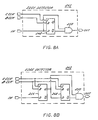
- Figures 8A and 8B are first and second embodiments, respectively, of the edge detector shown in Figure 7.
- Figures 9A-9E are tables showing how the initialization control word registers of the preferred embodiment of the programmable interrupt controller may be programmed for various system configurations.
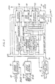
- a computer system bus 2 is connected to a central processing unit (CPU) 4, memory 6, an interrupt controller 8 , and a plurality of interfaces 10-24.
- the interfaces 10-24 may be any type of suitable shared boundary and may include electronic interface devices, such as universal asynchronous receivers/transmitters (UARTS) and suitable connectors.
- the interfaces 10-24 are connected to peripheral devices 26-40 which may be sensing or monitoring devices, such as thermocouples or voltage sensors, or control devices, such as motors, electronic switches, or other devices, suitable for computer controlled applications.
- the peripheral devices 26-40 have interrupt request outputs which are connected via lines 42-56 to interrupt request inputs on the interrupt controller 8.
- the interrupt controller 8 includes an interrupt request output connected via a line 58 to an interrupt request input on the CPU 4.
- An interrupt acknowledge line 60 is connected to carry an interrupt acknowledge signal from the CPU 4 back to the interrupt controller 8.
- the lines 58, 60 are treated as part of a system bus including data, address, and control lines.
- Figure 1 shows the interrupt request line 58 and the interrupt acknowledge line 60 running between the interrupt controller 8 and the CPU 4 as separate lines.
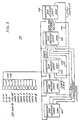
- FIG. 2 shows a more detailed diagram of the interrupt controller 8.
- a data bus buffer 62 provides an interface between the system data bus 2 ( Figure 1) and an internal data bus 64.
- An interrupt request register (IRR) 66 is connected to the data bus 64 and has eight interrupt request inputs collectively shown as 68.
- the interrupt request inputs 68 are individually designated IRQ 0 -IRQ 7
- the IRR 66 has an interrupt request output INTR 70 which is connected to the line 58 shown in Figure 1.
- the embodiment depicted in Figure 2 includes an interrupt acknowledge input INTA 72 connected to the interrupt acknowledge line 60 from the CPU 4.
- a read/write control module 74 is provided having read and write inputs (IOR, IOW) 76, 78, a chip select input (CS) 80, and an address select input (AO) 82.
- IOR, IOW read and write inputs
- CS chip select input
- AO address select input
- a cascade control 84 is provided having a three bit cascade bus (CAS) 86 which is an output when the controller is used as a master and an input when the controller is used as a slave.
- CAS cascade bus
- ISR interrupt service register
- the ISR 88 stores a bit corresponding to each interrupt request input 68. Bits in the ISR 88 are set to indicate which interrupt levels are being serviced.
- the IRR 66 generates an interrupt request which is delivered to the CPU 4 over the interrupt request line 70. An acknowledgement from the CPU 4 is received over the interrupt acknowledge line 72 by the IRR 66, the ISR 88, a vector generator 90, and a priority resolver 92, all of conventional design.
- the interrupt controller 8 also includes a series of initialization command word (ICW) registers, collectively shown as 94, which are written into by the CPU 4 through the data bus buffer 62 and the internal data bus 64 upon initialization.
- ICW registers 94 provide vector bits to the vector generator 90 which, in turn, presents a suitable interrupt vector or service routine address onto the internal data bus 64.
- the priority resolver 92 assigns each of the interrupt request inputs (IRQ 0 -IRQ 7 ) 68 a priority position with respect to the other inputs 68 to create a hierarchy for resolving which interrupt request is serviced first when simultaneous or time overlapping interrupt requests are received by the IRR 66. Any suitable priority scheme may be used.
- priority may be fixed in a given order.
- priority may rotate, i.e., an input may go to the bottom of the priority hierarchy after it has been serviced.
- operation command word (OCW) registers OCW1, OCW2, and OCW3 cause the interrupt controller 8 to operate in various modes in a well known manner.
- OCW1 is stored in a mask register 96.
- the bits of the OCW1 register serve to mask selected ones of the IRQ inputs 68.
- OCW2 and OCW3 are stored in an operation register 98 and provide other operational modes.
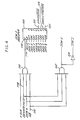
- the ICW registers 94 are depicted in more detail in Figure 3.
- the registers include ICW1 (shown as 100), ICW2 (shown as 102), ICW3 (shown as 104), ICW4 (shown as 106, and ICW5 (shown as 108).
- the ICW registers 94 are shown in block diagram along with certain interconnections. Still more detailed drawings, including additional logic used to interconnect the registers, are provided and discussed below. While the following discussion illustrates a preferred embodiment in terms of various functions controlled by bits in these registers, it is to be understood that an interrupt controller in accordance with the invention may include varying numbers of registers and may make bit assignments for functions, such as those described below, in arrangements different from the present embodiment.
- the ICW registers 94 are programmed during initialization by the CPU 4 which writes values into the registers to set bits so as to configure the interrupt controller 8 in a desired fashion. Examples of ICW programming for various configurations are shown in Figures 9A-9E and the related text. In the present embodiment, the ICW registers 94 are written into in sequence. Alternatively, the ICW registers 94 could be separately addressable for reading and writing in any desired sequence. Each register produces a signal indicating that it has been written into. In Figure 3, these signals are indicated as ICW1/ICW1, COMPL ICW2, COMPL ICW3, COMPL ICW4 AND ICW5 COMPLETE. These signals are used to enable writing into the subsequent registers. While all of the ICW 94 registers are used for completely configuring the interrupt controller 8, certain registers contain bits which are particularly relevant to the disclosed embodiment. These registers are described in more detail below.
- Figure 3 may be taken as a summary of the more detailed subject matter appearing below.
- the architecture of the preferred embodiment as depicted in Figure 3 is similar in many respects to the Intel 8259A programmable interrupt controller referred to above.
- the ICW1, ICW2, ICW3, and ICW4 registers 100, 102, 104, 106 are substantially similar to comparable registers in the 8259A. Points of distinction between these registers as used in the 8259A and in the present preferred embodiment are noted below.
- an objective of the present invention is to provide a programmable interrupt controller in which a plurality of interrupt request inputs may be programmed to be either edge-sensitive or level-sensitive on a per interrupt basis
- the ICW5 register 108 includes a bit corresponding to each interrupt request input. Each bit may be programmed in one of two states, the two states corresponding respectively to edge-sensitivity and level-sensitivity.
- a user may program an interrupt controller as depicted in Figure 3 to provide the desired per interrupt selectability of edge-triggering or level-triggering.
- a programmable interrupt controller in accordance with the invention need not follow this exact architecture. Different types of interrupt controllers will have different types of programming characteristics. It may be that configuration parameters in other interrupt controllers may be programmed in a manner other than through the use of control registers. Also, similar configuration parameters may be defined in terms of different programmable bits from those described below in conjunction with the initialization control registers. However, in any such programmable interrupt controller according to the present invention, a plurality of interrupt request inputs may be programmed on a per interrupt basis for edge-sensitivity or level-sensitivity, either through the use of a register such as the ICW5 register 108 or through other suitable means.
- backward compatibility with the Intel 8259A is provided by using a LEVEL/EDGE bit. While the 8259A uses this single bit to program all interrupt request inputs to be either edge-sensitive or level-sensitive, the present preferred embodiment uses this same bit to select either edge-sensitivity for all interrupt request inputs or selectability on a per interrupt basis through the use of the bits in the ICW5 register 108. This use of the LEVEL/EDGE bit in this manner is an additional novel feature of the present invention. While it is defined in the present preferred embodiment to provide backward compatibility with the Intel 8259A, other programmable interrupt controllers might provide backward compatibility with previously existing interrupt controllers in an essentially analogous manner by adapting the definition of their own configuration parameters in a suitable fashion.
- Figure 3 shows various system signals which are provided to all of the initialization command word registers. These signals are all essentially conventional in nature. They are standard computer system data, address, and control bus signais.
- the lines DATA0-DATA7 are data bus lines. They are individual lines which together make up the eight bit data bus 64 shown in Figure 2.
- the line A0 is the least significant bit of a conventional address bus.
- Many large scale integrated circuits, such as interface devices and interrupt controllers may be programmed through the use of memory-mapped input/output. This is a conventional programming technique in which one or more memory addresses are used to program a peripheral device, such as an interface device or an interrupt controller.
- system address bus lines may be connected in hardware to these inputs to provide addressability through software programming.
- the signals I/O WRITE PULSE, CCLK, and BCLK are conventional control signals.
- the present preferred embodiment utilizes two separate clock signal CCLK and BCLK.
- a plurality of clock signals may be used if they have a given phase relationship between each other.
- a single clock may be used.
- FIG. 4 a more detailed drawing is provided showing the ICW1 register 100 and logic utilized for writing into it.
- Writing into the ICW1 register 100 is facilitated by means of the system clocks BCLK and CCLK.
- An AND gate 110 is provided for enabling the system CCLK to reach a C input 112 of the ICW1 register 100 under suitable conditions.
- a B input 114 of the ICW1 register 100 is connected directly to the system BCLK.
- an address line 116 must be high as well as an I/O WRITE PULSE 118.
- DATA4 is also connected to the AND gate 110.
- Data bits on the data bus 64 are written into the ICW1 register 100 in a conventional fashion to provide various defined signals representing a desired configuration of the interrupt controller.
- the Bit 3 of the ICW1 register is the LEVEL/EDGE bit 120.
- a corresponding bit defines whether all of the interrupt request inputs were level-sensitive or edge-sensitive.
- the function of the LEVEL/EDGE bit 120 has been modified to provide backward compatibility with the 8259A as well as selectability on a per interrupt basis in accordance with the invention. When the LEVEL/EDGE bit 120 is low, all interrupt request inputs are edge-sensitive.
- interrupt request inputs are programmable on a per interrupt basis to be either edge-sensitive or level-sensitive. Exactly how each interrupt request input is programmed for detecting interrupt requests in described below in conjunction with the ICW5 register 108. Defining bit 3 of the ICW1 register 100 in this manner is a practical manner for implementing the invention while also providing backward compatibility. Since many older systems employing the 8259A use peripheral devices producing edge-triggered interrupt requests, system software for configuring the 8259A would typically program bit 3 of the ICW1 register 100 to be low for edge-triggering. Thus, an interrupt controller in accordance with the invention programming this bit to be low would operate in the same manner as an 8259A. On the other hand, newer systems employing newer level-triggered peripheral devices and an interrupt controller in accordance with the invention could easily program the LEVEL/EDGE bit 120 high, thereby providing interrupt selectability on a per interrupt basis.
- the LEVEL/EDGE bit 120 could be implemented such that the high value would configure all interrupt request inputs to be level-sensitive and a low value would permit per input selectability.
- the LEVEL/EDGE bit 120 could be ignored and each interrupt request input would always be configured in accordance with a corresponding bit in ICW5 as described below.
- the state of the LEVEL/EDGE bit 120 could be reversed, i.e., a high state could correspond with edge-sensitive interrupt requests. Then it would be an EDGE/LEVEL bit.
- Bit O of the ICW1 register is an IC4 bit 122
- this bit is a 1
- the ICW4 register 106 is programmed and its bits define interrupt controller parameters as discussed in conjunction with Figure 5 and tabulated in Figures 9A-9E.
- the ICW4 register 106 is not programmed and the parameters are set to default values as described in conjunction with Figure 9E which illustrates a case in which the IC4 bit 122 is low.
- Figure 4 also shows bit 1 of the ICW1 register 100 which is a SINGLE/CASCADE bit 124.
- This bit is utilized in a conventional manner when a plurality of interrupt controllers are used in a system.
- a master interrupt controller can be used with up to eight slave controllers, thereby permitting up to sixty-four interrupt request inputs at up to sixty-four priority levels to be handled.
- the cascade control 84 has a three-bit cascade bus 86.
- the cascade mode is selected by programming the SINGLE/CASCADE bit 124 low and the controller is configured as a master (as will be described later in conjunction with the ICW4 register 106), then the three lines making up the cascade bus 86 are outputs which are used to select one of up to eight slave controllers.
- an AND gate 126 and an inverter 128 which produce high-true and low-true versions of a signal ICW1.
- the AND gate 126 has inputs connected to receive the system I/O WRITE PULSE 118 as well as the address line 116 and the DATA4, the fourth bit of the data bus 64. Accordingly, the AND gate 126 outputs the signal ICW1 as a pulse synchronized with the I/O WRITE PULSE 118 when the ICW1 register 100 is written into.
- This signal ICW1 is used for clearing the remaining ICW registers when the programming sequence, beginning with the ICW1 register 100, commences, thereby enabling programming of the other registers in sequence.
- the ICW4 register 106 is clocked by means of the system BCLK and the system CCLK as enabled by an enabling logic network. Since, in accordance with the preferred embodiment, the ICW2 and/or ICW3 registers 102, 104 must be written as a prerequisite to writing the ICW4 register 106, the enabling logic network receives signals indicating the completion of writing into the registers 102, 104. The signals are called COMPL ICW2 and COMPL ICW3 and are shown in Figure 3 as 130 and 132, respectively. Because they are of conventional configuration, the ICW2 and ICW3 registers 102, 104 have not been disclosed in detail in the present specification.
- the network includes an AND gate 134 connected to receive as inputs a signal COMPL ICW2 (indicating that the ICW2 register 102 has been programmed) and the SINGLE/CASCADE bit 124 of the ICW1 register 100.
- An OR gate 136 is connected to receive as inputs the output of the AND gate 134 and a signal COMPL ICW3, indicating that the ICW3 register 104 has been programmed. As shown in Figure 13 and discussed hereinafter, in the single mode, the ICW3 register 104 is not programmed. Thus, programming the ICW4 register 106 may be enabled either by the completion of programming of the ICW3 register 104 or, in the single mode, by that of the ICW2 register 102.
- the output of the OR gate 136 is connected to an input of an AND gate 138.
- the AND gate 138 produces an output which enables the system CCLK through an AND gate 140 to the ICW4 register 106 when all necessary prerequisites are met.
- An output from the OR gate 136 is one prerequisite.
- the I/O WRITE PULSE 118 and the address line AO 116 are prerequisites for enabling the CCLK to the ICW4 register 106.
- bits 5, 6, and 7 of the data bus 64, which are not used in the ICW4 register 106, must be low. These three data bits are shown as inverted in a conventional manner to accommodate the active high inputs of the AND gate 138.
- Circuitry is also provided in Figure 5 for enabling the programmable interrupt controller 8 upon completion of programming of all of the ICW registers.
- the controller 8 is enabled when the ICW5 register 108 has been programmed if the LEVEL/EDGE bit 120 is high.
- the ICW5 register 108 is programmed to select edge-triggering or level-triggering on a per interrupt basis. If the LEVEL/EDGE bit 120 has been programmed low, all interrupt request inputs default to edge-sensitivity. Accordingly, an AND gate 142 is provided to enable the programmable interrupt controller 8 when the LEVEL/EDGE bit 120 is high and the ICW5 register 108 has been programmed, as indicated by an ICW5 COMPLETE signal 144.
- a set/reset latch 146 is provided to indicate that the ICW4 register 106 has been written into by producing a signal COMPL ICW4, shown as 148.
- the output of the latch 146 is also used to indicate that programming of the interrupt controller 8 is completed. Where the LEVEL/EDGE bit 120 is low, indicating that the interrupt controller 8 defaults to a situation where all inputs are edge-sensitive, there is no need to program the ICW5 register 108. Accordingly, the interrupt controller 8 is ready to be enabled after the ICW4 register 106 has been programmed.
- the LEVEL/EDGE bit 120 is inverted by an inverter 150 to indicate edge-triggering when high.
- a high true output 152 of the latch 146 is connected along with the inverted LEVEL/EDGE bit 120 to an AND gate 154.
- Outputs of the AND gates 142 and 154 are connected to inputs of an OR gate 156.
- the output of the OR gate 156 is a PIC ENABLE signal 158 which, when high, indicates that the programmable interrupt controller 8 is enabled.
- PIC ENABLE 158 is inverted by an inverter 160 to produce a PICENABLE signal 162 which is used where an active low signal indicating that the programmable interrupt controller is enabled is required.
- the latch 146 is clocked by the system CCLK and BCLK.
- a low value is clocked into the latch 146.
- a low-true output 164 of the latch 146 will be high, enabling the AND gate 138 which receives the ICW4 decoding signals.
- an OR gate 166 goes high, raising a first input 168 of an AND gate 170, the output of which is connected to a data input 172 of the latch 146.
- a second input 174 of the AND gate 170 is connected to ICW1.
- ICW1 is normally high and goes low only at the time when the ICW1 register 100 is written into, thereby initiating the programming of the ICW registers. Accordingly, at the moment when the ICW1 signal goes low, a low value is clocked into the latch 146.
- the low-true output 164 of the latch 146 is high, enabling the AND gate 138.
- the high-true output 152 of the latch 146 goes low, so the OR gate 166 remains low until the output of the AND gate 138 goes high.
- the latch 146 is finally set at the time when the ICW4 register 106 is written since the output of the AND gate 138 goes high, enabling the CCLK through the AND gate 140 to the C input of the ICW4 register 106 and also raising the output of the OR gate 166, thereby raising the output of the AND gate 170 connected to the data input 172 of the latch 146.
- the PIC ENABLE signal 158 goes high at the time when the latch 146 is set as the ICW4 register 106 is being written into.
- a microprocessor mode (uPM) bit 176 is set according to which type of microprocessor the interrupt controller is working with. If the uPM bit 176 is low, the interrupter controller 8 will operate in accordance with an 8080 or 8085 microprocessor by providing a sixteen bit interrupt service routine address.
- a MASTER/SLAVE (M/S) bit 178 defines whether the interrupt controller 8 is a master or slave. This bit is used in the cascade mode in which interrupt request outputs of slave controllers are connected to interrupt request inputs of a master controller.
- An automatic end of interrupt (AEOI) bit 180 may be programmed high to cause the programmable interrupt controller 8 to automatically perform a non-specific end of interrupt operation following the last interrupt acknowledge pulse received over the interrupt acknowledge line 72.
- the AEOI bit 180 may be used in a conventional manner in conjunction with rotating interrupt request priority. Rotate in automatic end of interrupt mode may be used.
- the ICW5 register 108 has eight data inputs, one corresponding to each interrupt request input.
- the data bus 64 is enabled through AND gates 182, 184, 186, 188, 190, 192, 194, 196, to each input of the ICW5 register 108.
- the bits on the data bus 64 are loaded into the register 108 to drive output signals LEVEL/EDGE IRQ 0 -LEVEL/EDGE IRQ 7 , thereby establishing on a per interrupt basis whether each input is level-sensitive or edge-sensitive.
- FIG. 6 Also shown in Figure 6 is a logic network for enabling the system CCLK to the ICW5 register 108.
- PICENABLE 162 should be high, indicating that programming of the ICW registers 94 is in progress but not complete.
- COMPL ICW4 148 should be high, indicating that the ICW4 register 106 has been already written into.
- the circuitry shown includes an AND gate 198 for enabling the system CCLK through to the C input of the ICW5 register 108.
- the AND gate 198 receives the PICENABLE signal 162 and the COMPL ICW4 signal, as well as the address line AO 116 and the I/O WRITE PULSE 118.
- Another AND gate 200 is connected to receive the system CCLK and the high-true ICW1 signal. Outputs of the AND gates 198, 200 are connected to inputs of an OR gate 202 having an output connected to the C input of the ICW5 register 108.
- the AND gate 200 is provided so that the ICW5 register 108 will be written into at the time that the ICW1 register 100 is written into. At that time, the AND gates 182, 184, 186, 188, 190, 192, 194, 196 are disabled by their respective inputs connected to the ICW1 signal, which is low. Since this signal is inactive, the outputs of the AND gates 182-196 are all low to clear all bits of the ICW5 register 108 at the time when the ICW1 register 100 is written into.
- Each gate has two inputs, one connected to a data bus line of the internal data bus 64 and the other connected to the ICW1 signal.
- ICW1 is low only when the ICW1 register 100 is being written into. Thus, at that time all the inputs to the ICW5 register 108 will be low.
- the CCLK enabling logic includes the AND gate 200 having inputs connected to the ICW1 signal and the system CCLK. Thus, one clock pulse will be enabled through to the C input of the ICW5 register 108 at the time when the ICW1 register 100 is written into.
- a set/reset latch 204 similar to the set/reset latch 146 shown in conjunction with the ICW4 register 106.
- the latch 204 is normally high but is cleared when the ICW1 register 100 is written into. This is done by means of an AND gate 206 having an output connected to the D input of the latch 204 and an input connected to ICW1. As stated above, ICW1 goes low when the ICW1 register 100 is written into. Thus, at that time a low value is clocked into the latch 204.
- the latch 204 is set when COMPL ICW4 148 goes high, indicating that the ICW4 register 106 has already been written into, and also when PICENABLE 162 is high, indicating that, although the ICW4 register 106 has been written into, the logic connected to the D input of the set/reset latch 146 in Figure 5 has not enabled the programmable interrupt controller 8 as yet.
- These signals are input to an AND gate 208, the output of which goes high when all of the conditions described above are met.
- the AND gate 208 has an output connected to a first input of an OR gate 210.
- a second input of the OR gate 210 is connected to the output of the latch 204.
- the output of the OR gate 210 remains high even if the output of the AND gate 208 goes low.
- high values continue to be clocked into the latch 204 until the programming sequence is restarted by programming the ICW1 register 100.
- ICW1 goes low, the output of the AND gate 206 goes low, and a low value is clocked into the latch 204.
- the output of the OR gate 210 and the ICW1 signal are connected to inputs of the AND gate 206.
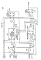
- FIG 7 shows a detailed logic diagram of a portion of the interrupt request register (IRR) 66 shown in Figure 2.
- the IRR 66 is made up of eight stages, each stage corresponding with one interrupt request input.
- One typical stage 212 is depicted in Figure 7.
- the IRR 66 in its entirety includes eight stages, such as those depicted in Figure 7.
- a programmable interrupt controller in accordance with the invention could include any suitable number of such stages.
- Figure 7 includes hardware designed to detect edge-triggered interrupt requests and also hardware to detect level-triggered interrupt requests.
- an input signal 214 called LEVEL/EDGE IRQ n .
- This signal indicates whether an interrupt request input corresponding to the stage 212 is edge-triggered or level-triggered.
- the LEVEL/EDGE IRQ n signal 214 could be any of the eight output signals of the ICW5 register 108 shown in Figure 6.
- an input signal IRQ n 216 is shown. This is an interrupt request input and could be any one of the interrupt request inputs 68 shown in Figure 2.
- an appropriate portion of the hardware depicted in Figure 7 is used for detecting the interrupt request and latching it into the appropriate bit of the IRR 66.
- the LEVEL/EDGE IRQ n signal 214 is high, thereby enabling the interrupt request IRQ n 216 through an AND gate 218 and an OR gate 220 to a metastability latch 222 at a data input 224.
- the metastability latch 222 is clocked by means of the system BCLK and the system CCLK as enabled by a FREEZE signal 226 through an AND gate 228.
- FREEZE 226 is normally high and goes low only during interrupt acknowledge cycles during which detection of a level-triggered interrupt request may be postponed.
- the output of the metastability latch 222 passes through an OR gate 230 to an input of an AND gate 232.
- the remaining inputs of the AND gate 232 include the ICW1 signal which is high except during the programming sequence for the ICW registers 94, and SETISRn 234. This latter signal is a pulse which is normally high but goes low when a corresponding bit of the in service register (ISR) 88 shown in Figure 2 is set.
- the output of the metastability latch 222 passes through the AND gate 232 to a data input of an interrupt request register (IRR) latch 236.
- This latch 236 stores the interrupt request so that the interrupt controller 8 can utilize it to interrupt the CPU 4 and provide suitable information for the CPU 4 to determine which interrupt service routine to execute.
- the IRR bit is reset and the ISR bit is set. If the automatic end of interrupt (AEOI) mode is selected by programming the AEOI bit 180 of the ICW4 register high, the ISR bit is cleared at the end of the final INTA pulse. Otherwise, the ISR bit is cleared when an appropriate EOI command is issued by the interrupt service routine.
- FREEZE goes high, the CCLK is passed to the C input of the metastability latch 222.
- the data input to the IRR latch 236 is enabled through the OR gate 229 and AND gate 232. Thus, the output of the metastability latch 222 is latched into the IRR latch 236.
- edge-triggered operation the hardware in the lower portion of Figure 7, described previously, works essentially as described. However, the hardware in the upper portion of the drawing detects and latches an edge-triggered interrupt request and provides the latched interrupt request to an input of the OR gate 220.
- An edge-triggered interrupt request is enabled by LEVEL/EDGE IRQ n signal 214 as inverted by an inverter 238 through an AND gate 240 to an input of an edge detector 242.
- the output of the edge detector 242 is connected through an OR gate 244 to an input of a level converter 246.
- Figures 8A and 8B show two preferred embodiments of the edge detector 242 of Figure 7.
- a latch 248 and an AND gate 250 having inputs connected to the input and the low-true output of the latch 248.
- the IRQ n signal 216 makes a transition from a low state to a high state. In order for a valid edge to be detected, the transition must take place within a specified time limit, such as one clock cycle.
- the system CCLK and BCLK continually run, latching the input signal into the latch 248.
- the output of the level converter 246 is then connected to an input of the OR gate 220. From here on, the latched edge-triggered interrupt is treated as if it were a level-triggered interrupt as described previously.
- FIG. 8B a second embodiment of the edge detector 242 is shown.
- This embodiment differs from that of Figure 8A in that a synchronizing latch 254 is connected ahead of the latch 248.
- the IRQ n input is connected to a data input of the synchronizing latch 254, and an output of the synchronizing latch 254 is connected to an input of the edge detector latch 248 and to the AND gate 250.
- the latch 248 and the AND gate 250 work essentially the same way as those of the embodiment of Figure 8A.
- the difference is that the synchronizing latch 254 synchronizes the edge-triggered interrupt request in terms of the systems CCLK and BCLK. This provides greater reliability of operation and permits the timing characteristics of the synchronizing latch 254 to be determined in accordance with the timing characteristics of the edge-triggered interrupt request IRQ n .
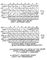
- Figures 9A-9E are tables showing typical initialization command word programming sequences for various system configurations.
- ICW1, ICW4, and ICW5 registers 100, 106, 108 the ICW2 and ICW3 registers 102, 104 are shown.
- the salient characteristics of the configuration are written out on the right, and bits which have certain required values for implementing those system configurations are identified along with the required values.
- the programmable interrupt controller 8 is configured for the cascade mode.
- bit 1 of ICW1, SINGLE/CASCADE bit 124 is set to zero.
- the controller 8 is also configured for operation along with Intel 8080 or 8085 microprocessors.
- the uPM bit 176, bit 0 of ICW4, is zero.
- the ICW2 register and the three most significant bits of the ICW1 register 100 are programmed with bits A15-A5 which provide the address of a page of memory having a table of interrupt service routine addresses.
- An address interval (ADI) bit, bit 2 of ICW1 may be is a one, indicating an interval of four bytes between interrupt service routine addresses, or a zero, indicating an interval of eight bytes between interrupt service routine addresses. In this latter case, bit 5 of the ICW1 register 100 is not used.
- the interrupt controller 8 is set to the cascade mode and a master and one or more slave interrupt controllers are employed, this particular interrupt controller 8 is programmed to be the master. This is done by setting the buffered mode bit BUF, bit 3 of ICW4, to a one and setting the M/S bit 178, bit 2 of ICW4, to a one.
- FIG. 9B there is shown a programming configuration identical to that of Figure 9A except that the programmable interrupt controller 8 is configured for use with 8086 and 8088 microprocessors. The difference is that bit 0 of ICW4, the uPM bit 176, is a one.
- bit 0 of ICW4 the uPM bit 176
- bits 3-7 of the ICW2 register 102 contain the five most significant bits of an interrupt vector supplied to the CPU 4. The three least significant bits, which make up the remainder of the interrupt vector, are determined by which interrupt request line IRQ n 216 is active.
- FIG. 9C there is shown a programming configuration identical to that of Figure 9A except that the interrupt controller 8 is configured to be a slave. This is done simply by setting the M/S bit 178, bit 2 of ICW4, to zero.
- FIG. 9D there is shown a configuration similar that of Figure 9A except that instead the cascade mode, the interrupt controller 8 is configured to the single mode. This is done by setting the SINGLE/CASCADE bit 124, bit 1 of ICW1, to a one. Similarly, the buffered mode bit, bit 3 of ICW4, is set to zero because the buffered mode is not applicable here. Also, the value of the M/S bit 178 is irrelevant. It should be noted that the ICW3 register 104 has been omitted from the programming sequence shown in Figure 9D. ICW3 contains information which is only pertinent when both a master and one or more slave interrupt controllers are present.
- the ICW3 register 104 contains eight bits S7-S0 which are set to indicate whether each of the corresponding interrupt request inputs has a slave controller attached to it.
- the ICW3 register 104 contains eight bits S7-S0 which are set to indicate whether each of the corresponding interrupt request inputs has a slave controller attached to it.
- only bits 2-0 of the ICW3 register 104 are used. These three bits provide a slave ID the value of which corresponds to the interrupt request input of the master interrupt controller to which the slave device is connected.
- the ICW3 register 104 is omitted in the single mode.
- FIG. 9E there is shown a programming configuration in which the ICW4 register 106 is omitted. Whether ICW4 is programmed is determined by the IC4 bit, bit 0 of ICW1. In Figures 9A-9D, this bit has always been set high. In Figure 9E, however, this bit is zero. Accordingly, the ICW4 register 106 is omitted and certain default values are established for bits appearing in the ICW4 register 106. First of all, the system is configured as though bit 0 of ICW4 were set to zero, indicating 8080/8085 microprocessor. Second, the system is configured as though the buffer bit, bit 3 of ICW4, were zero, i.e., the system is configured for a non-buffered mode.
- the hardware signal SP/EN is treated as an input and its state determines whether the interrupt controller is configured as a master of a slave. In the case of Figure 9E, it is assumed that the signal is high. Based on this assumption, the interrupt controller configures itself as a master.
- a programmable interrupt controller having a plurality of interrupt request inputs capable of detecting either edge-triggered or level-triggered interrupt requests from peripheral devices.
- the ICW5 register 108 has a bit corresponding with each interrupt request input.
- the bits may be programmed to one of two states respectively corresponding to edge-triggering or level-triggering.
- the bits are programmable on a per bit basis. Accordingly, the interrupt request inputs of the interrupt controller may be programmed on a per interrupt basis for either level-sensitivity or edge-sensitivity.
- the interrupt request inputs may be programmed for edge-sensitivity or level-sensitivity in this manner, it is possible to upgrade a system employing the interrupt controller by changing the mix of edge-triggered or level-triggered interrupt requests.
- the system remains backward compatible with older edge-triggered peripheral devices while accommodating newer level-triggered peripheral devices.
- the interrupt controller may be configured in a manner consistent with the Intel 8259A interrupt controller.
- the controller in accordance with the invention is backward compatible with software written for programming the 8259A.
- interrupt controllers may embody the invention by providing a plurality of interrupt request inputs programmable on a per interrupt basis for either edge-sensitivity or level-sensitivity in any manner suitable to the architecture of that particular interrupt controller.
Landscapes
- Engineering & Computer Science (AREA)
- Theoretical Computer Science (AREA)
- Physics & Mathematics (AREA)
- General Engineering & Computer Science (AREA)
- General Physics & Mathematics (AREA)
- Bus Control (AREA)
- Programmable Controllers (AREA)
Claims (10)
- Contrôleur d'interruption (8) destiné à un système d'ordinateur comportant une unité centrale de traitement (UC) (4), le contrôleur comprenant : une pluralité d'entrées (42, 56) reliées de façon à recevoir des demandes d'interruptions provenant d'une pluralité de dispositifs périphériques (26, 40), un moyen (66) destiné à envoyer un signal d'interruption vers l'unité centrale de traitement (4) sur une sortie de demandes d'interruptions (58) en réponse à l'une quelconque des demandes d'interruptions, un dispositif de définition de priorité (92) destiné à affecter à chaque entrée parmi la pluralité des entrées (42, 56) une position de priorité afin de créer une hiérarchie, dans le but de définir quelle demande d'interruption est desservie en premier lorsque des demandes d'interruptions se chevauchant dans le temps sont reçues, et un moyen (94) destiné à établir indépendamment chaque entrée de façon à ce qu'elle réponde à des demandes d'interruptions soit déclenchées par un front, soit déclenchées par un niveau, le moyen (94) destiné à établir comprenant un premier registre de commande d'initialisation (108) comportant une pluralité de bits, chaque bit correspondant respectivement à l'une des entrées (56, 42), et dans lequel chaque entrée est établie de façon à répondre à des demandes d'interruptions déclenchées par un front lorsque le bit respectif est dans un premier état et chaque entrée est établie de façon à répondre à des demandes d'interruptions déclenchées par un niveau lorsque le bit respectif est dans un second état,
le contrôleur d'interruption (8) étant caractérisé en ce que le moyen destiné à établir comprend un registre de demandes d'interruptions (66) comportant une pluralité d'étages, un étage respectif parmi les étages correspondant à chaque bit et à chaque entrée de demandes d'interruptions, chacun des étages comprenant :(a) un détecteur de front (242) comprenant un circuit à verrouillage de détecteur de front (248) comportant une entrée de données reliée à l'entrée de demandes d'interruptions respective et une sortie de donnée, et agissant lorsque le bit respectif du premier registre de commande d'initialisation (108) est programmé dans le premier état afin de recevoir une demande d'interruption sensible au front et mémorisant la demande vers un circuit à verrouillage de convertisseur en niveau (246) relié de façon à recevoir et à mémoriser une demande d'interruption sous forme d'un niveau.(b) un circuit à verrouillage à métastabilité (222) relié de façon à recevoir une demande d'interruption déclenchée par un niveau lorsque le bit respectif est programmé dans le second état et relié de façon à recevoir la demande d'interruption conservée sous forme d'un niveau par le circuit à verrouillage de convertisseur en niveau (246) lorsque le bit respectif est programmé dans le premier état, et(c) un circuit à verrouillage de registre de demandes d'interruptions (236) relié de façon à recevoir et à conserver la demande d'interruption qui a été conservée par le circuit à verrouillage à métastabilité (222). - Contrôleur d'interruption (8) selon la revendication 1, dans lequel le moyen destiné à établir comprend un second registre de commande d'initialisation (100) qui comprend un bit présentant un premier état correspondant aux interruptions sensibles au front et un second état correspondant à un type de sensibilité d'interruption qui peut être sélectionné par bit, dans lequel, lorsque le bit du second registre de commande d'initialisation (100) est dans le premier état, le détecteur de front (242) de chaque état est rendu fonctionnel et le circuit à verrouillage à métastabilité (222) est relié de façon à recevoir la demande d'interruption sensible au front du circuit à verrouillage, et dans lequel, lorsque le bit du second registre de commande d'initialisation (100) est dans le second état, le détecteur de front est rendu fonctionnel suivant l'état du bit respectif du premier registre de commande d'initialisation (108) et le circuit à verrouillage à métastabilité (222) est relié suivant l'état du bit respectif du premier registre de commande d'initialisation.
- Contrôleur d'interruption (8) selon la revendication 1, dans lequel le détecteur de front (242) comprend un circuit à verrouillage de synchronisation (254) ayant une entrée de données reliée de façon à recevoir la demande d'interruption respective lorsque le bit respectif du premier registre de commande d'initialisation (108) est programmé dans le premier état, une sortie de données reliée à une entrée de données du circuit à verrouillage de détecteur de front (248), et une entrée d'horloge reliée de façon à recevoir une horloge du système afin de mémoriser une demande d'interruption allant de l'entrée de données vers la sortie de données, d'où il résulte que le circuit à verrouillage de synchronisation (254) mémorise un signal de demande d'interruption déclenchée par un front vers l'entrée de données du circuit à verrouillage de détecteur de front (248) en synchronisme avec l'horloge du système.
- Contrôleur d'interruption (8) selon la revendication 2 comprenant une mémoire tampon de bus de données (62) reliée à un bus de données du système (2), le bus de données du système étant relié à l'unité centrale de traitement (UC) (4), un bus de données interne (64) relié entre la mémoire tampon de bus de données (62) et un module logique de commandes de lecture/écriture (74), le module (74) comprenant en outre un moyen destiné à écrire des données qui sont sur le bus de données du système (2) jusque dans les premier et second registres de commande d'initialisation (94) par l'intermédiaire de la mémoire tampon de bus de données (62) et du bus de données interne (64), en réponse aux commandes provenant de l'unité centrale de traitement (4).
- Contrôleur d'interruption (8) selon la revendication 4, dans lequel le module logique de commande de lecture/écriture (74) comprend une seconde sortie d'interruptions présentant des premier et second états de sortie, la seconde sortie d'interruptions entrant dans le premier état lorsqu'un bit de registre de demandes d'interruptions reçoit et conserve une demande d'interruption, en interrompant ainsi l'unité centrale de traitement (4) de façon à amener l'unité centrale de traitement (4) à desservir la demande d'interruption.
- Contrôleur d'interruption selon la revendication 1, dans lequel les bits sont programmables bit par bit entre les premier et second états.
- Système d'ordinateur comprenant :une unité centrale de traitement (UC) (4) comportant un moyen de commande comprenant une pluralité de sous-programmes de services d'interruptions destinés à desservir des demandes d'interruptions,une pluralité de dispositifs périphériques (26, 40) comprenant des premiers dispositifs périphériques destinés à générer des demandes d'interruptions déclenchées par un front et des seconds dispositifs périphériques destinés à générer des demandes d'interruptions déclenchées par un niveau,un bus (2) relié à l'unité centrale de traitement (4),un contrôleur d'interruption (8) selon l'une quelconque des revendications précédentes, relié aux dispositifs périphériques (26, 40) et au bus, afin d'interrompre l'unité centrale de traitement en réponse aux demandes d'interruptions déclenchées par un front provenant des périphériques et destiné à amener l'unité centrale de traitement à exécuter les sous-programmes de services d'interruptions.
- Procédé destiné à recevoir et à desservir une demande d'interruption déclenchée par un front provenant d'une première source et une demande d'interruption déclenchée par un niveau provenant d'une seconde source, comprenant les étapes consistant à :programmer un contrôleur d'interruption comportant des première et seconde entrées de demandes d'interruptions afin de détecter des demandes d'interruptions déclenchées par un front arrivant sur la première entrée de demandes d'interruptions et de détecter des demandes d'interruptions déclenchées par un niveau arrivant sur la seconde entrée de demandes d'interruptions, la programmation étant exécutée sur un principe dépendant de l'entrée,détecter et mémoriser une demande d'interruption déclenchée par un front arrivant sur la première entrée,interrompre une unité centrale de traitement (UC) pour amener l'unité centrale de traitement à desservir la demande d'interruption déclenchée par un front,détecter une demande d'interruption déclenchée par un niveau arrivant sur la seconde entrée,interrompre l'unité centrale de traitement pour amener l'unité centrale de traitement à desservir la demande d'interruption déclenchée par un niveau,charger la demande d'interruption déclenchée par un front mémorisée dans un premier bit d'un registre de demandes d'interruptions correspondant à la première entrée de demandes d'interruptions, etcharger la demande d'interruption déclenchée par un niveau dans un second bit d'un registre de demandes d'interruptions correspondant à la seconde entrée de demandes d'interruptions.
- Procédé selon la revendication 8, dans lequel l'étape consistant à programmer comprend l'établissement des premier et second bits d'un registre de commande d'initialisation, correspondant respectivement aux première et seconde entrées dans des premier et second états, respectivement, le premier état correspondant à un déclenchement par un front, et le second état correspondant à un déclenchement par un niveau.
- Procédé selon la revendication 9, dans lequel les première et seconde entrées de demandes d'interruptions comportent des premier et second octets de vecteurs d'interruptions correspondant respectivement à celles-ci, et les étapes consistant à exécuter l'interruption pour desservir les demandes d'interruptions déclenchées par un front et déclenchées par un niveau comprennent chacune la validation de l'octet de vecteur d'interruption respectif sur le bus de données.
Applications Claiming Priority (2)
| Application Number | Priority Date | Filing Date | Title |
|---|---|---|---|
| US43127589A | 1989-11-03 | 1989-11-03 | |
| US431275 | 1989-11-03 |
Publications (3)
| Publication Number | Publication Date |
|---|---|
| EP0426331A2 EP0426331A2 (fr) | 1991-05-08 |
| EP0426331A3 EP0426331A3 (en) | 1991-11-06 |
| EP0426331B1 true EP0426331B1 (fr) | 1997-10-01 |
Family
ID=23711223
Family Applications (1)
| Application Number | Title | Priority Date | Filing Date |
|---|---|---|---|
| EP90311376A Expired - Lifetime EP0426331B1 (fr) | 1989-11-03 | 1990-10-17 | Dispositif et procédé de commande d'interruption programmable |
Country Status (9)
| Country | Link |
|---|---|
| EP (1) | EP0426331B1 (fr) |
| JP (1) | JPH0612526B2 (fr) |
| KR (1) | KR940002087B1 (fr) |
| CN (1) | CN1020813C (fr) |
| AU (1) | AU635338B2 (fr) |
| BR (1) | BR9005533A (fr) |
| DE (1) | DE69031530D1 (fr) |
| GB (1) | GB9012950D0 (fr) |
| MY (1) | MY107293A (fr) |
Families Citing this family (13)
| Publication number | Priority date | Publication date | Assignee | Title |
|---|---|---|---|---|
| AU706450B2 (en) * | 1993-07-06 | 1999-06-17 | Tandem Computers Incorporated | A processor interface circuit |
| JP2921412B2 (ja) * | 1994-09-30 | 1999-07-19 | 日本電気株式会社 | データ処理装置 |
| KR100393765B1 (ko) * | 1996-03-26 | 2004-03-10 | 엘지전자 주식회사 | 인터럽트제어장치 |
| US6298410B1 (en) * | 1997-12-31 | 2001-10-02 | Intel Corporation | Apparatus and method for initiating hardware priority management by software controlled register access |
| CN100437394C (zh) * | 2006-04-14 | 2008-11-26 | 华为技术有限公司 | 一种硬件单元的控制方法 |
| CN101872330B (zh) * | 2009-11-04 | 2012-07-25 | 杭州海康威视数字技术股份有限公司 | 多pcie设备系统中断处理方法 |
| CN102200770B (zh) * | 2011-04-06 | 2013-04-10 | 北京配天大富精密机械有限公司 | 一种基于pci的信息交互系统及方法、上位机 |
| US20120271968A1 (en) * | 2011-04-21 | 2012-10-25 | Microchip Technology Incorporated | Logic device for combining various interrupt sources into a single interrupt source and various signal sources to control drive strength |
| US9450585B2 (en) | 2011-04-20 | 2016-09-20 | Microchip Technology Incorporated | Selecting four signals from sixteen inputs |
| CN102693193B (zh) * | 2012-04-26 | 2015-05-27 | 重庆重邮信科通信技术有限公司 | 中断辅助处理装置、实时系统及中断处理方法 |
| CN103617137B (zh) * | 2013-11-29 | 2016-09-07 | 暨南大学 | 一种兼容8051 ip核的中断控制器及其控制方法 |
| CN105278408B (zh) * | 2015-10-26 | 2017-07-25 | 重庆电子工程职业学院 | 一种基于计算机ic控制的多功能定时器电路 |
| CN107463494B (zh) * | 2017-06-30 | 2020-11-03 | 百富计算机技术(深圳)有限公司 | 中断服务程序调试方法、装置、存储介质及其计算机设备 |
Family Cites Families (3)
| Publication number | Priority date | Publication date | Assignee | Title |
|---|---|---|---|---|
| JPS5741726A (en) * | 1980-08-22 | 1982-03-09 | Hitachi Ltd | Process interruption input circuit |
| PH24865A (en) * | 1987-03-24 | 1990-12-26 | Ibm | Mode conversion of computer commands |
| CA1319441C (fr) * | 1988-09-09 | 1993-06-22 | Paul R. Culley | Controleur d'interruption programmable |
-
1990
- 1990-06-11 GB GB909012950A patent/GB9012950D0/en active Pending
- 1990-10-03 AU AU63757/90A patent/AU635338B2/en not_active Ceased
- 1990-10-03 MY MYPI90001722A patent/MY107293A/en unknown
- 1990-10-11 JP JP2273107A patent/JPH0612526B2/ja not_active Expired - Lifetime
- 1990-10-17 EP EP90311376A patent/EP0426331B1/fr not_active Expired - Lifetime
- 1990-10-17 DE DE69031530T patent/DE69031530D1/de not_active Expired - Lifetime
- 1990-10-31 BR BR909005533A patent/BR9005533A/pt not_active Application Discontinuation
- 1990-10-31 KR KR1019900017520A patent/KR940002087B1/ko not_active Expired - Fee Related
- 1990-10-31 CN CN90108766A patent/CN1020813C/zh not_active Expired - Fee Related
Also Published As
| Publication number | Publication date |
|---|---|
| EP0426331A3 (en) | 1991-11-06 |
| DE69031530D1 (de) | 1997-11-06 |
| AU635338B2 (en) | 1993-03-18 |
| KR910010326A (ko) | 1991-06-29 |
| AU6375790A (en) | 1991-05-09 |
| CN1020813C (zh) | 1993-05-19 |
| BR9005533A (pt) | 1991-09-17 |
| EP0426331A2 (fr) | 1991-05-08 |
| JPH03196225A (ja) | 1991-08-27 |
| KR940002087B1 (ko) | 1994-03-17 |
| GB9012950D0 (en) | 1990-08-01 |
| JPH0612526B2 (ja) | 1994-02-16 |
| MY107293A (en) | 1995-10-31 |
| CN1052202A (zh) | 1991-06-12 |
Similar Documents
| Publication | Publication Date | Title |
|---|---|---|
| US5261107A (en) | Programable interrupt controller | |
| EP0157075B1 (fr) | Système modulaire de traitement de données | |
| EP0006472B1 (fr) | Dispositif de microcommande pour commander le transfer bidirectionnel entre une unité de contrôle centrale et une pluralité d'unités externes | |
| US6219742B1 (en) | Method and apparatus for artificially generating general purpose events in an ACPI environment | |
| US4716527A (en) | Bus converter | |
| EP0192944B1 (fr) | Système de traitement de données avec un processeur principal et un co-processeur utilisant en commun les mêmes ressources | |
| EP0426331B1 (fr) | Dispositif et procédé de commande d'interruption programmable | |
| US6457069B1 (en) | Method and apparatus for providing support for dynamic resource assignment and configuration of peripheral devices when enabling or disabling plug-and-play aware operating systems | |
| JP2610812B2 (ja) | データ処理システムのエミユレーシヨン | |
| KR100385871B1 (ko) | 인터럽트 제어기 | |
| US5628027A (en) | Method of determining the configuration of devices installed on a computer bus | |
| US6070204A (en) | Method and apparatus for using universal serial bus keyboard to control DOS operations | |
| US4888680A (en) | Peripheral device interface and controller | |
| US5675772A (en) | Device and method for reconfiguring a computer system with an incompatible CPU | |
| US20010018721A1 (en) | Upgrade card for a computer system | |
| WO1996000940A1 (fr) | Convertisseur de protocole d'interruptions pci en protocole d'interruptions isa et logique de selection | |
| JPS6258028B2 (fr) | ||
| EP0437550B1 (fr) | Methode et appareil d'emulation pour un systeme de traitement de l'information | |
| KR950001417B1 (ko) | 컴퓨터 시스템 | |
| JPS6319854Y2 (fr) | ||
| US6457137B1 (en) | Method for configuring clock ratios in a microprocessor | |
| EP0676687B1 (fr) | Unités de gestion d'alimentation pour systèmes d'ordinateur | |
| JPH07104830B2 (ja) | コンピュータ・システム及びコンピュータ・システムを作動させる方法 | |
| CN113311931B (zh) | 一种方便iap的双复位向量8位mcu架构及其方法 | |
| Mustafa | Microcomputer interfacing and applications |
Legal Events
| Date | Code | Title | Description |
|---|---|---|---|
| PUAI | Public reference made under article 153(3) epc to a published international application that has entered the european phase |
Free format text: ORIGINAL CODE: 0009012 |
|
| 17P | Request for examination filed |
Effective date: 19901213 |
|
| AK | Designated contracting states |
Kind code of ref document: A2 Designated state(s): DE FR GB IT |
|
| PUAL | Search report despatched |
Free format text: ORIGINAL CODE: 0009013 |
|
| AK | Designated contracting states |
Kind code of ref document: A3 Designated state(s): DE FR GB IT |
|
| RHK1 | Main classification (correction) |
Ipc: G06F 13/24 |
|
| 17Q | First examination report despatched |
Effective date: 19940711 |
|
| GRAG | Despatch of communication of intention to grant |
Free format text: ORIGINAL CODE: EPIDOS AGRA |
|
| GRAH | Despatch of communication of intention to grant a patent |
Free format text: ORIGINAL CODE: EPIDOS IGRA |
|
| GRAH | Despatch of communication of intention to grant a patent |
Free format text: ORIGINAL CODE: EPIDOS IGRA |
|
| GRAA | (expected) grant |
Free format text: ORIGINAL CODE: 0009210 |
|
| AK | Designated contracting states |
Kind code of ref document: B1 Designated state(s): DE FR GB IT |
|
| PG25 | Lapsed in a contracting state [announced via postgrant information from national office to epo] |
Ref country code: IT Free format text: LAPSE BECAUSE OF FAILURE TO SUBMIT A TRANSLATION OF THE DESCRIPTION OR TO PAY THE FEE WITHIN THE PRE;WARNING: LAPSES OF ITALIAN PATENTS WITH EFFECTIVE DATE BEFORE 2007 MAY HAVE OCCURRED AT ANY TIME BEFORE 2007. THE CORRECT EFFECTIVE DATE MAY BE DIFFERENT FROM THE ONE RECORDED.SCRIBED TIME-LIMIT Effective date: 19971001 Ref country code: FR Free format text: LAPSE BECAUSE OF FAILURE TO SUBMIT A TRANSLATION OF THE DESCRIPTION OR TO PAY THE FEE WITHIN THE PRESCRIBED TIME-LIMIT Effective date: 19971001 |
|
| REF | Corresponds to: |
Ref document number: 69031530 Country of ref document: DE Date of ref document: 19971106 |
|
| PG25 | Lapsed in a contracting state [announced via postgrant information from national office to epo] |
Ref country code: DE Free format text: LAPSE BECAUSE OF FAILURE TO SUBMIT A TRANSLATION OF THE DESCRIPTION OR TO PAY THE FEE WITHIN THE PRESCRIBED TIME-LIMIT Effective date: 19980103 |
|
| EN | Fr: translation not filed | ||
| PLBE | No opposition filed within time limit |
Free format text: ORIGINAL CODE: 0009261 |
|
| STAA | Information on the status of an ep patent application or granted ep patent |
Free format text: STATUS: NO OPPOSITION FILED WITHIN TIME LIMIT |
|
| 26N | No opposition filed | ||
| PGFP | Annual fee paid to national office [announced via postgrant information from national office to epo] |
Ref country code: GB Payment date: 19990930 Year of fee payment: 10 |
|
| PG25 | Lapsed in a contracting state [announced via postgrant information from national office to epo] |
Ref country code: GB Free format text: LAPSE BECAUSE OF NON-PAYMENT OF DUE FEES Effective date: 20001017 |
|
| GBPC | Gb: european patent ceased through non-payment of renewal fee |
Effective date: 20001017 |