EP0425303A2 - Delay measuring circuit - Google Patents
Delay measuring circuit Download PDFInfo
- Publication number
- EP0425303A2 EP0425303A2 EP90311759A EP90311759A EP0425303A2 EP 0425303 A2 EP0425303 A2 EP 0425303A2 EP 90311759 A EP90311759 A EP 90311759A EP 90311759 A EP90311759 A EP 90311759A EP 0425303 A2 EP0425303 A2 EP 0425303A2
- Authority
- EP
- European Patent Office
- Prior art keywords
- delay
- output
- input
- signal
- value
- Prior art date
- Legal status (The legal status is an assumption and is not a legal conclusion. Google has not performed a legal analysis and makes no representation as to the accuracy of the status listed.)
- Granted
Links
Images
Classifications
-
- G—PHYSICS
- G01—MEASURING; TESTING
- G01R—MEASURING ELECTRIC VARIABLES; MEASURING MAGNETIC VARIABLES
- G01R25/00—Arrangements for measuring phase angle between a voltage and a current or between voltages or currents
- G01R25/08—Arrangements for measuring phase angle between a voltage and a current or between voltages or currents by counting of standard pulses
-
- G—PHYSICS
- G01—MEASURING; TESTING
- G01R—MEASURING ELECTRIC VARIABLES; MEASURING MAGNETIC VARIABLES
- G01R29/00—Arrangements for measuring or indicating electric quantities not covered by groups G01R19/00 - G01R27/00
- G01R29/02—Measuring characteristics of individual pulses, e.g. deviation from pulse flatness, rise time or duration
- G01R29/027—Indicating that a pulse characteristic is either above or below a predetermined value or within or beyond a predetermined range of values
- G01R29/0273—Indicating that a pulse characteristic is either above or below a predetermined value or within or beyond a predetermined range of values the pulse characteristic being duration, i.e. width (indicating that frequency of pulses is above or below a certain limit)
Definitions
- This invention relates to delay measuring circuits.
- the invention has a particular application to integrated circuits wherein a large number of individual cells are implemented on a single chip, the chip circuitry including such cells in the circuit implemented on the chip.
- Production process variation and temperature and power voltage supply fluctuations are the same for every cell on one chip.
- all these cells have the same characteristics, such as switching levels and propagation delay, the relative delay between individual cells being minimal.
- production process variations and temperature and power supply voltage fluctuations can cause a large absolute delay difference between two integrated circuit chips.
- circuit designs needing accurate absolute delays cannot generally be implemented on integrated circuit chips.
- European Patent Application No. 0 173 521 discloses a clock signal distribution system employing a plurality of clock distribution chips responsive to a main clock signal.
- the system provides for the clock signals generated by each chip to be automatically adjusted to be delayed by an amount corresponding to the delay provided by an accurate filed delay external to the chip, such as a fixed length of wire.
- an accurate filed delay external to the chip such as a fixed length of wire.
- the clock signals provided by all the clock distribution chips are synchronized with one other.
- each chip includes a multitapped delay line, a phase comparator, a multiplexer having inputs connected to the delay line taps and a counter.
- the phase comparator compares the phase of the output of the external fixed delay with toe clock signal generated by the chip, the arrangement being such that the counter controls the multiplexer to select an appropriate tap signal output to provide a clock signal delay corresponding to the fixed, external delay.
- a delay measuring circuit characterized by input means adapted to receive an applied clock signal, and coupled to a delay line having a plurality of individual delay cells, with outputs thereof respectively connected to inputs of a switching device, said input means being further connected to an input of counter means and to a delay device having a delay substantially equal to the intrinsic delay of said switching device, wherein said counter means has output means coupled to latch means and to a plurality of control inputs of said switching device to thereby connect a selected input of said switching device to an output thereof, and in that phase comparator means are provided having inputs coupled to said output of said switching device and to an output of said delay device, an output of said phase comparator means being coupled to said counter means and to said latch means, whereby in response to a phase comparison match, the count value in said counter means is latched into said latch means and said counter means is reset to a predetermined value, such that said latch means stores a value dependent on the delay of one of said individual delay cells.
- a delay measuring circuit finds application in a plurality of environments. Two exemplary applications, will be described hereinafter A first application is in a timing watchdog circuit, wherein an alarm signal is generated when the timing of an integrated circuit falls below a predetermined safety level. A second application permits the generation of signals having a delay equal to a predetermined fraction of a reference clock signal.
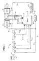
- the circuit 10 includes an input line 12 to which is applied in operation a reference clock signal 13 having a fixed period T.
- the input line 12 is connected to the input of a delay line 14 which includes a plurality N of identical, series-connected delay cells 16, identified respectively as 16-1 to 16-N, each having a delay time of D.
- the construction of such delay cells is well known.
- each delay cell could be implemented as a buffer cell or alternatively as an AND gate, and formed by field effect transistors in an integrated circuit, such as a CMOS circuit.
- the input line 12 is connected via lines 18, 20 to a counter 22.
- the outputs of the delay cells 16-1 to 16-N are connected via respective lines 24-1 to 24-N to N inputs of a switch 26 having a single output connected to an output line 28.
- the counter 22 is an A-bit binary counter having A outputs, connected via A lines 30 to respective control inputs of the switch 26. It should be understood that the operation of the switch 26 is such that a selected one o£ the N inputs thereof is connected to the output line 28, in dependence on the signals applied over the lines 30 to the A control inputs of the switch 26.
- the output lines of the counter 22 are also connected to the inputs of a latch Circuit 32 having A output lines 33.
- the output line 28 of the switch 26 is connected to a first input of a phase comparator circuit 34 having a second input which is coupled over a line 36 to the output of a delay circuit 38, the input of which is coupled to the line 18 and hence receives the applied clock signal 13.
- the delay circuit 38 is constructed to provide a delay d which is equal to the intrinsic delay d of the switch 26, that is, the delay d which results to signals passing from any one of the N inputs of the switch 26 to the output thereof.
- the output of the phase comparator 34 is connected via a line 40 to a reset input 42 of the counter 22, whereby the counter is reset to a predetermined count value of 5.
- the value S may be hardwired or loaded into the counter stages by logic incorporated in the counter 22.
- the output of the phase comparator 34 is also connected via the line 40 to a control input 44 of the latch 32 whereby the value present on the lines 30 may be stored in the latch 32.
- the circuit 10 measures the number of delay cells 16 which provide a cumulative delay equal to one period T of the reference clock signal 13. This operation will now be explained. It is assumed that the counter 22 is initially at the predetermined value S. With this value S in the counter 22, the switch 26 is effective to connect its input number S to the output line 28, that is, the output of delay cell number S is connected to the switch output line 28. Consequently, the output line 28 of the switch 26 will carry a signal which corresponds to the reference clock 13 delayed by the delay of S delay cells, that is, a delay of D.S, plus the intrinsic delay d of the switch 26.
- the count value on the counter 22 is incremented to the value S+1 on the next positive-going reference clock transistion, and a further phase comparison is effected in the phase comparator 34. These steps are repeated until the phases of the input signals on the input lines 28, 36 to the phase comparator 34 match.
- the delay circuit 38 having a delay equal to the delay d, the intrinsic delay d of the switch 26 is compensated. It will be seen that, with the switch in position 5, the output signal on the line 28 is the reference clock signal 13 delayed by D.S + d. Since the phase comparator 34 compares the phase of the output signal of the switch 26 on the line 28 with the output signal of the delay circuit 38 on the line 36, it will be appreciated that the delay circuit 38 compensates for the delay inherent in the switch 26.
- the counter 22 is reset to the value S again and the incrementing of the counter 22 and phase comparison in the phase comparator 34 take place as described above.
- the period of the reference clock signal is arranged to be of a sufficiently small value such that the described counting and phase comparison are effected at such a speed that the repeated storing of the value X in the latch circuit 32 takes place at a speed which exceeds any temperature and power voltage fluctuations in the integrated circuit chip by an order of magnitude.
- the delay measuring circuit 10 when implemented on an integrated circuit chip thus continuously measures the number of delay cells 16 having a cumulative delay equal to one period T of the reference clock signal 13. Since production process variations and temperature and power supply voltage variations are substantially toe same for all cells on such a chip, all cells on the chip will have substantially the same characteristics (such as switching levels and propagation delay), with minimal variation between individual cells. However, production process variations and temperature and power supply voltage variations can cause a large absolute delay difference between two individual chips.
- the described delay measuring circuit provides a measure dependent on the absolute value of the delay of a delay cell.
- the delay measuring circuit 10 can be utilized in various applications, two of which will now be described in detail with reference to Fig. 2 and Fig. 3, respectively.
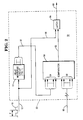
- a second embodiment of the invention implementing an application of the delay measuring circuit 10 to provide a timing watchdog or monitoring circuit 50 in an integrated circuit chip, such as a VLSI chip 52 containing various circuitry (not shown).
- the timing watchdog circuit of Fig. 2 provides an error flag alarm signal which enables corrective action to be taken should the timing of the VLSI chip become too slow.
- the timing watchdog circuit 50 includes the delay measuring circuit 10, described hereinabove with reference to Fig. 1.
- the output lines 33 of the latch circuit 32 (Fig. 1) are connected to a first set of inputs 54 of a comparator circuit 56, which has a second set of inputs 58 to which are applied signals from an A-bit bus 60, representing a maximum value M.
- the comparator 56 provides an output signal on a line 62 which is clocked into a latch circuit 64 by the next positive-going clock signal transition on the line 12, applied via a connecting line 66 to the clock input of the latch circuit 64.
- the latch circuit 64 now provides an error flag alarm signal over an output line 68.
- the timing watchdog circuit 50 may be used in high reliability environments where it is essential that the circuitry (not shown) in the VLSI chip 52 always meets a worst case timing requirement. Degradation of the chip 52 itself or excessive variation in temperature or supply voltage could result in the chip 52 no longer meeting the required worst case timing.
- the value M applied over the bus 60 is selected such that an error flag alarm signal is provided on the line 68 before substantial timing problems occur.
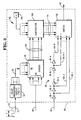
- FIG. 3 there is shown a third embodiment of the invention, implementing an application of the delay measuring circuit 10 to provide a programmable delay such that a reference clock signal 13 can be delayed by a predetermined fraction of the reference clock period.
- An integrated circuit chip 80 is shown in Fig. 3 as including a circuit 82 which generates a delay equal to a desired fraction of the reference clock period, such fraction being maintained despite temperature and power supply voltage fluctuations.
- an input signal on a line 84 is delayed by a predetermined fraction F of the period T of the reference clock signal 13.
- the integrated circuit chip 80 includes the delay measuring circuit 10, described hereinabove with reference to Fig. 1.
- the output lines 33 of the latch Circuit 32 (Fig. 1) are connected to a first set of inputs 88 of a divider circuit 90 having a second set of inputs 92, to which are applied the value F over a bus 94.
- the rne input signal line 84 is connected to the input of a delay line 96 which is identical in layout and construction to the delay line 14 included in the delay measuring circuit 10 (see Fig. 1).
- the delay line 96 includes N individual series-connected delay cells 98, identified as 98-1 to 98-N, respectively.
- the outputs of the delay cells 98-1 to 98-N are connected via respective lines 100-1 to 100-N to corresponding number inputs 1, 2, --, N of a switch 102.
- the output lines 104 of the divider circuit 90 are connected to a first set of inputs of a subtractor circuit 106, which has a second set of inputs coupled to receive a correction value C (to be explained) from a register 108, which may be a storage location provided in a memory device (not shown) included in the chip 80.
- the divider circuit 90 is effective to divide the number X, respresenting the number of delay cells 16 (Fig. 1) having a delay equal to the reference clock period T, by the number F, resulting in the number x/F (with the fractional part discarded), which number is used to control the number of effective delay cells 98 in the delay line 96, by appropriately controlling the switch 102, such that a number X/F of delay cells 98 are effectively connected between the input line 84 and the output line 86.
- the minimum selectable delay is determined by e/D. Since X/F must be larger than e/D.
- the delay cells 98 should be constructed to provide a delay D which is as small as possible.
Landscapes
- Physics & Mathematics (AREA)
- General Physics & Mathematics (AREA)
- Pulse Circuits (AREA)
Abstract
Description
- This invention relates to delay measuring circuits.
- The invention has a particular application to integrated circuits wherein a large number of individual cells are implemented on a single chip, the chip circuitry including such cells in the circuit implemented on the chip. Production process variation and temperature and power voltage supply fluctuations are the same for every cell on one chip. Thus, all these cells have the same characteristics, such as switching levels and propagation delay, the relative delay between individual cells being minimal. However, production process variations and temperature and power supply voltage fluctuations can cause a large absolute delay difference between two integrated circuit chips. Thus, circuit designs needing accurate absolute delays cannot generally be implemented on integrated circuit chips.
- European Patent Application No. 0 173 521 discloses a clock signal distribution system employing a plurality of clock distribution chips responsive to a main clock signal. The system provides for the clock signals generated by each chip to be automatically adjusted to be delayed by an amount corresponding to the delay provided by an accurate filed delay external to the chip, such as a fixed length of wire. Thus the clock signals provided by all the clock distribution chips are synchronized with one other. For this purpose, each chip includes a multitapped delay line, a phase comparator, a multiplexer having inputs connected to the delay line taps and a counter. The phase comparator compares the phase of the output of the external fixed delay with toe clock signal generated by the chip, the arrangement being such that the counter controls the multiplexer to select an appropriate tap signal output to provide a clock signal delay corresponding to the fixed, external delay.
- It is the object of the present invention to provide a delay measuring circuit which can be employed to improve the utilization of integrated circuit chips.
- Therefore according to the present invention, there is provided a delay measuring circuit, characterized by input means adapted to receive an applied clock signal, and coupled to a delay line having a plurality of individual delay cells, with outputs thereof respectively connected to inputs of a switching device, said input means being further connected to an input of counter means and to a delay device having a delay substantially equal to the intrinsic delay of said switching device, wherein said counter means has output means coupled to latch means and to a plurality of control inputs of said switching device to thereby connect a selected input of said switching device to an output thereof, and in that phase comparator means are provided having inputs coupled to said output of said switching device and to an output of said delay device, an output of said phase comparator means being coupled to said counter means and to said latch means, whereby in response to a phase comparison match, the count value in said counter means is latched into said latch means and said counter means is reset to a predetermined value, such that said latch means stores a value dependent on the delay of one of said individual delay cells.
- A delay measuring circuit according to the invention finds application in a plurality of environments. Two exemplary applications, will be described hereinafter A first application is in a timing watchdog circuit, wherein an alarm signal is generated when the timing of an integrated circuit falls below a predetermined safety level. A second application permits the generation of signals having a delay equal to a predetermined fraction of a reference clock signal.
- Embodiments of the invention will now be described by way of example, with reference to the accompanying drawings, in which:-
- Fig. 1 is block diagram of a delay measuring circuit according to the invention;
- Fig. 2 is a block diagram of a timing watchdog circuit utilizing the delay measuring circuit shown in Fig. 1; and
- Fig. 3 is a block diagram of a delay generating circuit utilizing the delay measuring circuit shown in Fig. 1.
- Referring first to Fig. 1, there is shown an embodiment of a
delay measuring circuit 10 according to the invention. Thecircuit 10 includes aninput line 12 to which is applied in operation areference clock signal 13 having a fixed period T. Theinput line 12 is connected to the input of adelay line 14 which includes a plurality N of identical, series-connecteddelay cells 16, identified respectively as 16-1 to 16-N, each having a delay time of D. The construction of such delay cells is well known. For example, each delay cell could be implemented as a buffer cell or alternatively as an AND gate, and formed by field effect transistors in an integrated circuit, such as a CMOS circuit. - The
input line 12 is connected vialines counter 22. The outputs of the delay cells 16-1 to 16-N are connected via respective lines 24-1 to 24-N to N inputs of aswitch 26 having a single output connected to anoutput line 28. - The
counter 22 is an A-bit binary counter having A outputs, connected viaA lines 30 to respective control inputs of theswitch 26. It should be understood that the operation of theswitch 26 is such that a selected one o£ the N inputs thereof is connected to theoutput line 28, in dependence on the signals applied over thelines 30 to the A control inputs of theswitch 26. - The output lines of the
counter 22 are also connected to the inputs of alatch Circuit 32 havingA output lines 33. Theoutput line 28 of theswitch 26 is connected to a first input of aphase comparator circuit 34 having a second input which is coupled over aline 36 to the output of adelay circuit 38, the input of which is coupled to theline 18 and hence receives theapplied clock signal 13. Thedelay circuit 38 is constructed to provide a delay d which is equal to the intrinsic delay d of theswitch 26, that is, the delay d which results to signals passing from any one of the N inputs of theswitch 26 to the output thereof. The output of thephase comparator 34 is connected via aline 40 to areset input 42 of thecounter 22, whereby the counter is reset to a predetermined count value of 5. The value S may be hardwired or loaded into the counter stages by logic incorporated in thecounter 22. The output of thephase comparator 34 is also connected via theline 40 to acontrol input 44 of thelatch 32 whereby the value present on thelines 30 may be stored in thelatch 32. - The
circuit 10 measures the number ofdelay cells 16 which provide a cumulative delay equal to one period T of thereference clock signal 13. This operation will now be explained. It is assumed that thecounter 22 is initially at the predetermined value S. With this value S in thecounter 22, theswitch 26 is effective to connect its input number S to theoutput line 28, that is, the output of delay cell number S is connected to theswitch output line 28. Consequently, theoutput line 28 of theswitch 26 will carry a signal which corresponds to thereference clock 13 delayed by the delay of S delay cells, that is, a delay of D.S, plus the intrinsic delay d of theswitch 26. - If the two inputs to the
phase comparator 34 do not match in phase, the count value on thecounter 22 is incremented to the value S+1 on the next positive-going reference clock transistion, and a further phase comparison is effected in thephase comparator 34. These steps are repeated until the phases of the input signals on theinput lines phase comparator 34 match. The count in thecounter 22 has the value X at this time. This implies that thereference clock 13, delayed with X times the delay of one delay cell, that is, delayed by a time X.D, and the (undelayed)reference clock 13, have the same phase. In this situation, the delay value X.D equals the reference clock period T, that is:
T = X.D.
This value X is stored in thelatch 32 in response to a match output signal on theoutput line 40 of thephase comparator 34, applied over thelatch control input 44. - It will now be appreciated that by providing the
delay circuit 38 having a delay equal to the delay d, the intrinsic delay d of theswitch 26 is compensated. It will be seen that, with the switch in position 5, the output signal on theline 28 is thereference clock signal 13 delayed by D.S + d. Since thephase comparator 34 compares the phase of the output signal of theswitch 26 on theline 28 with the output signal of thedelay circuit 38 on theline 36, it will be appreciated that thedelay circuit 38 compensates for the delay inherent in theswitch 26. - After the value X has been stored in the
latch circuit 32 thecounter 22 is reset to the value S again and the incrementing of thecounter 22 and phase comparison in thephase comparator 34 take place as described above. - In an application where the
delay measuring circuit 10 is implemented in an integrated circuit chip, such as a VLSI (very large scale integrated) chip, the period of the reference clock signal is arranged to be of a sufficiently small value such that the described counting and phase comparison are effected at such a speed that the repeated storing of the value X in thelatch circuit 32 takes place at a speed which exceeds any temperature and power voltage fluctuations in the integrated circuit chip by an order of magnitude. Thus, the value of X stored in thelatch Circuit 32 is always related to the delay D of adelay cell 16 by the expression X = T/D. Since the value of T is known and fixed, the actual delay of asignal delay cell 16 can be readily calculated with the aid of a divider unit or by a processor, if desired, using the value stored in thelatch circuit 32 and available on thelatch output lines 33, from the formula D = T/X. - The
delay measuring circuit 10, when implemented on an integrated circuit chip thus continuously measures the the number ofdelay cells 16 having a cumulative delay equal to one period T of thereference clock signal 13. Since production process variations and temperature and power supply voltage variations are substantially toe same for all cells on such a chip, all cells on the chip will have substantially the same characteristics (such as switching levels and propagation delay), with minimal variation between individual cells. However, production process variations and temperature and power supply voltage variations can cause a large absolute delay difference between two individual chips. The described delay measuring circuit provides a measure dependent on the absolute value of the delay of a delay cell. Thedelay measuring circuit 10 can be utilized in various applications, two of which will now be described in detail with reference to Fig. 2 and Fig. 3, respectively. - Referring now to Fig. 2, there is shown a second embodiment of the invention, implementing an application of the
delay measuring circuit 10 to provide a timing watchdog ormonitoring circuit 50 in an integrated circuit chip, such as aVLSI chip 52 containing various circuitry (not shown). The timing watchdog circuit of Fig. 2 provides an error flag alarm signal which enables corrective action to be taken should the timing of the VLSI chip become too slow. - The
timing watchdog circuit 50 includes thedelay measuring circuit 10, described hereinabove with reference to Fig. 1. Theoutput lines 33 of the latch circuit 32 (Fig. 1) are connected to a first set ofinputs 54 of acomparator circuit 56, which has a second set ofinputs 58 to which are applied signals from anA-bit bus 60, representing a maximum value M. Should the value of X, on thelines 33, exceed the value M, thecomparator 56 provides an output signal on aline 62 which is clocked into alatch circuit 64 by the next positive-going clock signal transition on theline 12, applied via a connectingline 66 to the clock input of thelatch circuit 64. Thelatch circuit 64 now provides an error flag alarm signal over anoutput line 68. - The
timing watchdog circuit 50 may be used in high reliability environments where it is essential that the circuitry (not shown) in theVLSI chip 52 always meets a worst case timing requirement. Degradation of thechip 52 itself or excessive variation in temperature or supply voltage could result in thechip 52 no longer meeting the required worst case timing. The value M applied over thebus 60 is selected such that an error flag alarm signal is provided on theline 68 before substantial timing problems occur. - Referring now to Fig. 3, there is shown a third embodiment of the invention, implementing an application of the
delay measuring circuit 10 to provide a programmable delay such that areference clock signal 13 can be delayed by a predetermined fraction of the reference clock period. Anintegrated circuit chip 80 is shown in Fig. 3 as including acircuit 82 which generates a delay equal to a desired fraction of the reference clock period, such fraction being maintained despite temperature and power supply voltage fluctuations. Thus, an input signal on aline 84 is delayed by a predetermined fraction F of the period T of thereference clock signal 13. - The
integrated circuit chip 80 includes thedelay measuring circuit 10, described hereinabove with reference to Fig. 1. The output lines 33 of the latch Circuit 32 (Fig. 1) are connected to a first set ofinputs 88 of adivider circuit 90 having a second set ofinputs 92, to which are applied the value F over abus 94. - rne
input signal line 84 is connected to the input of adelay line 96 which is identical in layout and construction to thedelay line 14 included in the delay measuring circuit 10 (see Fig. 1). Thus, thedelay line 96 includes N individual series-connecteddelay cells 98, identified as 98-1 to 98-N, respectively. The outputs of the delay cells 98-1 to 98-N are connected via respective lines 100-1 to 100-N to correspondingnumber inputs switch 102. - The
output lines 104 of thedivider circuit 90 are connected to a first set of inputs of asubtractor circuit 106, which has a second set of inputs coupled to receive a correction value C (to be explained) from aregister 108, which may be a storage location provided in a memory device (not shown) included in thechip 80. - The operation of the
circuit 82 will now be described. Generally, thedivider circuit 90 is effective to divide the number X, respresenting the number of delay cells 16 (Fig. 1) having a delay equal to the reference clock period T, by the number F, resulting in the number x/F (with the fractional part discarded), which number is used to control the number ofeffective delay cells 98 in thedelay line 96, by appropriately controlling theswitch 102, such that a number X/F ofdelay cells 98 are effectively connected between theinput line 84 and theoutput line 86. - However, it is necessary to compensate for the intrinsic delay e of the
switch 102. This intrinsic delay is compensated for computing the value e/D (with the fractional part discarded) as a correction value C = e/D, and storing such correction value C in theregister 108. Thesubtractor 106 is then effective to provide on itsoutput lines 110 the value
X/F - e/D. - Thus the total delay between the
lines
(X/P - e/D).D + e = (x/F).D,
as desired. Note that the minimum selectable delay is determined by e/D. Since X/F must be larger than e/D. The minimum selectable delay is e, for F = (X.D)/e, the maximum selectable delay is T, for F = 1. The term e/D is determined by the physical properties of the cells used in thechip 80. Since both theswitch 102 and thedelay cells same chip 80, the tracking between all cells is excellent. This implies that the term e/D (= C, stored in the register 108) is fixed and independent of temperature and supply voltage fluctations. Clearly, in order to achieve the maximum possible accuracy in the delay between theinput line 84 and theoutput line 86, thedelay cells 98 should be constructed to provide a delay D which is as small as possible.
Claims (8)
Applications Claiming Priority (2)
| Application Number | Priority Date | Filing Date | Title |
|---|---|---|---|
| GB898924203A GB8924203D0 (en) | 1989-10-27 | 1989-10-27 | Delay measuring circuit |
| GB8924203 | 1989-10-27 |
Publications (3)
| Publication Number | Publication Date |
|---|---|
| EP0425303A2 true EP0425303A2 (en) | 1991-05-02 |
| EP0425303A3 EP0425303A3 (en) | 1992-08-05 |
| EP0425303B1 EP0425303B1 (en) | 1995-05-24 |
Family
ID=10665261
Family Applications (1)
| Application Number | Title | Priority Date | Filing Date |
|---|---|---|---|
| EP90311759A Expired - Lifetime EP0425303B1 (en) | 1989-10-27 | 1990-10-26 | Delay measuring circuit |
Country Status (4)
| Country | Link |
|---|---|
| US (1) | US5049766A (en) |
| EP (1) | EP0425303B1 (en) |
| DE (1) | DE69019670T2 (en) |
| GB (1) | GB8924203D0 (en) |
Cited By (3)
| Publication number | Priority date | Publication date | Assignee | Title |
|---|---|---|---|---|
| EP0749210A2 (en) * | 1995-06-13 | 1996-12-18 | Matsushita Electric Industrial Co., Ltd. | Counting circuit for measuring pulse spacing, sampling circuit, skew adjusting circuit, and logic analyzing circuit |
| EP0757440A2 (en) * | 1995-07-31 | 1997-02-05 | Nec Corporation | A time interval measurement system and a method applied therein |
| EP0831587A2 (en) * | 1996-09-20 | 1998-03-25 | Konica Corporation | Signal delay apparatus |
Families Citing this family (46)
| Publication number | Priority date | Publication date | Assignee | Title |
|---|---|---|---|---|
| US5258660A (en) * | 1990-01-16 | 1993-11-02 | Cray Research, Inc. | Skew-compensated clock distribution system |
| JP2868266B2 (en) * | 1990-01-25 | 1999-03-10 | 株式会社日本自動車部品総合研究所 | Signal phase difference detection circuit and signal phase difference detection method |
| US5127036A (en) * | 1991-04-01 | 1992-06-30 | Racal Data Communications Inc. | Fifty percent duty cycle divided-by-m counter |
| US5287025A (en) * | 1991-04-23 | 1994-02-15 | Matsushita Electric Industrial Co., Ltd. | Timing control circuit |
| US5216301A (en) * | 1991-12-20 | 1993-06-01 | Artisoft, Inc. | Digital self-calibrating delay line and frequency multiplier |
| US5521499A (en) * | 1992-12-23 | 1996-05-28 | Comstream Corporation | Signal controlled phase shifter |
| US5374860A (en) * | 1993-01-15 | 1994-12-20 | National Semiconductor Corporation | Multi-tap digital delay line |
| JPH06324092A (en) * | 1993-05-17 | 1994-11-25 | Rohm Co Ltd | Hysteresis circuit and power supply system having hystresis circuit |
| JP3643385B2 (en) * | 1993-05-19 | 2005-04-27 | 株式会社東芝 | Semiconductor circuit device |
| US5457719A (en) * | 1993-08-11 | 1995-10-10 | Advanced Micro Devices Inc. | All digital on-the-fly time delay calibrator |
| JPH0792235A (en) * | 1993-09-25 | 1995-04-07 | Nec Corp | Semiconductor device and method for measuring delay time of the device |
| US5463337A (en) * | 1993-11-30 | 1995-10-31 | At&T Corp. | Delay locked loop based clock synthesizer using a dynamically adjustable number of delay elements therein |
| US5554946A (en) * | 1994-04-08 | 1996-09-10 | International Business Machines Corporation | Timing signal generator |
| JP3708168B2 (en) * | 1995-06-13 | 2005-10-19 | 富士通株式会社 | Delay device |
| US5859550A (en) * | 1995-12-19 | 1999-01-12 | Cisco Technology, Inc. | Network switching system including a zero-delay output buffer |
| US5789969A (en) * | 1996-03-15 | 1998-08-04 | Adaptec, Inc. | Digital delay circuit and method |
| TW329520B (en) * | 1996-05-16 | 1998-04-11 | Texas Instruments Inc | Integrated circuit with speed detector |
| JPH10171774A (en) * | 1996-12-13 | 1998-06-26 | Fujitsu Ltd | Semiconductor integrated circuit |
| KR100224690B1 (en) * | 1997-02-05 | 1999-10-15 | 윤종용 | Phase locking delay circuit |
| US5883536A (en) * | 1997-06-12 | 1999-03-16 | Hewlett-Packard Company | Digital phase detector device ultilizing dither generator |
| JP3497710B2 (en) * | 1997-11-07 | 2004-02-16 | 富士通株式会社 | Semiconductor device |
| KR100261216B1 (en) * | 1997-11-21 | 2000-07-01 | 윤종용 | Programmable delay line |
| KR100269316B1 (en) | 1997-12-02 | 2000-10-16 | 윤종용 | Delayed locked loop & phase locked loop merged with synchronous delay circuit |
| US5977805A (en) * | 1998-01-21 | 1999-11-02 | Atmel Corporation | Frequency synthesis circuit tuned by digital words |
| US6150863A (en) * | 1998-04-01 | 2000-11-21 | Xilinx, Inc. | User-controlled delay circuit for a programmable logic device |
| JPH11298306A (en) * | 1998-04-16 | 1999-10-29 | Nec Corp | Semiconductor device and delay setting method |
| US6188249B1 (en) * | 1998-06-30 | 2001-02-13 | Sun Microsystems, Inc. | Asymmetric arbiter with fast signal path |
| US6501312B1 (en) * | 1999-10-25 | 2002-12-31 | Xilinx, Inc. | Fast-locking DLL circuit and method with phased output clock |
| US6351168B1 (en) * | 2000-03-23 | 2002-02-26 | Cypress Semiconductor Corp. | Phase alignment system |
| US6373302B1 (en) | 2000-03-23 | 2002-04-16 | Cypress Semiconductor Corp. | Phase alignment system |
| US6892315B1 (en) * | 2000-05-24 | 2005-05-10 | Cypress Semiconductor Corp. | Adjustable microcontroller wake-up scheme that calibrates a programmable delay value based on a measured delay |
| US6441666B1 (en) | 2000-07-20 | 2002-08-27 | Silicon Graphics, Inc. | System and method for generating clock signals |
| US6977979B1 (en) | 2000-08-31 | 2005-12-20 | Hewlett-Packard Development Company, L.P. | Enhanced clock forwarding data recovery |
| FR2823341B1 (en) * | 2001-04-04 | 2003-07-25 | St Microelectronics Sa | IDENTIFICATION OF AN INTEGRATED CIRCUIT FROM ITS PHYSICAL MANUFACTURING PARAMETERS |
| US6975695B1 (en) * | 2001-04-30 | 2005-12-13 | Cypress Semiconductor Corp. | Circuit for correction of differential signal path delays in a PLL |
| US6690224B1 (en) | 2001-06-27 | 2004-02-10 | Cypress Semiconductor Corp. | Architecture of a PLL with dynamic frequency control on a PLD |
| US6950770B2 (en) * | 2002-09-25 | 2005-09-27 | Intel Corporation | Method and apparatus for calibration of a delay element |
| US7257727B2 (en) * | 2004-03-04 | 2007-08-14 | Lattice Semiconductor Corporation | Timer systems and methods |
| US7236034B2 (en) * | 2004-07-27 | 2007-06-26 | Texas Instruments Incorporated | Self correcting scheme to match pull up and pull down devices |
| US7453301B1 (en) | 2005-08-05 | 2008-11-18 | Xilinx, Inc. | Method of and circuit for phase shifting a clock signal |
| US7453297B1 (en) * | 2005-08-05 | 2008-11-18 | Xilinx, Inc. | Method of and circuit for deskewing clock signals in an integrated circuit |
| JP2008305947A (en) * | 2007-06-07 | 2008-12-18 | Panasonic Corp | Delay measuring instrument, and semiconductor device |
| US7893772B1 (en) | 2007-12-03 | 2011-02-22 | Cypress Semiconductor Corporation | System and method of loading a programmable counter |
| US7940202B1 (en) | 2008-07-31 | 2011-05-10 | Cypress Semiconductor Corporation | Clocking analog components operating in a digital system |
| US8633722B1 (en) * | 2010-09-29 | 2014-01-21 | Xilinx, Inc. | Method and circuit for testing accuracy of delay circuitry |
| CN116300377B (en) * | 2023-03-06 | 2023-09-08 | 深圳市镭神智能系统有限公司 | Time-to-digital converter and laser radar |
Citations (2)
| Publication number | Priority date | Publication date | Assignee | Title |
|---|---|---|---|---|
| EP0173521A2 (en) * | 1984-08-29 | 1986-03-05 | Unisys Corporation | Automatic signal delay adjustment apparatus |
| WO1987001534A1 (en) * | 1985-09-06 | 1987-03-12 | Telefonaktiebolaget Lm Ericsson | Phase changer |
Family Cites Families (8)
| Publication number | Priority date | Publication date | Assignee | Title |
|---|---|---|---|---|
| US4330751A (en) * | 1979-12-03 | 1982-05-18 | Norlin Industries, Inc. | Programmable frequency and duty cycle tone signal generator |
| US4754164A (en) * | 1984-06-30 | 1988-06-28 | Unisys Corp. | Method for providing automatic clock de-skewing on a circuit board |
| US4623805A (en) * | 1984-08-29 | 1986-11-18 | Burroughs Corporation | Automatic signal delay adjustment apparatus |
| US4637018A (en) * | 1984-08-29 | 1987-01-13 | Burroughs Corporation | Automatic signal delay adjustment method |
| US4777385A (en) * | 1987-02-09 | 1988-10-11 | Rca Licensing Corporation | Signal transient improvement circuit |
| US4755704A (en) * | 1987-06-30 | 1988-07-05 | Unisys Corporation | Automatic clock de-skewing apparatus |
| US4968907A (en) * | 1987-11-19 | 1990-11-06 | Eg&G Instruements, Inc. | Digital delay generator |
| JPH0292012A (en) * | 1988-09-29 | 1990-03-30 | Toshiba Corp | Pulse generating circuit |
-
1989
- 1989-10-27 GB GB898924203A patent/GB8924203D0/en active Pending
-
1990
- 1990-03-15 US US07/493,593 patent/US5049766A/en not_active Expired - Fee Related
- 1990-10-26 DE DE69019670T patent/DE69019670T2/en not_active Expired - Fee Related
- 1990-10-26 EP EP90311759A patent/EP0425303B1/en not_active Expired - Lifetime
Patent Citations (2)
| Publication number | Priority date | Publication date | Assignee | Title |
|---|---|---|---|---|
| EP0173521A2 (en) * | 1984-08-29 | 1986-03-05 | Unisys Corporation | Automatic signal delay adjustment apparatus |
| WO1987001534A1 (en) * | 1985-09-06 | 1987-03-12 | Telefonaktiebolaget Lm Ericsson | Phase changer |
Non-Patent Citations (1)
| Title |
|---|
| IBM TECHNICAL DISCLOSURE BULLETIN. vol. 27, no. 3, August 1984, NEW YORK US pages 1463 - 1464; M. CUKIER: 'Fast digital phase-locked oscillator' * |
Cited By (6)
| Publication number | Priority date | Publication date | Assignee | Title |
|---|---|---|---|---|
| EP0749210A2 (en) * | 1995-06-13 | 1996-12-18 | Matsushita Electric Industrial Co., Ltd. | Counting circuit for measuring pulse spacing, sampling circuit, skew adjusting circuit, and logic analyzing circuit |
| EP0749210A3 (en) * | 1995-06-13 | 2004-09-08 | Matsushita Electric Industrial Co., Ltd. | Counting circuit for measuring pulse spacing, sampling circuit, skew adjusting circuit, and logic analyzing circuit |
| EP0757440A2 (en) * | 1995-07-31 | 1997-02-05 | Nec Corporation | A time interval measurement system and a method applied therein |
| EP0757440A3 (en) * | 1995-07-31 | 1998-01-28 | Nec Corporation | A time interval measurement system and a method applied therein |
| EP0831587A2 (en) * | 1996-09-20 | 1998-03-25 | Konica Corporation | Signal delay apparatus |
| EP0831587A3 (en) * | 1996-09-20 | 1999-02-03 | Konica Corporation | Signal delay apparatus |
Also Published As
| Publication number | Publication date |
|---|---|
| EP0425303A3 (en) | 1992-08-05 |
| DE69019670T2 (en) | 1996-02-22 |
| GB8924203D0 (en) | 1989-12-13 |
| US5049766A (en) | 1991-09-17 |
| EP0425303B1 (en) | 1995-05-24 |
| DE69019670D1 (en) | 1995-06-29 |
Similar Documents
| Publication | Publication Date | Title |
|---|---|---|
| EP0425303B1 (en) | Delay measuring circuit | |
| US4805195A (en) | Selectable timing delay circuit | |
| EP0181047B1 (en) | Delay control circuit and method for controlling delays in a semiconductor element | |
| US6028816A (en) | System configured of synchronous semiconductor device for adjusting timing of each input and semiconductor device used therefor | |
| EP0447219B1 (en) | Sub-nanosecond calibrated delay line structure | |
| US7667509B2 (en) | Delay time adjusting method of delaying a phase of an output signal until a phase difference between an input signal and the output signal becomes an integral number of periods other than zero | |
| KR100218125B1 (en) | Timing signal generation circuit | |
| US6320436B1 (en) | Clock skew removal apparatus | |
| JPH0431451B2 (en) | ||
| US6693473B2 (en) | Delay lock loop having a variable voltage regulator | |
| US5842001A (en) | Clock signal adjusting method and apparatus | |
| WO2005041251A2 (en) | Digitally controlled delay cells | |
| US5857005A (en) | Method and apparatus for synchronizing transfer of data between memory cells | |
| EP0413287B1 (en) | One-chip semiconductor integrated circuit device | |
| KR20090114577A (en) | Delay locked loop circuit | |
| JP2731875B2 (en) | Variable delay circuit | |
| US6034558A (en) | Method and apparatus for compensating for thermal drift in a logic circuit | |
| EP0924859B1 (en) | Self-clocked logic circuit and methodology | |
| US5900761A (en) | Timing generating circuit and method | |
| US6819729B2 (en) | Digital PLL pulse generating apparatus | |
| US7391245B2 (en) | Delay locked loop and method for setting a delay chain | |
| US4947382A (en) | Direct digital locked loop | |
| JPH03165280A (en) | Delay measuring circuit | |
| JP3884948B2 (en) | Circuit device for distributing and supplying clocks | |
| US7119593B2 (en) | Delayed signal generation circuits and methods |
Legal Events
| Date | Code | Title | Description |
|---|---|---|---|
| PUAI | Public reference made under article 153(3) epc to a published international application that has entered the european phase |
Free format text: ORIGINAL CODE: 0009012 |
|
| AK | Designated contracting states |
Kind code of ref document: A2 Designated state(s): DE FR GB |
|
| PUAL | Search report despatched |
Free format text: ORIGINAL CODE: 0009013 |
|
| AK | Designated contracting states |
Kind code of ref document: A3 Designated state(s): DE FR GB |
|
| 17P | Request for examination filed |
Effective date: 19930119 |
|
| 17Q | First examination report despatched |
Effective date: 19940412 |
|
| RAP1 | Party data changed (applicant data changed or rights of an application transferred) |
Owner name: NCR INTERNATIONAL INC. |
|
| RAP1 | Party data changed (applicant data changed or rights of an application transferred) |
Owner name: AT&T GLOBAL INFORMATION SOLUTIONS INTERNATIONAL IN |
|
| GRAA | (expected) grant |
Free format text: ORIGINAL CODE: 0009210 |
|
| AK | Designated contracting states |
Kind code of ref document: B1 Designated state(s): DE FR GB |
|
| REF | Corresponds to: |
Ref document number: 69019670 Country of ref document: DE Date of ref document: 19950629 |
|
| ET | Fr: translation filed | ||
| PLBE | No opposition filed within time limit |
Free format text: ORIGINAL CODE: 0009261 |
|
| STAA | Information on the status of an ep patent application or granted ep patent |
Free format text: STATUS: NO OPPOSITION FILED WITHIN TIME LIMIT |
|
| 26N | No opposition filed | ||
| REG | Reference to a national code |
Ref country code: FR Ref legal event code: CD |
|
| PGFP | Annual fee paid to national office [announced via postgrant information from national office to epo] |
Ref country code: GB Payment date: 19991013 Year of fee payment: 10 |
|
| PGFP | Annual fee paid to national office [announced via postgrant information from national office to epo] |
Ref country code: FR Payment date: 19991015 Year of fee payment: 10 |
|
| PGFP | Annual fee paid to national office [announced via postgrant information from national office to epo] |
Ref country code: DE Payment date: 19991029 Year of fee payment: 10 |
|
| PG25 | Lapsed in a contracting state [announced via postgrant information from national office to epo] |
Ref country code: GB Free format text: LAPSE BECAUSE OF NON-PAYMENT OF DUE FEES Effective date: 20001026 |
|
| GBPC | Gb: european patent ceased through non-payment of renewal fee |
Effective date: 20001026 |
|
| PG25 | Lapsed in a contracting state [announced via postgrant information from national office to epo] |
Ref country code: FR Free format text: LAPSE BECAUSE OF NON-PAYMENT OF DUE FEES Effective date: 20010629 |
|
| PG25 | Lapsed in a contracting state [announced via postgrant information from national office to epo] |
Ref country code: DE Free format text: LAPSE BECAUSE OF NON-PAYMENT OF DUE FEES Effective date: 20010703 |
|
| REG | Reference to a national code |
Ref country code: FR Ref legal event code: ST |