EP0420184A2 - Video signal processing circuit - Google Patents
Video signal processing circuit Download PDFInfo
- Publication number
- EP0420184A2 EP0420184A2 EP90118466A EP90118466A EP0420184A2 EP 0420184 A2 EP0420184 A2 EP 0420184A2 EP 90118466 A EP90118466 A EP 90118466A EP 90118466 A EP90118466 A EP 90118466A EP 0420184 A2 EP0420184 A2 EP 0420184A2
- Authority
- EP
- European Patent Office
- Prior art keywords
- signal
- output
- input video
- switching
- circuit
- Prior art date
- Legal status (The legal status is an assumption and is not a legal conclusion. Google has not performed a legal analysis and makes no representation as to the accuracy of the status listed.)
- Granted
Links
- 230000003111 delayed effect Effects 0.000 claims abstract description 10
- 230000002238 attenuated effect Effects 0.000 abstract description 3
- 230000000875 corresponding effect Effects 0.000 abstract 2
- 239000000306 component Substances 0.000 description 27
- 230000015556 catabolic process Effects 0.000 description 4
- 238000006731 degradation reaction Methods 0.000 description 4
- 230000001934 delay Effects 0.000 description 2
- 238000010586 diagram Methods 0.000 description 2
- 239000000284 extract Substances 0.000 description 2
- 238000000926 separation method Methods 0.000 description 2
- 238000001228 spectrum Methods 0.000 description 2
- 230000010354 integration Effects 0.000 description 1
- 230000005291 magnetic effect Effects 0.000 description 1
- 238000012986 modification Methods 0.000 description 1
- 230000004048 modification Effects 0.000 description 1
Images


Classifications
-
- H—ELECTRICITY
- H04—ELECTRIC COMMUNICATION TECHNIQUE
- H04N—PICTORIAL COMMUNICATION, e.g. TELEVISION
- H04N9/00—Details of colour television systems
- H04N9/77—Circuits for processing the brightness signal and the chrominance signal relative to each other, e.g. adjusting the phase of the brightness signal relative to the colour signal, correcting differential gain or differential phase
- H04N9/78—Circuits for processing the brightness signal and the chrominance signal relative to each other, e.g. adjusting the phase of the brightness signal relative to the colour signal, correcting differential gain or differential phase for separating the brightness signal or the chrominance signal from the colour television signal, e.g. using comb filter
Definitions
- a video signal processing circuit comprising delay means for receiving an input video signal including a luminance signal and a chrominance signal, and delaying the input video signal by a 1H period, a first band-pass filter for receiving an output from the delay means, subtracting means for subtracting an output from the first band-pass filter from the input video signal, attenuating means for attenuating an output from the subtracting means, adding means for adding the output from the first band-pass filter to the input video signal, signal eliminating means for eliminating a frequency component corresponding to the chrominance signal from an output from the adding means, switching signal generating means for generating as a switching signal a signal corresponding to a period corresponding to an amplitude difference in the chrominance signal between the input video signal delayed by a 1H period by the delay means and the input video signal before delay, first switching means for switching and outputting the outputs from the adding means and the signal eliminating means in response to the switching signal from the
- the switching signal M when the switching signal M is at "L” level, the output from the adding circuit 12 is selected, and when the switching signal M is at "H” level, the output from the trap circuit 15 is selected.
- the signal D output signal from the adding circuit 12 shown in Fig. 4 does not include chrominance signal components
- the signal D is selected.
- the signal D includes chrominance signal components
- the signal D having passed through the trap circuit 15 to eliminate the chrominance signal components is selected. Therefore, a luminance signal E without chrominance signal components is output from the first switching circuit 16.
Landscapes
- Engineering & Computer Science (AREA)
- Multimedia (AREA)
- Signal Processing (AREA)
- Processing Of Color Television Signals (AREA)
Abstract
Description
- The present invention relates to a video signal processing circuit of a comb filter arrangement for separating and extracting a luminance signal and a chrominance signal from an input video signal including the luminance signal and the chrominance signal.
- A general video tape recorder (referred to as a VTR hereinafter) separates a luminance signal and a chrominance signal from an input video signal including the luminance and the chrominance signal to form an FM-converted luminance signal and low-frequency converted chrominance signal and records them on a magnetic tape. In a general television signal, when a signal has a high line correlation, a luminance signal is concentrated near a spectrum of nfH, and the chrominance signal is concentrated near a spectrum of (n + 1/2)fH. That is, the luminance signal and the chrominance signal are interleaved with each other by an fH/2 frequency. The VTR fully utilizes this interleaving to separate a luminance signal from a chrominance signal by a comb filter using a delay element having a delay time τD (τD = 1/fH) corresponding to one horizontal (1H) period.
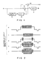
- Fig. 1 shows a conventional video signal processing circuit for separating and extracting two types of signals from an input video signal. Fig. 2 shows signal waveforms of the main part of the circuit shown in Fig. 1. An input video signal A is simultaneously supplied to an adding
circuit 32 and asubtracting circuit 33 in addition to adelay element 31. Thedelay element 31 delays the input video signal A including a luminance signal and a chrominance signal by a 1H period and outputs a 1H-delayed signal. This delayed output signal B is supplied to a band-pass filter (referred to as a BPF hereinafter) 34. TheBPF 34 eliminates a DC component from the delayed output signal B from thedelay element 31 to extract 1H-preceding chrominance signal C. The extracted 1H-preceding chrominance signal C is simultaneously supplied to the addingcircuit 32 and thesubtracting circuit 33. The addingcircuit 32 extracts a luminance signal D by adding the original input video signal A and the 1H-preceding chrominance signal C. Meanwhile, thesubtracting circuit 33 extracts chrominance signal E including a luminance signal by subtracting the 1H-preceding chrominance signal C from the original input video signal A. The chrominance signal E including the luminance signal is supplied to aBPF 35 and chrominance signal F is extracted by theBPF 35 from the chrominance signal E. - In the video signal processing circuit with such an arrangement, the output from the
delay element 31 passes through theBPF 34. As a result, comb characteristics of the adding and subtracting circuits are limited to the band of theBPF 34, and the comb characteristics do not influence a low-frequency component of a luminance signal. Therefore, degradation of a vertical resolution can be prevented. - In the conventional circuit described above, however, since the signal delayed by the
delay element 31 is added to or subtracted from the original input video signal, as shown in Fig. 2, chrominance signal components undesirably appear at a non-correlation portion of the luminance signal D. In addition, chrominance signal components undesirably appear at an achromatic portion in the chrominance signal F, or an amplitude of this portion of the chrominance signal is reduced into a half to be -6 dB, resulting in inconvenience. Particularly, in case of chrominance signal, upon Y/C separation in recording, if a color appears at an achromatic portion, since chrominance signal always pass through the comb filter circuit in a chrominance signal processing circuit of a VTR upon playback, a color appears at an achromatic portion. Therefore, a so-called color ghost appears to form an image having poor quality. - It is, therefore, an object of the present invention to provide a video signal processing circuit capable of reducing a color ghost and preventing a luminance signal from leaking into a chrominance signal while keeping degradation of a vertical resolution at a conventional level.
- According to the present invention, there is provided a video signal processing circuit comprising delay means for receiving an input video signal including a luminance signal and a chrominance signal, and delaying the input video signal by a 1H period, a first band-pass filter for receiving an output from the delay means, subtracting means for subtracting an output from the first band-pass filter from the input video signal, attenuating means for attenuating an output from the subtracting means, adding means for adding the output from the first band-pass filter to the input video signal, signal eliminating means for eliminating a frequency component corresponding to the chrominance signal from an output from the adding means, switching signal generating means for generating as a switching signal a signal corresponding to a period corresponding to an amplitude difference in the chrominance signal between the input video signal delayed by a 1H period by the delay means and the input video signal before delay, first switching means for switching and outputting the outputs from the adding means and the signal eliminating means in response to the switching signal from the switching signal generating means, second switching means for switching and outputting the input video signal and an output from the attenuating means in response to the switching signal from the switching signal generating means, and a second band-pass filter for receiving an output from the second switching means.
- This invention can be more fully understood from the following detailed description when taken in conjunction with the accompanying drawings, in which:
- Fig. 1 is a block diagram of a conventional circuit;
- Fig. 2 is a timing chart showing waveforms of signals of the main part of the circuit shown in Fig. 1;
- Fig. 3 is a block diagram showing an arrangement of a circuit of an embodiment according to the present invention; and
- Fig. 4 is a timing chart showing waveforms of signals of the main part of the circuit shown in Fig. 3.
- Referring to Fig. 3, an input video signal A is simultaneously supplied to an adding
circuit 12 and a subtractingcircuit 13 in addition to a delay element 11. The delay element 11 delays the input video signal A including a luminance signal and a chrominance signal by a 1H period and outputs a 1H-delayed signal. This delayed output signal B is supplied to a BPF (band-pass filter) 14. TheBPF 14 eliminates a DC component from the delayed output signal B from the delay element 11 to extract 1H-preceding chrominance signal C. The extracted 1H-preceding chrominance signal C is simultaneously supplied to the addingcircuit 12 and thesubtracting circuit 13. - The adding
circuit 12 generates a luminance signal D by adding the original input video signal A and the 1H-preceding chrominance signal C. The luminance signal D is simultaneously supplied to a trap circuit (TRAP) 15 and afirst switching circuit 16. Thetrap circuit 15 eliminates chrominance signal components having a center frequency of, e.g., 3.58 MHz from the luminance signal D generated by the addingcircuit 12. An output from thetrap circuit 15 is supplied to thefirst switching circuit 16. Thefirst switching circuit 16 outputs a luminance signal E by switching the two input signals in response to a switching signal M to be described later. - Meanwhile, the subtracting
circuit 13 generates a chrominance signal F including a luminance signal by subtracting the 1H-preceding chrominance signal C from the original input video signal A. The chrominance signal F including the luminance signal is supplied to anattenuating circuit 17 for attenuating a signal by -6 dB and amplitudes of the chrominance signal F is attenuated into halves. An output signal from theattenuating circuit 17 and the original video input signal A are simultaneously supplied to asecond switching circuit 18. Thesecond switching circuit 18 switches and outputs the input signals in response to a switching signal M to be described later. An output from thesecond switching circuit 18 is supplied to aBPF 19, and chrominance signal G is extracted by theBPF 19. - On the other hand, referring to Fig. 3,
reference numeral 20 denotes a switching signal generating circuit for generating the switching signal M used in the twoswitching circuits circuit 20 is constituted by aBPF 21, full-wave rectifyingcircuits circuits circuit 26. The input video signal A is supplied to theBPF 21. As in theBPF 14, theBPF 21 eliminates a DC component from the input video signal A to supply an output signal H to the one full-wave rectifyingcircuit 22. In addition, the output signal C from theBPF 14 is supplied to the other full-wave rectifyingcircuit 23. The two full-wave rectifyingcircuits BPFs circuits circuits integrating circuits circuits circuit 26. The comparingcircuit 26 generates the signal M of "H" level when a predetermined potential difference between the integrated output signals K and L from theintegrating circuits signal generating circuit 20 generates as a switching signal M a signal corresponding to a period corresponding to the amplitude difference in the chrominance signal between the input video signal delayed by a 1H period by the delay element 11 and the input video signal before delay. - The operation of the circuit with this arrangement will be described with reference to a timing chart of waveforms shown in Fig. 4.
- As shown in Fig. 4, when the input video signal A including a luminance signal and a chrominance signal is supplied to the delaying element 11, a signal B is output from the delay element 11. In the
BPF 14 for receiving the signal B, a DC component is eliminated from the signal B, and the signal C including only chrominance signal components is output, as shown in Fig. 4. In the addingcircuit 12, the signal C is added to the input video signal A. Phase of chrominance signal of the input video signal A is different from these of the 1H-preceding signal B by 180°. Therefore, in the output signal D from the addingcircuit 12, there is no chrominance signal component at a portion where the chrominance signal components are included in both the corresponding portions of the signals A and B, and there are chrominance signal components at positions where only one of the corresponding portions of the signals A and B includes the chrominance signal components. - Meanwhile, since the output signal C from the
BPF 14 is also supplied to thesubtracting circuit 13, the signal C is subtracted from the input video signal A by thesubtracting circuit 13. In the output signal F from thesubtracting circuit 13, there are chrominance signal components each having an amplitude twice the original amplitude at a portion where the chrominance signal components are included in both the signals A and B, and there are chrominance signal components each having the original amplitude at a portion where only one of the signals A and B includes chrominance signal components. An output signal from thesubtracting circuit 13 is attenuated by theattenuating circuit 17 to be a signal having an amplitude half the original amplitude. - Meanwhile, in the switching
signal generating circuit 20, as shown in Fig. 4, a signal H including only chrominance signal components is output from theBPF 21 to which the input video signal A is supplied. In the full-wave rectifyingcircuits BPF 14, the input signals are respectively full-wave rectified, and the signals I and H as shown in Fig. 4 are respectively output. Both the output signals I and J are respectively integrated by the integratingcircuits circuit 26 generates the switching signal M of "H" level when a predetermined potential difference between the outputs from theintegrating circuits - In the
first switching circuit 16, when the switching signal M is at "L" level, the output from the addingcircuit 12 is selected, and when the switching signal M is at "H" level, the output from thetrap circuit 15 is selected. As a result, when the signal D (output signal from the adding circuit 12) shown in Fig. 4 does not include chrominance signal components, the signal D is selected. When the signal D includes chrominance signal components, the signal D having passed through thetrap circuit 15 to eliminate the chrominance signal components is selected. Therefore, a luminance signal E without chrominance signal components is output from thefirst switching circuit 16. - In the
second switching circuit 18, when the switching signal M is at "L" level, the output from the attenuatingcircuit 17 is selected, and when the signal M is at "H" level, the input video signal A is selected. As a result, a signal including chrominance signal components having the original amplitude at the same portion as the original input video signal A is output from thesecond switching circuit 18. A DC component is eliminated from the output signal from thesecond switching circuit 18 by passing this output signal through theBPF 19. Therefore, chrominance signal G always have a predetermined amplitude, and never include chrominance signal components at the achromatic portion. - As described above, in the circuit of this embodiment, since the output from the delay element basically passes through the BPF, degradation of a vertical resolution can be kept at the conventional level. In addition, according to the circuit of this embodiment, chrominance signal components never appear at the achromatic portion, and the amplitudes of the chrominance signal of this portion are never reduced into a half to be -6 dB. As a result, upon Y/C separation in recording, no color appears at an achromatic portion. Therefore, in playback, when chrominance signal pass through a comb filter circuit in chrominance signal processing circuit of a VTR, no color appears at an achromatic portion. As a result, a so-called color ghost can be prevented.
- The present invention is not limited to the above embodiment, and it is obvious that the various modifications can be made. For example, in the above embodiment, the switching
signal generating circuit 20 is arranged as shown in Fig. 3. However, another circuit having a function of generating as a switching signal a signal corresponding to a period corresponding to an amplitude difference in the chrominance signal between the input video signal delayed by a 1H period by the delay element and the input video signal before delay may be used. - As described above, according to the present invention, a color ghost can be reduced and a luminance signal can be prevented from leaking into a chrominance signal while the degradation of the vertical resolution is kept at the conventional level.
- Reference signs in the claims are intended for better understanding and shall not limit the scope.
Claims (5)
delay means (11) for receiving an input video signal including a luminance signal and a chrominance signal to delay said input video signal by a one-horizontal period;
a first band-pass filter (14) for receiving an output from said delay means;
subtracting means (13) for subtracting an output from said first band-pass filter from said input video signal;
attenuating means (17) for attenuating an output from said subtracting means;
adding means (12) for adding said output from said first band-pass filter to said input video signal;
signal eliminating means (15) for eliminating a frequency component corresponding to said chrominance signal from an output from said adding means;
switching signal generating means (20) for generating as a switching signal a signal corresponding to a period corresponding to an amplitude difference in said chrominance signal between said input video signal delayed by one horizontal period by said delay means and said input video signal before delay;
first switching means (16) for switching and outputting outputs from said adding means and said signal eliminating means in response to said switching signal from said switching signal generating means;
second switching means (18) for switching and outputting said input video signal and an output from said attenuating means in response to said switching signal from said switching signal generating means; and
a second band-pass filter (19) for receiving an output from said second switching means (18).
a second band-pass filter (21) for receiving said input video signal;
first rectifying means (22) for rectifying said output from said first band-pass filter;
second rectifying means (23) for rectifying an output from said second band-pass filter;
first integrating means (24) for integrating an output from said first rectifying means;
second integrating means (25) for integrating an output from said second rectifying means; and
comparing means (26) for receiving outputs from said first integrating means and said second integrating means, and for generating a signal corresponding to a period during which a predetermined potential is obtained from only one of the outputs from said first and second integrating means.
delay means (11) for receiving an input video signal including a luminance signal and a chrominance signal to delay said input video signal by a onehorizontal period;
a first band-pass filter (14) for receiving an output from said delay means;
subtracting means (13) for subtracting an output from said first band-pass filter from said input video signal;
attenuating means (17) for attenuating an output from said subtracting means;
adding means (12) for adding said output from said first band-pass filter to said input video signal;
signal eliminating means (15) for eliminating a frequency component corresponding to said chrominance signal from an output from said adding means;
a second band-pass filter (21) for receiving said input video signal;
first rectifying means (22) for rectifying an output from said second band-pass filter;
second rectifying means (23) for rectifying said output from said first band-pass filter;
first integrating means (24) for integrating an output from said first rectifying means;
second integrating means (25) for integrating an output from said second rectifying means;
comparing means (26) for receiving outputs from said first integrating means and said second integrating means, and for generating a signal corresponding to a period during which a predetermined potential is obtained from only one of said outputs from said first integrating means and said second integrating means;
first switching means (16) for switching and outputting outputs from said adding means and said signal eliminating means in response to an output from said comparing means;
second switching means (18) for switching and outputting said input video signal and an output from said attenuating means in response to said output from said comparing means; and
a third band-pass filter (19) for receiving an output from said second switching means (18).
Applications Claiming Priority (2)
| Application Number | Priority Date | Filing Date | Title |
|---|---|---|---|
| JP249075/89 | 1989-09-27 | ||
| JP1249075A JPH03112288A (en) | 1989-09-27 | 1989-09-27 | Video signal processing circuit |
Publications (3)
| Publication Number | Publication Date |
|---|---|
| EP0420184A2 true EP0420184A2 (en) | 1991-04-03 |
| EP0420184A3 EP0420184A3 (en) | 1992-06-03 |
| EP0420184B1 EP0420184B1 (en) | 1996-12-11 |
Family
ID=17187634
Family Applications (1)
| Application Number | Title | Priority Date | Filing Date |
|---|---|---|---|
| EP90118466A Expired - Lifetime EP0420184B1 (en) | 1989-09-27 | 1990-09-26 | Video signal processing circuit |
Country Status (5)
| Country | Link |
|---|---|
| US (1) | US5122867A (en) |
| EP (1) | EP0420184B1 (en) |
| JP (1) | JPH03112288A (en) |
| KR (1) | KR930009194B1 (en) |
| DE (1) | DE69029355T2 (en) |
Families Citing this family (1)
| Publication number | Priority date | Publication date | Assignee | Title |
|---|---|---|---|---|
| DE3836043A1 (en) * | 1988-10-20 | 1990-04-26 | Thomson Brandt Gmbh | CIRCUIT FOR AN ADAPTIVE COMB FILTER FOR THE SEPARATION OF LUMINOUSITY SIGNAL AND COLOR TYPE SIGNAL OF AN FBAS-PAL SIGNAL |
Family Cites Families (10)
| Publication number | Priority date | Publication date | Assignee | Title |
|---|---|---|---|---|
| GB1431378A (en) * | 1972-04-19 | 1976-04-07 | Rca Corp | Colour information translating systems |
| US4072984A (en) * | 1975-04-14 | 1978-02-07 | Thomson-Csf Laboratories, Inc. | Chrominance-luminance separator |
| US4050084A (en) * | 1976-07-14 | 1977-09-20 | Cbs Inc. | Comb filter for television signals having adaptive features |
| JPS55150688A (en) * | 1979-05-15 | 1980-11-22 | Sony Corp | Separating circuit of color video signal |
| JPH084347B2 (en) * | 1987-01-28 | 1996-01-17 | 松下電器産業株式会社 | Separator for composite video signal |
| JPH0714220B2 (en) * | 1987-06-12 | 1995-02-15 | パイオニア株式会社 | Y / C separation circuit |
| US4809060A (en) * | 1987-09-10 | 1989-02-28 | Rca Licensing Corporation | Hanging dot reduction arrangement |
| JPH0198385A (en) * | 1987-10-09 | 1989-04-17 | Sony Corp | Correlation detection system |
| US5025311A (en) * | 1987-12-28 | 1991-06-18 | Matsushita Electric Industrial Co., Ltd. | Video signal separating apparatus |
| US4845547A (en) * | 1988-03-28 | 1989-07-04 | North American Philips Corporation | Non-linear comb filter for color TV receivers |
-
1989
- 1989-09-27 JP JP1249075A patent/JPH03112288A/en active Pending
-
1990
- 1990-09-21 US US07/586,219 patent/US5122867A/en not_active Expired - Lifetime
- 1990-09-25 KR KR1019900015170A patent/KR930009194B1/en not_active Expired - Fee Related
- 1990-09-26 DE DE69029355T patent/DE69029355T2/en not_active Expired - Fee Related
- 1990-09-26 EP EP90118466A patent/EP0420184B1/en not_active Expired - Lifetime
Also Published As
| Publication number | Publication date |
|---|---|
| KR930009194B1 (en) | 1993-09-23 |
| KR910007376A (en) | 1991-04-30 |
| DE69029355D1 (en) | 1997-01-23 |
| EP0420184A3 (en) | 1992-06-03 |
| US5122867A (en) | 1992-06-16 |
| EP0420184B1 (en) | 1996-12-11 |
| DE69029355T2 (en) | 1997-04-30 |
| JPH03112288A (en) | 1991-05-13 |
Similar Documents
| Publication | Publication Date | Title |
|---|---|---|
| CA1062361A (en) | Chrominance-luninance separator | |
| US4178609A (en) | Comb filter having improved luminance response | |
| GB2104338A (en) | Noise reduction circuit for a video signal | |
| EP0173439B1 (en) | Luminance/chrominance separator | |
| EP0618738B1 (en) | Comb filter capable of reducing cross-color phenomena and noises | |
| JPH03239087A (en) | Y/c separator | |
| US5047840A (en) | Luminance signal/chrominance signal separating circuit and a noise reduction circuit using a 3 line logical comb filter | |
| KR930006540B1 (en) | Wideband VCR with Comb Filter Suppression Circuit | |
| EP0420184A2 (en) | Video signal processing circuit | |
| CA2016444C (en) | Luminance signal/color signal separating circuit and noise reduction circuit using a comb filter | |
| EP0241935B1 (en) | Color video signal processing circuits | |
| CA1269449A (en) | Comb filter "hanging dot" eliminator | |
| US5014118A (en) | Luminance signal processing circuit using 3 line logical comb filter | |
| JP3428148B2 (en) | Filter circuit | |
| CA1303212C (en) | Signal combining circuitry | |
| EP0444838B1 (en) | Video signal reproducing apparatus | |
| US5309226A (en) | Means for cancelling ghost signals in response to the reception of a non-standard television video signal | |
| JP2698637B2 (en) | Luminance signal / chrominance signal separation circuit | |
| JP3507987B2 (en) | Video signal processing circuit | |
| JP3427271B2 (en) | Video signal processing circuit | |
| JP2609657B2 (en) | Television receiver | |
| Owashi et al. | An integrated digital Y/C separator for S-VHS VCR | |
| GB2221592A (en) | Playback color processing circuit | |
| JPH0345086A (en) | Video signal processing circuit | |
| EP0722254A2 (en) | Delay time compensating apparatus for PAL plus video cassette tape recorder |
Legal Events
| Date | Code | Title | Description |
|---|---|---|---|
| PUAI | Public reference made under article 153(3) epc to a published international application that has entered the european phase |
Free format text: ORIGINAL CODE: 0009012 |
|
| 17P | Request for examination filed |
Effective date: 19900926 |
|
| AK | Designated contracting states |
Kind code of ref document: A2 Designated state(s): DE FR GB |
|
| PUAL | Search report despatched |
Free format text: ORIGINAL CODE: 0009013 |
|
| AK | Designated contracting states |
Kind code of ref document: A3 Designated state(s): DE FR GB |
|
| 17Q | First examination report despatched |
Effective date: 19940518 |
|
| GRAG | Despatch of communication of intention to grant |
Free format text: ORIGINAL CODE: EPIDOS AGRA |
|
| GRAH | Despatch of communication of intention to grant a patent |
Free format text: ORIGINAL CODE: EPIDOS IGRA |
|
| GRAH | Despatch of communication of intention to grant a patent |
Free format text: ORIGINAL CODE: EPIDOS IGRA |
|
| GRAA | (expected) grant |
Free format text: ORIGINAL CODE: 0009210 |
|
| AK | Designated contracting states |
Kind code of ref document: B1 Designated state(s): DE FR GB |
|
| REF | Corresponds to: |
Ref document number: 69029355 Country of ref document: DE Date of ref document: 19970123 |
|
| ET | Fr: translation filed | ||
| PGFP | Annual fee paid to national office [announced via postgrant information from national office to epo] |
Ref country code: FR Payment date: 19970909 Year of fee payment: 8 |
|
| PGFP | Annual fee paid to national office [announced via postgrant information from national office to epo] |
Ref country code: DE Payment date: 19971010 Year of fee payment: 8 |
|
| PLBE | No opposition filed within time limit |
Free format text: ORIGINAL CODE: 0009261 |
|
| STAA | Information on the status of an ep patent application or granted ep patent |
Free format text: STATUS: NO OPPOSITION FILED WITHIN TIME LIMIT |
|
| 26N | No opposition filed | ||
| REG | Reference to a national code |
Ref country code: GB Ref legal event code: 746 Effective date: 19980915 |
|
| PG25 | Lapsed in a contracting state [announced via postgrant information from national office to epo] |
Ref country code: FR Free format text: LAPSE BECAUSE OF NON-PAYMENT OF DUE FEES Effective date: 19990531 |
|
| PG25 | Lapsed in a contracting state [announced via postgrant information from national office to epo] |
Ref country code: DE Free format text: LAPSE BECAUSE OF NON-PAYMENT OF DUE FEES Effective date: 19990701 |
|
| REG | Reference to a national code |
Ref country code: FR Ref legal event code: ST |
|
| REG | Reference to a national code |
Ref country code: GB Ref legal event code: IF02 |
|
| PGFP | Annual fee paid to national office [announced via postgrant information from national office to epo] |
Ref country code: GB Payment date: 20070926 Year of fee payment: 18 |
|
| GBPC | Gb: european patent ceased through non-payment of renewal fee |
Effective date: 20080926 |
|
| PG25 | Lapsed in a contracting state [announced via postgrant information from national office to epo] |
Ref country code: GB Free format text: LAPSE BECAUSE OF NON-PAYMENT OF DUE FEES Effective date: 20080926 |