EP0417681A1 - Zweimodem-Synchronisationseinrichtung, insbesondere für die Rückgewinnung der Rahmentaktphase in einem Halbduplex-Übertragungssystem - Google Patents
Zweimodem-Synchronisationseinrichtung, insbesondere für die Rückgewinnung der Rahmentaktphase in einem Halbduplex-Übertragungssystem Download PDFInfo
- Publication number
- EP0417681A1 EP0417681A1 EP90117357A EP90117357A EP0417681A1 EP 0417681 A1 EP0417681 A1 EP 0417681A1 EP 90117357 A EP90117357 A EP 90117357A EP 90117357 A EP90117357 A EP 90117357A EP 0417681 A1 EP0417681 A1 EP 0417681A1
- Authority
- EP
- European Patent Office
- Prior art keywords
- phase
- frame
- information
- signal
- synchronization
- Prior art date
- Legal status (The legal status is an assumption and is not a legal conclusion. Google has not performed a legal analysis and makes no representation as to the accuracy of the status listed.)
- Granted
Links
Images


Classifications
-
- H—ELECTRICITY
- H04—ELECTRIC COMMUNICATION TECHNIQUE
- H04L—TRANSMISSION OF DIGITAL INFORMATION, e.g. TELEGRAPHIC COMMUNICATION
- H04L7/00—Arrangements for synchronising receiver with transmitter
- H04L7/04—Speed or phase control by synchronisation signals
- H04L7/08—Speed or phase control by synchronisation signals the synchronisation signals recurring cyclically
-
- H—ELECTRICITY
- H04—ELECTRIC COMMUNICATION TECHNIQUE
- H04L—TRANSMISSION OF DIGITAL INFORMATION, e.g. TELEGRAPHIC COMMUNICATION
- H04L7/00—Arrangements for synchronising receiver with transmitter
- H04L7/02—Speed or phase control by the received code signals, the signals containing no special synchronisation information
- H04L7/033—Speed or phase control by the received code signals, the signals containing no special synchronisation information using the transitions of the received signal to control the phase of the synchronising-signal-generating means, e.g. using a phase-locked loop
Definitions
- the field of the invention is that of phase recovery devices, intended to equip a receiver, in a digital transmission system.
- the invention was more particularly developed within the framework of a digital altemat transmission system, in which a receiver receives a frame only at regular intervals, which requires recovering the phase of a local clock at the frame frequency, the period of which is an important multiple of the period of the local bit clock.
- the known solutions generally consist in performing synchronization on the basis of the detection of the first bit of each frame received, or else by the detection of a specific pattern of frame synchronization.
- This pattern can for example consist of a violation of the code used for the transmission of the signal.
- the principle of detection of the first bit of frame received has the disadvantage of having a high sensitivity to noise.
- the need to use a specific synchronization pattern constitutes a penalty as regards the bit rate and the additional relative complexity of the transmission reception systems.
- the objective of the invention is to overcome these drawbacks of existing systems.
- a first objective of the invention is to provide a synchronization system, in particular for the frame synchronization of a receiver receiving frames at regular intervals, which is simple to implement, and which has high immunity against noise, while offering a high sensitivity for hooking the frame frequency.
- Another object of the invention is to provide such a synchronization device which makes it possible, at least for certain types of expression code of the transmitted signal, to avoid using a specific synchronization pattern in the signal transmitted.
- a complementary objective of the invention is to provide a synchronization system providing an indication of relevant phase shift, usable for example to perform phase cortection in a phase locked loop, external to the device of the invention.
- the phase lock loop can, for example, be of the type protected by a joint patent application in the name of the same applicants, under the title "quick lock phase lock loop, in particular for a digital transmission system using alternat ".
- a synchronization device in particular for the synchronization recovery of the phase of the local frame clock of a receiver, in the case of a digital signal formed by frames received at regular intervals, said signal being coded according to a code having a detectable online pulse density
- device characterized in that it comprises: - first phase hooking means, delivering phase shift information between the local clock and the received signal, upon detection of the online presence of said coded signal.
- - second phase recovery means delivering phase shift information between the local clock and the received signal, when a phase reference point of the frames received is detected within a time window centered on the phase of the local clock.
- the synchronization device of the invention has a double mode: - a first mode is used to reach the synchronization state based on an online energy detector. This mode is used at system initialization, as well as at each occurrence of a synchronization stall. - the other mode is used as soon as the synchronization state is reached. Because it is based on a simple time window of a phase reference point of the received frames, it has a lower sensitivity to noise than that of the latching mode.
- the expression code of the transmitted signal is of the WAL2 code type, said reference point of the received frame being formed by the first zero crossing of each frame.
- WAL2 code type WAL2 code type
- other modes or codes of signal transmission can be used, associated with different frame reference points.
- the means for delivering said binary synchronization locking information consist of a tilting system whose first state selects the phase information delivered by the phase hooking means, and the second state selects the phase information delivered by said second phase recovery means, said tilting system being activated by: - first means for forcing said first state, during a confirmation of absence of the phase reference point of the frame received in said time window for N consecutive frames. - second means for forcing said second state, upon confirmation of the presence of the phase reference point of the frame received in said time window for M consecutive frames.
- said first second forcing means consist of counters selectively activated and initialized as a function of said information delivered by said first latching means and second phase recovery means.
- the synchronization system described below has been designed for a two-wire alternation transmission system.
- the transmission is carried out according to a specific code of the type of the WAL2 code.
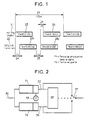
- An alternating transmission system sends and receives data frames according to the diagram in FIG. 1.
- line 21 corresponds to the activity of the master terminal, and line 22 to that of the slave terminal of such a line.
- the master terminal is for example a PABX.
- the master 21 sends a data frame 23 1 to the slave terminal 22. After the propagation time TP 24 in the cable, this frame 23 2 is received by the slave 22.
- Slave 22 waits a certain time to allow the signal to be damped online (guard time 25) before proceeding to send a frame 26 2 to master 21.
- the rate of exchange of the frames is controlled by the master 21 which, in the specific case presented here, sends a frame according to a time period 27 of 125 ⁇ S.
- a bit clock and a frame clock must be recovered to decode the data received by the master 21 and by the slave 22, and also to ensure the good rate of the frames transmitted by the slave.
- synchronization is carried out by the phase comparison between a single reference point contained in the received frame, with a clock for reference to the frame frequency generated by the local clock industry.
- phase comparator which provides information about advance, delay, or even phase coincidence. This information can be used to correct the phase difference detected, in a system external to the device of the invention (see for example the above-mentioned joint patent application).
- the online code used is the WAL2 code.
- This code has the following characteristics: - each symbol transmitted contains energy; - the optimal detection threshold of the signal reception comparator is 0 volts; - each symbol has a passage through 0 volts.
- biphase code has these same characteristics, and therefore also does not require the use of a specific synchronization mode.
- the device of the invention is nevertheless compatible with other codes, such as the AMI code, by adding at least one synchronization symbol in each frame.
- the device of the invention is a double system which reduces the susceptibility to noise and allows detection of a loss of locking by comparing the information provided by the two phase recovery modes.
- the reference point of the received frame in the specific case of the WAL2 code, is the first zero crossing of the frame. With the WAL2 code, this reference point is always in the same place in the frame regardless of the data transmitted.
- a first phase comparator 31 detects the start of each frame of the received signal 30 by detecting the level of the signal online. With the WAL2 code, each bit received contains energy. If the frame is not received, there is a time without energy online.
- the “start of frame” information provided by the energy detector 31 is used to select, from all the zero crossings, the first of the frame received. This zero crossing is then compared in phase with the reference clock 33 delivered by the local clock industry to give information 32 of phase advance or delay.
- phase comparator 34 selects the zero crossing which falls in a window placed around the reference point of the local clock, to provide a phase comparison information 36, independently of the zero crossing selected by the energy detector 31 .
- the windowing phase recovery mode 34 is less sensitive to noise than that 31 operating by energy detection, but it can only be used when the locking is achieved since it cannot distinguish the first passage by zero. other zero crossings contained in the received frame.
- FIG. 3 presents a detailed embodiment of a device operating according to the principle illustrated in FIG. 2.
- FIG. 4 represents the synchronization of the main signals of the circuit of FIG. 3, when the clock local frame is in synchronized state.
- the comparator 101 detects the zero volt passages of the received signal 100. In this specific case of the circuit shown, only the falling edge passages (+ to -) are detected, the first bit of the frame being always a zero binary.
- the output of this comparator 101 samples the reference clock 8KREF 102 in the flip-flop 103.
- the frame clock 8KREF 102 is generated by the local clock and is synchronous with the bit and frame clocks recovered.
- the signal 8KE 104 is set to zero. If it is late, signal 8KE 104 is set to one. The signal 8KE 104 therefore indicates the phase of each zero crossing with respect to the rising edge of 8KREF 102.
- the information of the phase of the first zero crossing of the frame is selected by the flip-flop 105. This flip-flop 105 is triggered by the rising edge of the LED signal 106.
- the comparator 107 detects the energy of the frame received. In a specific embodiment, this comparator 107 has a detection threshold of - 85mV.
- the output of comparator 107 is filtered in a filter module 108. A certain period is counted without energy followed by a certain period with energy before the signal DE 109 passes to one at the output of the filter module 108.
- the rising edge of DE 109 triggers the R / S flip-flop 112 formed by the doors 110 and 111.
- the flip-flop 112 is inhibited and reset during the transmission phase by the reset signal RE 114.
- the output of the gate 110 triggers the flip-flop 105 for validate the phase information between the rising edge of 8 KREF 102 and the first zero crossing of the frame.
- the A / RDE signal 113 is therefore the phase information generated by the phase comparator with energy detector.
- the window FEN 115 frames the rising edge of the local clock at the frame frequency 8KREF 102. It has a width such that only one zero crossing can exist in the window at a time. It is, however, wide enough that in the synchronized state the first zero crossing of the frame falls into the window despite the jitter superimposed on the received signal.
- the zero crossings detected at the output of the comparator 101 sample the FEN signal 115.
- the FENE signal 117 from the flip-flop 116 changes to one with the first zero crossing of the frame.
- the rise of the FENE signal 117 samples the signal 8KREF 102 in the flip-flop 119.
- the output 118 of this flip-flop 119 indicates the phase shift between the rising edge of the signal 8KREF 102 and the first zero crossing of the frame.
- the two phase information A / RDE 113 and A / RF 118 form the inputs of the multiplexer 120.
- the control signal (PVT) 121 of the multiplexer selects one or the other of these two signals according to the synchronization state.
- the output 130 of the multiplexer 120 provides advance, delay, or phase coincidence information.
- the two flip-flops 122 and 123 together with the two counters 124, 125 form the synchronization machine 126.
- the CLRN output 133 of flip-flop 122 changes to one if the zero crossing that falls in the window is the first zero crossing of the frame received (zero crossing selected by the energy detector 107).
- the counter 125 of value N is reset to zero and the counter 124 of value M is activated. If the latter counter 124 counts M consecutive frames, or if the first zero crossing of the frame falls in the window, the flip-flop 123 is preselected and it is considered that synchronization has been achieved. If this zero crossing falls outside the window before synchronization is reached, the counter 124 is reset to zero.
- the output 121 of the flip-flop 123 therefore selects, according to the synchronization state, either the phase information 113 coming from the phase comparator with energy detector, or the phase information 118 coming from the phase comparator with window.
- FIG. 4 represents the synchronization of the main signals of the circuit of FIG. 3, in the synchronized state of the device: - the online signal 100. - The detected signals 131, 132, at the output of the comparators 101, 107 respectively. the LED signal 106 for triggering the flip-flop 105. - the reference clock 8KREF 102 at the frame frequency. - The time window signal FEN 115. the signal 8KE 104 indicating the phase of each zero crossing of the received signal 100 with respect to the clock signal 8KREF 102. - the signal A / RDE 113 corresponding to the phase information generated by the phase comparator 101 with energy detector. - the signal FENE 117 from flip-flop 116. - the signal A / RF 118 corresponding to the phase shift between the rising edge of the signal 8KREF 102 and the first zero crossing of the frame. the signal CLRN 130 output from the flip-flop 122 of the synchronization machine 126.
Applications Claiming Priority (2)
| Application Number | Priority Date | Filing Date | Title |
|---|---|---|---|
| FR8911895 | 1989-09-12 | ||
| FR8911895A FR2651941B1 (fr) | 1989-09-12 | 1989-09-12 | Dispositif de synchronisation a deux modes, notamment pour la recuperation de la phase de l'horloge trame dans un systeme de transmission a l'alternat. |
Publications (2)
| Publication Number | Publication Date |
|---|---|
| EP0417681A1 true EP0417681A1 (de) | 1991-03-20 |
| EP0417681B1 EP0417681B1 (de) | 1994-11-02 |
Family
ID=9385354
Family Applications (1)
| Application Number | Title | Priority Date | Filing Date |
|---|---|---|---|
| EP90117357A Expired - Lifetime EP0417681B1 (de) | 1989-09-12 | 1990-09-10 | Zweimodem-Synchronisationseinrichtung, insbesondere für die Rückgewinnung der Rahmentaktphase in einem Halbduplex-Übertragungssystem |
Country Status (7)
| Country | Link |
|---|---|
| US (1) | US5151927A (de) |
| EP (1) | EP0417681B1 (de) |
| AT (1) | ATE113778T1 (de) |
| DE (1) | DE69013832T2 (de) |
| DK (1) | DK0417681T3 (de) |
| ES (1) | ES2064574T3 (de) |
| FR (1) | FR2651941B1 (de) |
Families Citing this family (3)
| Publication number | Priority date | Publication date | Assignee | Title |
|---|---|---|---|---|
| US5959979A (en) * | 1997-05-05 | 1999-09-28 | Northrop Grumman Corporation | Half-duplex communication system for telemetry modems |
| US7237182B1 (en) | 2003-12-12 | 2007-06-26 | Cisco Technology, Inc. | System and method for selectively recovering frames in a communications environment |
| US8154995B2 (en) * | 2005-01-26 | 2012-04-10 | At&T Intellectual Property I, L.P. | System and method of managing digital data transmission |
Citations (2)
| Publication number | Priority date | Publication date | Assignee | Title |
|---|---|---|---|---|
| EP0082575A1 (de) * | 1981-12-21 | 1983-06-29 | Motorola, Inc. | Energiesynchronisierter Demodulatorschaltkreis |
| GB2174871A (en) * | 1985-05-09 | 1986-11-12 | Northern Telecom Ltd | Frame synchronization circuit for digital transmission system |
Family Cites Families (3)
| Publication number | Priority date | Publication date | Assignee | Title |
|---|---|---|---|---|
| US3251034A (en) * | 1962-05-21 | 1966-05-10 | Texas Instruments Inc | Synchronizing system for digital data recovery apparatus |
| US3575554A (en) * | 1968-04-16 | 1971-04-20 | Communications Satellite Corp | Frame synchronizer for a biorthogonal decoder |
| DE3333714A1 (de) * | 1983-09-17 | 1985-04-04 | Standard Elektrik Lorenz Ag, 7000 Stuttgart | Schaltungsanordnung zur rahmen- und phasensynchronisation eines empfangsseitigen abtasttaktes |
-
1989
- 1989-09-12 FR FR8911895A patent/FR2651941B1/fr not_active Expired - Lifetime
-
1990
- 1990-09-10 DE DE69013832T patent/DE69013832T2/de not_active Expired - Fee Related
- 1990-09-10 AT AT90117357T patent/ATE113778T1/de active
- 1990-09-10 EP EP90117357A patent/EP0417681B1/de not_active Expired - Lifetime
- 1990-09-10 DK DK90117357.5T patent/DK0417681T3/da active
- 1990-09-10 ES ES90117357T patent/ES2064574T3/es not_active Expired - Lifetime
- 1990-09-11 US US07/580,733 patent/US5151927A/en not_active Expired - Fee Related
Patent Citations (2)
| Publication number | Priority date | Publication date | Assignee | Title |
|---|---|---|---|---|
| EP0082575A1 (de) * | 1981-12-21 | 1983-06-29 | Motorola, Inc. | Energiesynchronisierter Demodulatorschaltkreis |
| GB2174871A (en) * | 1985-05-09 | 1986-11-12 | Northern Telecom Ltd | Frame synchronization circuit for digital transmission system |
Also Published As
| Publication number | Publication date |
|---|---|
| FR2651941A1 (fr) | 1991-03-15 |
| EP0417681B1 (de) | 1994-11-02 |
| DK0417681T3 (da) | 1995-01-16 |
| ATE113778T1 (de) | 1994-11-15 |
| DE69013832T2 (de) | 1995-03-23 |
| DE69013832D1 (de) | 1994-12-08 |
| ES2064574T3 (es) | 1995-02-01 |
| US5151927A (en) | 1992-09-29 |
| FR2651941B1 (fr) | 1991-10-25 |
Similar Documents
| Publication | Publication Date | Title |
|---|---|---|
| EP0863635B1 (de) | Verfahren und Vorrichtung zur Übertragung von Datenrahmen | |
| FR2748171A1 (fr) | Procede de generation d'un signal d'horloge pour une utilisation dans un recepteur de donnees, generateur d'horloge, recepteur de donnees et systeme d'acces telecommande pour vehicules | |
| FR2526979A1 (fr) | Systeme de detection d'intrusion | |
| FR2473817A1 (fr) | Circuit de detection du decrochage d'une boucle numerique a accrochage de phase | |
| EP0932283B1 (de) | BPSK-Demodulator für ein PCM-Signal | |
| CA1209712A (fr) | Procede et installation de transmission de donnees numeriques | |
| EP0417681B1 (de) | Zweimodem-Synchronisationseinrichtung, insbesondere für die Rückgewinnung der Rahmentaktphase in einem Halbduplex-Übertragungssystem | |
| US3903504A (en) | Binary phase digital decoding system | |
| EP0355073B1 (de) | Verfahren zur Synchronisation und Anordnung zur Synchronisationsrückgewinnung für Übertragung in Zeitgetrenntlage | |
| EP0199294B1 (de) | Verfahren und Anordnung zur Signalisierung über eine bidirektionale digitale Übertragungsstrecke | |
| EP0064923B1 (de) | System zur Phasensynchronisation digitaler Datenströme und seine Verwendung bei der Umschaltung der Datenströme | |
| EP0056748B1 (de) | Verfahren zur empfangsseitigen Synchronisation paketweise übertragener, digitaler Signale | |
| FR2945398A1 (fr) | Demodulateur et systeme de transmission d'informations modulees, notamment pour etiquette d'identification radiofrequence | |
| EP0370862A1 (de) | Verfahren und System zur Signalübertragung | |
| FR2483104A1 (fr) | Dispositif indicateur de zone d'alarme | |
| FR2505584A1 (fr) | Circuit pour reporter des donnees entre deux systemes | |
| CA1236552A (fr) | Procede de telesignalisation pour une liaison de transmission numerique et dispositif pour sa mise en oeuvre | |
| EP0018618B1 (de) | Vorrichtung zur Synchronisierung eines Multiplexers in einer Zeitmultiplex-Vermittlungsstelle | |
| EP0100523B1 (de) | Verfahren zur Informationsübertragung über einen einzigen Übertragungskanal und Anwendung dieses Verfahrens insbesondere in Einrichtungen die ein Alarmsystem bilden | |
| CA1232689A (fr) | Procede et dispositif de detection d'erreur dans un train d'informations binaires exprimees selon le code cmi | |
| FR2640098A1 (fr) | Dispositif de synchronisation de l'emission et de la reception d'une station d'un reseau de communication notamment pour vehicule automobile | |
| FR2526562A1 (fr) | Interrupteur photo-optique de porte | |
| EP0343083A1 (de) | Synchronisationsverlust-Detektionseinrichtung und deren Anwendung in einem Digitalübertragungsnetz | |
| EP0637417B1 (de) | Datenübertragungseinrichtung und verfahren für funknetz | |
| FR2638268A1 (fr) | Dispositifs pour permettre de discriminer entre plusieurs phenomenes simultanes |
Legal Events
| Date | Code | Title | Description |
|---|---|---|---|
| PUAI | Public reference made under article 153(3) epc to a published international application that has entered the european phase |
Free format text: ORIGINAL CODE: 0009012 |
|
| AK | Designated contracting states |
Kind code of ref document: A1 Designated state(s): AT BE CH DE DK ES FR GB IT LI NL SE |
|
| 17P | Request for examination filed |
Effective date: 19910917 |
|
| 17Q | First examination report despatched |
Effective date: 19931108 |
|
| GRAA | (expected) grant |
Free format text: ORIGINAL CODE: 0009210 |
|
| AK | Designated contracting states |
Kind code of ref document: B1 Designated state(s): AT BE CH DE DK ES FR GB IT LI NL SE |
|
| REF | Corresponds to: |
Ref document number: 113778 Country of ref document: AT Date of ref document: 19941115 Kind code of ref document: T |
|
| REF | Corresponds to: |
Ref document number: 69013832 Country of ref document: DE Date of ref document: 19941208 |
|
| GBT | Gb: translation of ep patent filed (gb section 77(6)(a)/1977) |
Effective date: 19941121 |
|
| ITF | It: translation for a ep patent filed |
Owner name: JACOBACCI CASETTA & PERANI S.P.A. |
|
| REG | Reference to a national code |
Ref country code: DK Ref legal event code: T3 |
|
| REG | Reference to a national code |
Ref country code: ES Ref legal event code: FG2A Ref document number: 2064574 Country of ref document: ES Kind code of ref document: T3 |
|
| PLBE | No opposition filed within time limit |
Free format text: ORIGINAL CODE: 0009261 |
|
| STAA | Information on the status of an ep patent application or granted ep patent |
Free format text: STATUS: NO OPPOSITION FILED WITHIN TIME LIMIT |
|
| 26N | No opposition filed | ||
| PGFP | Annual fee paid to national office [announced via postgrant information from national office to epo] |
Ref country code: DK Payment date: 19980824 Year of fee payment: 9 Ref country code: AT Payment date: 19980824 Year of fee payment: 9 |
|
| PGFP | Annual fee paid to national office [announced via postgrant information from national office to epo] |
Ref country code: NL Payment date: 19980827 Year of fee payment: 9 |
|
| PGFP | Annual fee paid to national office [announced via postgrant information from national office to epo] |
Ref country code: BE Payment date: 19980908 Year of fee payment: 9 |
|
| PGFP | Annual fee paid to national office [announced via postgrant information from national office to epo] |
Ref country code: ES Payment date: 19980925 Year of fee payment: 9 |
|
| PGFP | Annual fee paid to national office [announced via postgrant information from national office to epo] |
Ref country code: GB Payment date: 19990813 Year of fee payment: 10 |
|
| PGFP | Annual fee paid to national office [announced via postgrant information from national office to epo] |
Ref country code: CH Payment date: 19990816 Year of fee payment: 10 |
|
| PGFP | Annual fee paid to national office [announced via postgrant information from national office to epo] |
Ref country code: FR Payment date: 19990817 Year of fee payment: 10 |
|
| PGFP | Annual fee paid to national office [announced via postgrant information from national office to epo] |
Ref country code: DE Payment date: 19990820 Year of fee payment: 10 |
|
| PGFP | Annual fee paid to national office [announced via postgrant information from national office to epo] |
Ref country code: SE Payment date: 19990823 Year of fee payment: 10 |
|
| PG25 | Lapsed in a contracting state [announced via postgrant information from national office to epo] |
Ref country code: DK Free format text: LAPSE BECAUSE OF NON-PAYMENT OF DUE FEES Effective date: 19990910 Ref country code: AT Free format text: LAPSE BECAUSE OF NON-PAYMENT OF DUE FEES Effective date: 19990910 |
|
| PG25 | Lapsed in a contracting state [announced via postgrant information from national office to epo] |
Ref country code: ES Free format text: LAPSE BECAUSE OF NON-PAYMENT OF DUE FEES Effective date: 19990911 |
|
| PG25 | Lapsed in a contracting state [announced via postgrant information from national office to epo] |
Ref country code: BE Free format text: LAPSE BECAUSE OF NON-PAYMENT OF DUE FEES Effective date: 19990930 |
|
| BERE | Be: lapsed |
Owner name: ALCATEL BUSINESS SYSTEMS Effective date: 19990930 |
|
| PG25 | Lapsed in a contracting state [announced via postgrant information from national office to epo] |
Ref country code: NL Free format text: LAPSE BECAUSE OF NON-PAYMENT OF DUE FEES Effective date: 20000401 |
|
| NLV4 | Nl: lapsed or anulled due to non-payment of the annual fee |
Effective date: 20000401 |
|
| REG | Reference to a national code |
Ref country code: DK Ref legal event code: EBP |
|
| PG25 | Lapsed in a contracting state [announced via postgrant information from national office to epo] |
Ref country code: GB Free format text: LAPSE BECAUSE OF NON-PAYMENT OF DUE FEES Effective date: 20000910 |
|
| PG25 | Lapsed in a contracting state [announced via postgrant information from national office to epo] |
Ref country code: SE Free format text: THE PATENT HAS BEEN ANNULLED BY A DECISION OF A NATIONAL AUTHORITY Effective date: 20000929 |
|
| PG25 | Lapsed in a contracting state [announced via postgrant information from national office to epo] |
Ref country code: LI Free format text: LAPSE BECAUSE OF NON-PAYMENT OF DUE FEES Effective date: 20000930 Ref country code: CH Free format text: LAPSE BECAUSE OF NON-PAYMENT OF DUE FEES Effective date: 20000930 |
|
| GBPC | Gb: european patent ceased through non-payment of renewal fee |
Effective date: 20000910 |
|
| REG | Reference to a national code |
Ref country code: CH Ref legal event code: PL |
|
| EUG | Se: european patent has lapsed |
Ref document number: 90117357.5 |
|
| PG25 | Lapsed in a contracting state [announced via postgrant information from national office to epo] |
Ref country code: FR Free format text: LAPSE BECAUSE OF NON-PAYMENT OF DUE FEES Effective date: 20010531 |
|
| PG25 | Lapsed in a contracting state [announced via postgrant information from national office to epo] |
Ref country code: DE Free format text: LAPSE BECAUSE OF NON-PAYMENT OF DUE FEES Effective date: 20010601 |
|
| REG | Reference to a national code |
Ref country code: FR Ref legal event code: ST |
|
| REG | Reference to a national code |
Ref country code: ES Ref legal event code: FD2A Effective date: 20001013 |
|
| PG25 | Lapsed in a contracting state [announced via postgrant information from national office to epo] |
Ref country code: IT Free format text: LAPSE BECAUSE OF NON-PAYMENT OF DUE FEES;WARNING: LAPSES OF ITALIAN PATENTS WITH EFFECTIVE DATE BEFORE 2007 MAY HAVE OCCURRED AT ANY TIME BEFORE 2007. THE CORRECT EFFECTIVE DATE MAY BE DIFFERENT FROM THE ONE RECORDED. Effective date: 20050910 |