EP0409328A2 - A switched bridge circuit - Google Patents
A switched bridge circuit Download PDFInfo
- Publication number
- EP0409328A2 EP0409328A2 EP90201903A EP90201903A EP0409328A2 EP 0409328 A2 EP0409328 A2 EP 0409328A2 EP 90201903 A EP90201903 A EP 90201903A EP 90201903 A EP90201903 A EP 90201903A EP 0409328 A2 EP0409328 A2 EP 0409328A2
- Authority
- EP
- European Patent Office
- Prior art keywords
- circuit
- coupled
- transistor
- input
- output
- Prior art date
- Legal status (The legal status is an assumption and is not a legal conclusion. Google has not performed a legal analysis and makes no representation as to the accuracy of the status listed.)
- Granted
Links
Images


Classifications
-
- H—ELECTRICITY
- H03—ELECTRONIC CIRCUITRY
- H03K—PULSE TECHNIQUE
- H03K17/00—Electronic switching or gating, i.e. not by contact-making and –breaking
-
- H—ELECTRICITY
- H02—GENERATION; CONVERSION OR DISTRIBUTION OF ELECTRIC POWER
- H02M—APPARATUS FOR CONVERSION BETWEEN AC AND AC, BETWEEN AC AND DC, OR BETWEEN DC AND DC, AND FOR USE WITH MAINS OR SIMILAR POWER SUPPLY SYSTEMS; CONVERSION OF DC OR AC INPUT POWER INTO SURGE OUTPUT POWER; CONTROL OR REGULATION THEREOF
- H02M1/00—Details of apparatus for conversion
- H02M1/38—Means for preventing simultaneous conduction of switches
-
- H—ELECTRICITY
- H02—GENERATION; CONVERSION OR DISTRIBUTION OF ELECTRIC POWER
- H02H—EMERGENCY PROTECTIVE CIRCUIT ARRANGEMENTS
- H02H7/00—Emergency protective circuit arrangements specially adapted for specific types of electric machines or apparatus or for sectionalised protection of cable or line systems, and effecting automatic switching in the event of an undesired change from normal working conditions
- H02H7/10—Emergency protective circuit arrangements specially adapted for specific types of electric machines or apparatus or for sectionalised protection of cable or line systems, and effecting automatic switching in the event of an undesired change from normal working conditions for converters; for rectifiers
- H02H7/12—Emergency protective circuit arrangements specially adapted for specific types of electric machines or apparatus or for sectionalised protection of cable or line systems, and effecting automatic switching in the event of an undesired change from normal working conditions for converters; for rectifiers for static converters or rectifiers
- H02H7/122—Emergency protective circuit arrangements specially adapted for specific types of electric machines or apparatus or for sectionalised protection of cable or line systems, and effecting automatic switching in the event of an undesired change from normal working conditions for converters; for rectifiers for static converters or rectifiers for inverters, i.e. DC/AC converters
-
- H—ELECTRICITY
- H02—GENERATION; CONVERSION OR DISTRIBUTION OF ELECTRIC POWER
- H02M—APPARATUS FOR CONVERSION BETWEEN AC AND AC, BETWEEN AC AND DC, OR BETWEEN DC AND DC, AND FOR USE WITH MAINS OR SIMILAR POWER SUPPLY SYSTEMS; CONVERSION OF DC OR AC INPUT POWER INTO SURGE OUTPUT POWER; CONTROL OR REGULATION THEREOF
- H02M7/00—Conversion of AC power input into DC power output; Conversion of DC power input into AC power output
- H02M7/42—Conversion of DC power input into AC power output without possibility of reversal
- H02M7/44—Conversion of DC power input into AC power output without possibility of reversal by static converters
- H02M7/48—Conversion of DC power input into AC power output without possibility of reversal by static converters using discharge tubes with control electrode or semiconductor devices with control electrode
- H02M7/53—Conversion of DC power input into AC power output without possibility of reversal by static converters using discharge tubes with control electrode or semiconductor devices with control electrode using devices of a triode or transistor type requiring continuous application of a control signal
- H02M7/537—Conversion of DC power input into AC power output without possibility of reversal by static converters using discharge tubes with control electrode or semiconductor devices with control electrode using devices of a triode or transistor type requiring continuous application of a control signal using semiconductor devices only, e.g. single switched pulse inverters
- H02M7/538—Conversion of DC power input into AC power output without possibility of reversal by static converters using discharge tubes with control electrode or semiconductor devices with control electrode using devices of a triode or transistor type requiring continuous application of a control signal using semiconductor devices only, e.g. single switched pulse inverters in a push-pull configuration
-
- H—ELECTRICITY
- H03—ELECTRONIC CIRCUITRY
- H03K—PULSE TECHNIQUE
- H03K17/00—Electronic switching or gating, i.e. not by contact-making and –breaking
- H03K17/06—Modifications for ensuring a fully conducting state
-
- H—ELECTRICITY
- H03—ELECTRONIC CIRCUITRY
- H03K—PULSE TECHNIQUE
- H03K17/00—Electronic switching or gating, i.e. not by contact-making and –breaking
- H03K17/08—Modifications for protecting switching circuit against overcurrent or overvoltage
- H03K17/082—Modifications for protecting switching circuit against overcurrent or overvoltage by feedback from the output to the control circuit
- H03K17/0822—Modifications for protecting switching circuit against overcurrent or overvoltage by feedback from the output to the control circuit in field-effect transistor switches
-
- H—ELECTRICITY
- H03—ELECTRONIC CIRCUITRY
- H03K—PULSE TECHNIQUE
- H03K17/00—Electronic switching or gating, i.e. not by contact-making and –breaking
- H03K17/51—Electronic switching or gating, i.e. not by contact-making and –breaking characterised by the components used
- H03K17/56—Electronic switching or gating, i.e. not by contact-making and –breaking characterised by the components used by the use, as active elements, of semiconductor devices
- H03K17/687—Electronic switching or gating, i.e. not by contact-making and –breaking characterised by the components used by the use, as active elements, of semiconductor devices the devices being field-effect transistors
- H03K17/6871—Electronic switching or gating, i.e. not by contact-making and –breaking characterised by the components used by the use, as active elements, of semiconductor devices the devices being field-effect transistors the output circuit comprising more than one controlled field-effect transistor
-
- H—ELECTRICITY
- H03—ELECTRONIC CIRCUITRY
- H03K—PULSE TECHNIQUE
- H03K17/00—Electronic switching or gating, i.e. not by contact-making and –breaking
- H03K17/51—Electronic switching or gating, i.e. not by contact-making and –breaking characterised by the components used
- H03K17/56—Electronic switching or gating, i.e. not by contact-making and –breaking characterised by the components used by the use, as active elements, of semiconductor devices
- H03K17/687—Electronic switching or gating, i.e. not by contact-making and –breaking characterised by the components used by the use, as active elements, of semiconductor devices the devices being field-effect transistors
- H03K17/6877—Electronic switching or gating, i.e. not by contact-making and –breaking characterised by the components used by the use, as active elements, of semiconductor devices the devices being field-effect transistors the control circuit comprising active elements different from those used in the output circuit
-
- Y—GENERAL TAGGING OF NEW TECHNOLOGICAL DEVELOPMENTS; GENERAL TAGGING OF CROSS-SECTIONAL TECHNOLOGIES SPANNING OVER SEVERAL SECTIONS OF THE IPC; TECHNICAL SUBJECTS COVERED BY FORMER USPC CROSS-REFERENCE ART COLLECTIONS [XRACs] AND DIGESTS
- Y10—TECHNICAL SUBJECTS COVERED BY FORMER USPC
- Y10S—TECHNICAL SUBJECTS COVERED BY FORMER USPC CROSS-REFERENCE ART COLLECTIONS [XRACs] AND DIGESTS
- Y10S315/00—Electric lamp and discharge devices: systems
- Y10S315/07—Starting and control circuits for gas discharge lamp using transistors
Definitions
- This invention relates to a semiconductor switched bridge circuit having a protection against switching of a semiconductor element on the bridge whilst there is a significant voltage across it.
- a known way of protecting the semiconductor switches of a switched bridge circuit is to compare the output voltage or a proportion of the output with a reference voltage and to feed back the result of this comparison to a control circuit.
- Such an arrangement works satisfactorily but in the case of high voltages such as rectified a.c. mains voltages a high impedance resistor is required to reduce the voltage to a value suitable for comparison in a semiconductor circuit.
- Such resistors are not easy to fabricate as part of an integrated circuit in view of the large surface area required in addition it is necessary to sense when the output is zero and when it is at supply voltage. In addition there are sometimes requirements for more complex controls.
- An oscillator circuit may be connected in circuit to provide the switching signal for effecting commutation.
- the collector of the first and second transistors may be coupled each with their different semiconductor elements in their particular arm of the bridge via a d.c. amplifier.
- the circuit may be conveniently fabricated in a single integrated circuit chip.
- a semiconductor bridge comprises first and second field effect transistors T1 and T2 respectively the drain source paths of which are connected in series between a pair of 300V d.c. supply lines.
- the output from the bridge circuit taken between the source/drain junction of transistors T1 and T2 respectively, feeds a load in the form of a miniature fluorescent lamp 10 via an inductor L and a capacitor C3.
- a capacitor C1 of 220pF is connected across the output of the bridge to reduce the steep edges (300V,30nsecs) to 300V, 300nsec which result when the bridge is controlled by a square wave drive.
- the drive for the bridge is derived from a square wave generator 11 the output of which feeds a control circuit.
- the control circuit comprises a resistor R2 of 39 K.Ohms fed from the generator 11 which resistor is connected to the input of a d.c. amplifier 12 the output of which is coupled with the gate of bridge transistor T2.
- a diode D1 is connected in parallel with the resistor R2.
- the control circuit also comprises a field effect transistor T3 the source of which is coupled via a resistor R3 of 2 K.Ohms to the zero voltage supply line of the circuit and the drain of which is coupled via a resistor R4 of 39 K.Ohms to a +15 volt supply line via a diode D2 and also to the input of a second d.c. amplifier 13 of the control circuit.
- the gate of the transistor T3 is coupled with the generator 11.
- the transistor T3 operates as an inverter and the bridge transistors are caused, by the outputs of the two d.c. amplifierS 12,13 of the control circuit, to conduct alternately in response to the square waveform supplied by the generator.
- the control circuit incorporates a sensing circuit for determining when the rate of change of output voltage from the bridge is zero.
- a sensing circuit for determining when the rate of change of output voltage from the bridge is zero.
- This comprises an npn transistor T4 having its base connected to the bridge output, its emitter connected via a sensing capacitor C2 of 1pF to the emitter of an npn transistor T5 and its collector connector via the 39 K.Ohm resistor R4 to the +15V supply via the diode D2.
- the base of T5 is connected to the OV supply line and a diode D4,D5 is connected between the emitter and base of each of the transistors T4 and T5.
- the complete arrangement 20 can be fabricated as a single integrated chip and can be incorporated in the housing of a miniature fluorescent lamp or luminaire for receiving a fluorescent tube which lamp or luminaire may be adapted for removeable connection to a lamp socket such as is suitable for connection of an incandescent light bulb, e.g. a bayonett or screw fitting, for which it may form a replacement.
- a lamp socket such as is suitable for connection of an incandescent light bulb, e.g. a bayonett or screw fitting, for which it may form a replacement.
- FIG. 3 A refinement of the invention is shown in Figure 3 the circuit of which is similar to Figure 1 and employs the same reference numerals for similar parts.
- a current mirror is formed by two N P N transistors T10 & T11.
- the transistor T10 acts as a clamping diode and has its base and collector electrodes connected together, the base/collector electrodes being connected to the emitter electrode of the transistor T4 and to the base electrode of transistor T11, the emitter electrode of transistor T10 being connected to the output of the bridge and to the emitter of transistor T11.
- the collector electrode of the transistor T11 is connected to the drain electrode of the transistor T3 and to the input of amplifier 13 and to the collector of T4 thereby keeping the voltage low at the input of block 13. This prevents the risk of parasite capacitance to ground at the input to the amplifier 13 from turning on transistor T1 again if low current levels occur in T3.
- a third embodiment of the invention has latches 23′, 22′ which may be substantially similar to 22 & 23 of the previous circuits but with a latching capability.
- the latches 22′, 23′ each have a set and reset input driven by a respective transistor in block 24′ in response to control signals derived from low voltage control part 25′ which is explained in detail in connection with Figures 6 to 8.
- a sensing capacitor C2′ is this time connected between the bridge output and an input to the low voltage control part 25′ which latter is effective to set and reset the latches 23′ & 22′ alternately when there is no current flow in the capacitor C2′ and the bridge output is zero.
- the circuit of Figure 6 and its associated waveform diagrams shown in Figure 7 illustrate one way in which the current through C2′ can be converted into digital signals SSN & SSP which are used in the control of the latches 22′, 23′.
- T22 is switched on, current flowing through R22 causes a switch on voltage to be developed on the base electrode of T21 the current through R22 is limited to V diode/600 ⁇ , where V diode is the base emitter voltage of T21, and excess current flows through T21 to the O volt rail.
- the voltage on the collector electrode of T22 falls and the output SSN is low.
- T23, T24, T25 & T26 are non conductive, the voltage on the collector of T26 is 5V.
- T23 When the bridge output signal goes positive T23 conducts clamping the voltage on the emitter of T23 to 2.V diode being the diode voltages of T23 & T24. Current flow through R23 is limited to V diode/600 ⁇ and excess current flows to the OV rail via T23 & T24. Conduction of T26 results and the current through R24 causes the voltage to fall and the output SSP becomes low. In these circumstances T21 & T22 are non conductive, the voltage on the collector of T22 SSN is high. This operation may be appreciated by reference to the waveform diagrams of Figure 7.
- FIG. 8 there is illustrated a logic circuit, forming part of block 25′ of Figure 5, for providing output on and off pulses to both of the latch circuits 22′, 23′ such that off pulses have preference and have as little as possible delay.
- the generator 11 provides drive pulses G and, via an inverter I31, also drive pulse H.
- inverter I31 also drive pulse H.
- two series inverters I32, I33 and I34, I35 couple the H or G pulses to one input of a four input NAND GATE N1 or N2 thereby introducing delay of the ON pulse.
- each of the NAND gates is coupled via a capacitor resistor differentiating circuit, which converts the output to short pulses, and an inverter I36, I39 to a different one of the drive transistors T15, T18.
- the H & G pulses are also each connected via capacitive resistive differentiating circuits and inverter I37, I38 to a different one of the drive transistors T17, T16 to provide the OFF pulse.
- Alternative circuits then provide an effective differentiating function by converting a step function to a short pulse can be employed instead of a capacitive resistive circuit and such circuits are intended to fall within the term differentiating circuit.
- Examples of such circuits are a monostable multivibrator or a dual input NAND gate having one input fed by the signal direct and the other input fed via a delay circuit e.g. on odd number of inverters.
- the signal occuring between the two inverters I32, I33 and I34, I35 for driving each latch circuit is coupled to an input of the NAND gates N2 and N1 respectively and the signal occuring on the OFF PULSE side prior to the input to inverters I37, I38 is also coupled to another input of the NAND gates N2 and N1 respectively.
- a further input to the NAND gates N1 & N2 is provided from the SSP and SSN outputs of Figure 6 respectively, providing the slew sense signals indicative of whether the output voltage is positive or negative going.
- the inverters I21, I22 can be omitted in which case the N1 input should be connected to the collector electrode of T22 and the N2 input should be connected to the collector electrode of transistor T26.
- FIG. 10 A further refinement of the logic of Figure 8 is shown in Figure 10 where similar parts are given similar reference numerals.
- dual input NAND gates N3 & N4 have been substituted for inverters I37 & I38 the additional input of which is coupled to SSN and SSP respectively.
- the off pulses are continued as long as the bridge output voltage is slewing thereby improving the slew rate insensitivity of the system.
- the elements employed are particularly suitable for fabrication on an integrated circuit chip.
- the entire control circuit may be fabricated as a single integrated circuit chip which may also include the bridge elements and/or the generator 11.
- the switched bridge circuit of this invention has diverse applications for example:- Electronic bridge circuit suitable for providing a primary voltage for ferrite transformers, Control electronics for discrete transistors of high power motors, Shavers, Chargers for batteries e.g. in nickle cadmiun rechargeable devices.
Landscapes
- Engineering & Computer Science (AREA)
- Power Engineering (AREA)
- Inverter Devices (AREA)
- Electronic Switches (AREA)
- Circuit Arrangements For Discharge Lamps (AREA)
- Protection Of Static Devices (AREA)
Abstract
Description
- This invention relates to a semiconductor switched bridge circuit having a protection against switching of a semiconductor element on the bridge whilst there is a significant voltage across it.
- A known way of protecting the semiconductor switches of a switched bridge circuit is to compare the output voltage or a proportion of the output with a reference voltage and to feed back the result of this comparison to a control circuit. Such an arrangement works satisfactorily but in the case of high voltages such as rectified a.c. mains voltages a high impedance resistor is required to reduce the voltage to a value suitable for comparison in a semiconductor circuit. Such resistors are not easy to fabricate as part of an integrated circuit in view of the large surface area required in addition it is necessary to sense when the output is zero and when it is at supply voltage. In addition there are sometimes requirements for more complex controls.
- In bridge circuits such as are used in electronic ballasts for miniature fluorescent lamps driven from a rectified a.c. mains supply, the bridge circuit has to feed an inductive load and very steep voltage surges can appear on the output, for example 300V in 50 n secs, during commutation giving rise to radio interference and additional dissipation because the semiconductor switches cannot turn off sufficiently quickly. One way of reducing this high slew rate is to include a capacitor in parallel with the load which thereby reduces the rate of change of voltage with time. However, this introduces a further problem in that the bridge circuit control can cause destruction of the semiconductor elements in the bridge if switching can occur when there is a significant voltage across them.
- The present invention has resulted from a consideration of this problem and seeks to provide a switched bridge circuit with a control which is switched only when the voltage across the semiconductor element is low. The timing of this is critical and depends on external factors such as the operating frequency and values of non integrable components and the supply voltage.
- According to the invention there is provided a switched bridge circuit in which semiconductor bridge elements are arranged to provide commutated output voltage from a d.c. supply source in response to a switching signal, characterised in that a control circuit for switching the bridge elements is coupled with the output by a capacitor such that switching of the bridge elements is prevented whilst there is a flow of current through the capacitor, which is indicative of changing output voltage.
- The capacitor is effectively monitoring slew rate and , except at start up, if this is 0 as is signified by no current through the capacitor then one of the requirements for permitting switching of the bridge elements that the output voltage is 0 or V supply is met.
- The control circuit may comprise a first transistor which has its base electrode coupled with the output its emitter electrode coupled via said capacitor to the emitter of a second transistor and its collector coupled with one of a pair of d.c. voltage supply lines via a first resistor and to the control electrode of a semiconductor element in one arm of the bridge, and in which the base of the second transistor is coupled to the other of said pair of d.c. supply lines and the collector is coupled with the control electrode of a semiconductor element in the other arm of the bridge, the collector of the first transistor is coupled via the drain/source path of a field effect transistor and a second resistor to said other d.c. supply line, the gate electrode of the field effect transistor is coupled to a switching signal line for receiving said switching signal which line is coupled via a third resistor with the collector of the second transistor.
- An oscillator circuit may be connected in circuit to provide the switching signal for effecting commutation.
- The first and second transistors may each be provided with a diode connected between their base and emitter so as to be reverse biased when the transistor is conductive.
- The collector of the first and second transistors may be coupled each with their different semiconductor elements in their particular arm of the bridge via a d.c. amplifier.
- In an advantageous arrangement the d.c. amplifiers each comprise a fourth transistor of one conductivity type and a fifth transistor of the opposite conductivity type having their bases coupled with the collector of one of the first and second transistors respectively, the emitter electrode of which fourth transistor is coupled to the emitter electrode of the fifth transistor and to the control electrode of the semiconductor element in their particular arm of the bridge and a sixth transistor of said first conductivity type having its base coupled with the collector of the fifth transistor, and its collector emitter path connected in parallel with one of the bridge elements.
- The circuit may be conveniently fabricated in a single integrated circuit chip.
- According to another aspect of the invention there is provided an a.c. powered switched bridge circuit characterised in the combination of a voltage clamp coupled in parallel with a pair of input lines for a source of alternating current supply, a rectifier circuit coupled with the output of the voltage clamp and a switched bridge circuit as previously defined coupled with the output of the rectifier circuit.
- According to a specific application of the invention there is provided a fluorescent lamp unit, characterised in the combination of a fluorescent tube and ballast and an a.c. powered switched bridge circuit as previously defined the bridge circuit of which is configured as a switched mode power converter which feeds the tube.
- The voltage clamp, the rectifier circuit, the switched bridge circuit, the tube and ballast may all be incorporated in a lamp housing or all of these except the tube may be incorporated in a luminaire for receiving a miniature fluorescent tube. The lamp housing or luminaire may be adapted for removeable connection to a lamp socket such as is suitable for connection of an incandescent light bulb.
- In order that the invention and its various other preferred features may be understood more easily, an embodiment thereof will now be described, by way of example only, with reference to the drawings, in which:-
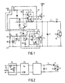
- Figure 1 is a schematic circuit diagram of a switched bridge circuit constructed in accordance with the invention,
- Figure 2 is a partial block schematic diagram of a fluorescent lamp unit incorporating a switched bridge circuit in accordance with the invention,
- Figure 3 is a circuit diagram showing a second embodiment of switched bridge circuit constructed in accordance with the invention,
- Figure 4 is a simplified block schematic drawing showing the basic blocks of Figures 1 & 3,
- Figure 5 is a block schematic drawing showing a third embodiment of switched bridge circuit constructed in accordance with the invention,
- Figure 6 is a detail circuit for converting capacitive current into digital signals which circuit is part of the embodiment of Figure 5,
- Figure 7 is a waveform diagram for illustrating the operation of the circuit of Figure 6,
- Figure 8 is a block schematic diagram showing in more detail part of the embodiment of Figure 5,
- Figure 9 is a waveform diagram for illustrating the operation of the circuit of Figure 8,
- Figure 10 is a block schematic diagram similar to Figure 8 but incorporating a further refinement of the invention.
- In the switched bridge circuit of Figure 1 a semiconductor bridge comprises first and second field effect transistors T1 and T2 respectively the drain source paths of which are connected in series between a pair of 300V d.c. supply lines. In the illustrated example the output from the bridge circuit, taken between the source/drain junction of transistors T1 and T2 respectively, feeds a load in the form of a miniature
fluorescent lamp 10 via an inductor L and a capacitor C3. A capacitor C1 of 220pF is connected across the output of the bridge to reduce the steep edges (300V,30nsecs) to 300V, 300nsec which result when the bridge is controlled by a square wave drive. The drive for the bridge is derived from asquare wave generator 11 the output of which feeds a control circuit. - The control circuit comprises a resistor R2 of 39 K.Ohms fed from the
generator 11 which resistor is connected to the input of a d.c. amplifier 12 the output of which is coupled with the gate of bridge transistor T2. A diode D1 is connected in parallel with the resistor R2. The control circuit also comprises a field effect transistor T3 the source of which is coupled via a resistor R3 of 2 K.Ohms to the zero voltage supply line of the circuit and the drain of which is coupled via a resistor R4 of 39 K.Ohms to a +15 volt supply line via a diode D2 and also to the input of a second d.c.amplifier 13 of the control circuit. The gate of the transistor T3 is coupled with thegenerator 11. The transistor T3 operates as an inverter and the bridge transistors are caused, by the outputs of the two d.c.amplifierS - The control circuit incorporates a sensing circuit for determining when the rate of change of output voltage from the bridge is zero. This comprises an npn transistor T4 having its base connected to the bridge output, its emitter connected via a sensing capacitor C2 of 1pF to the emitter of an npn transistor T5 and its collector connector via the 39 K.Ohm resistor R4 to the +15V supply via the diode D2. The base of T5 is connected to the OV supply line and a diode D4,D5 is connected between the emitter and base of each of the transistors T4 and T5.
- The circuit operation will now be described starting from the instant where bridge transistor T1 is conductive (ON) and T2 and T3 are non conductive (OFF) and the voltage, from the
generator 11, E in = O. The output current to the load is 200 m.Amp. Now E in changes to 15 volts and the voltage V2 between gate and source of transistor T2 starts to rise towards 15 volts with a time constant determined by R2 and the parasitic capacitance of the circuit. T3 is immediately switched on, the voltage drop across R4 becomes 15V so that the voltage input toamplifier 13 and its output is zero. Accordingly the voltage V1 between gate and source of transistor T1 is O. The load discharges C1 and the same voltage appears across C2. Whilst current flows through C2 and through D4 and T5 on providing a zero voltage at the input of theamplifier 12 and V2 becomes O. As soon as the output voltage is equal to O volts the current through C2 becomes zero, V2 becomes 15 volts and T2 is switched on. The current through the load then decreases to - 200 mA, E in becomes O and T2 is switched off. A similar operation occurs for transistor T1, to ensure that this only switches when the voltage is zero, the transistors T1 and T2 being switched alternately. - In this simple way the sensing circuit effectively determines when the output voltage is zero and also determines, from the direction of current flow through it, which of the transistors T1 and T2 is to be switched on. For a load current of 200 mA, a slew rate reduction capacitor C1 of 220 pF and a 1pf sensing capacitor C2 the current through the sensing capacitor is 900µa which is adequate to derive a control voltage.
- The fluorescent lamp unit of Figure 2 incorporates a switched
bridge circuit 20 as described in connection with Figure 1 feeding aminiature fluorescent lamp 10, such as an SL or PL type, via a ballast circuit comprising a shunt capacitor C1 a series inductor L and series capacitor C3. The source of power is derived from the 240V a.c. mains via avoltage clamp 21 comprising a series arrangement of a resistor RD and voltage dependant resistor VDR connected between the mains lines. The output of the voltage clamp developed across VDR is coupled via a filter andrectifier circuit 22 to the switchedbridge circuit 20. Thecomplete arrangement 20 can be fabricated as a single integrated chip and can be incorporated in the housing of a miniature fluorescent lamp or luminaire for receiving a fluorescent tube which lamp or luminaire may be adapted for removeable connection to a lamp socket such as is suitable for connection of an incandescent light bulb, e.g. a bayonett or screw fitting, for which it may form a replacement. - A refinement of the invention is shown in Figure 3 the circuit of which is similar to Figure 1 and employs the same reference numerals for similar parts. Here a current mirror is formed by two N P N transistors T10 & T11. The transistor T10 acts as a clamping diode and has its base and collector electrodes connected together, the base/collector electrodes being connected to the emitter electrode of the transistor T4 and to the base electrode of transistor T11, the emitter electrode of transistor T10 being connected to the output of the bridge and to the emitter of transistor T11. The collector electrode of the transistor T11 is connected to the drain electrode of the transistor T3 and to the input of
amplifier 13 and to the collector of T4 thereby keeping the voltage low at the input ofblock 13. This prevents the risk of parasite capacitance to ground at the input to theamplifier 13 from turning on transistor T1 again if low current levels occur in T3. - The circuits of Figures 1 & 3 have
portions 22 & 23 enclosed in dotted line boxes and a simplified block schematic is illustrated in Figure 4 to aid illustration of some further embodiments of the invention. - Referring now to Figure 5 a third embodiment of the invention has
latches 23′, 22′ which may be substantially similar to 22 & 23 of the previous circuits but with a latching capability. Thelatches 22′, 23′ each have a set and reset input driven by a respective transistor inblock 24′ in response to control signals derived from lowvoltage control part 25′ which is explained in detail in connection with Figures 6 to 8. A sensing capacitor C2′ is this time connected between the bridge output and an input to the lowvoltage control part 25′ which latter is effective to set and reset thelatches 23′ & 22′ alternately when there is no current flow in the capacitor C2′ and the bridge output is zero. In this way the current through C2 (during slewing of the output signal) can be converted into a signal which can delay the turn on pulse of T1, T2 as long as the output is slewing. The manner in which this determination occurs will now be described in connection with Figures 6, 7 & 8. - The circuit of Figure 6 and its associated waveform diagrams shown in Figure 7 illustrate one way in which the current through C2′ can be converted into digital signals SSN & SSP which are used in the control of the
latches 22′, 23′. If we consider a bridge output signal which goes negative, then T22 is switched on, current flowing through R22 causes a switch on voltage to be developed on the base electrode of T21 the current through R22 is limited to V diode/600Ω, where V diode is the base emitter voltage of T21, and excess current flows through T21 to the O volt rail. The voltage on the collector electrode of T22 falls and the output SSN is low. In these circumstances T23, T24, T25 & T26 are non conductive, the voltage on the collector of T26 is 5V. When the bridge output signal goes positive T23 conducts clamping the voltage on the emitter of T23 to 2.V diode being the diode voltages of T23 & T24. Current flow through R23 is limited to V diode/600Ω and excess current flows to the OV rail via T23 & T24. Conduction of T26 results and the current through R24 causes the voltage to fall and the output SSP becomes low. In these circumstances T21 & T22 are non conductive, the voltage on the collector of T22 SSN is high. This operation may be appreciated by reference to the waveform diagrams of Figure 7. - Referring now to Figure 8 there is illustrated a logic circuit, forming part of
block 25′ of Figure 5, for providing output on and off pulses to both of thelatch circuits 22′, 23′ such that off pulses have preference and have as little as possible delay. Thegenerator 11 provides drive pulses G and, via an inverter I31, also drive pulse H. To ensure priority of the OFF pulses and to avoid glitches, two series inverters I32, I33 and I34, I35 couple the H or G pulses to one input of a four input NAND GATE N1 or N2 thereby introducing delay of the ON pulse. The output of each of the NAND gates is coupled via a capacitor resistor differentiating circuit, which converts the output to short pulses, and an inverter I36, I39 to a different one of the drive transistors T15, T18. The H & G pulses are also each connected via capacitive resistive differentiating circuits and inverter I37, I38 to a different one of the drive transistors T17, T16 to provide the OFF pulse. Alternative circuits then provide an effective differentiating function by converting a step function to a short pulse can be employed instead of a capacitive resistive circuit and such circuits are intended to fall within the term differentiating circuit. Examples of such circuits are a monostable multivibrator or a dual input NAND gate having one input fed by the signal direct and the other input fed via a delay circuit e.g. on odd number of inverters. The signal occuring between the two inverters I32, I33 and I34, I35 for driving each latch circuit is coupled to an input of the NAND gates N2 and N1 respectively and the signal occuring on the OFF PULSE side prior to the input to inverters I37, I38 is also coupled to another input of the NAND gates N2 and N1 respectively. These cross connections ensure that the latches are always oppositely controlled such that when one is on the other is off. - A further input to the NAND gates N1 & N2 is provided from the SSP and SSN outputs of Figure 6 respectively, providing the slew sense signals indicative of whether the output voltage is positive or negative going. The inverters I21, I22 can be omitted in which case the N1 input should be connected to the collector electrode of T22 and the N2 input should be connected to the collector electrode of transistor T26.
- The operation of the logic diagram of Figure 8 can be better understood by reference to the waveform diagram of Figure 9.
- A further refinement of the logic of Figure 8 is shown in Figure 10 where similar parts are given similar reference numerals. In this arrangement dual input NAND gates N3 & N4 have been substituted for inverters I37 & I38 the additional input of which is coupled to SSN and SSP respectively. With this arrangement the off pulses are continued as long as the bridge output voltage is slewing thereby improving the slew rate insensitivity of the system.
- The elements employed are particularly suitable for fabrication on an integrated circuit chip. The entire control circuit may be fabricated as a single integrated circuit chip which may also include the bridge elements and/or the
generator 11. - It will be appreciated that although the circuit has been described employing semiconductors of one conductivity type, a similar circuit can be produced employing transistors of the opposite conductivity type without departing from the scope of this invention.
- It will be appreciated that the switched bridge circuit of this invention has diverse applications for example:-
Electronic bridge circuit suitable for providing a primary voltage for ferrite transformers,
Control electronics for discrete transistors of high power motors,
Shavers,
Chargers for batteries e.g. in nickle cadmiun rechargeable devices.
Claims (24)
Applications Claiming Priority (2)
| Application Number | Priority Date | Filing Date | Title |
|---|---|---|---|
| GB8916451A GB2234642A (en) | 1989-07-19 | 1989-07-19 | Protection for a switched bridge circuit |
| GB8916451 | 1989-07-19 |
Publications (3)
| Publication Number | Publication Date |
|---|---|
| EP0409328A2 true EP0409328A2 (en) | 1991-01-23 |
| EP0409328A3 EP0409328A3 (en) | 1992-03-11 |
| EP0409328B1 EP0409328B1 (en) | 1995-05-31 |
Family
ID=10660239
Family Applications (1)
| Application Number | Title | Priority Date | Filing Date |
|---|---|---|---|
| EP90201903A Expired - Lifetime EP0409328B1 (en) | 1989-07-19 | 1990-07-13 | A switched bridge circuit |
Country Status (6)
| Country | Link |
|---|---|
| US (1) | US5068571A (en) |
| EP (1) | EP0409328B1 (en) |
| JP (1) | JP3327544B2 (en) |
| KR (1) | KR0143557B1 (en) |
| DE (1) | DE69019784T2 (en) |
| GB (1) | GB2234642A (en) |
Cited By (7)
| Publication number | Priority date | Publication date | Assignee | Title |
|---|---|---|---|---|
| EP0675584A1 (en) * | 1994-03-29 | 1995-10-04 | STMicroelectronics S.r.l. | Power output stage with limited current absorption during high-impedance phase |
| WO1997029537A1 (en) * | 1996-02-07 | 1997-08-14 | Fraunhofer-Gesellschaft zur Förderung der angewandten Forschung e.V. | Device for controlling circuit components in inverter bridge branches |
| EP1063759A1 (en) * | 1999-06-04 | 2000-12-27 | Philips Corporate Intellectual Property GmbH | Converter with resonance circuit-elements |
| WO2002063765A3 (en) * | 2001-02-06 | 2003-06-05 | Koninkl Philips Electronics Nv | Integrated fet and driver |
| EP1379109A1 (en) * | 2002-07-02 | 2004-01-07 | Patent-Treuhand-Gesellschaft für elektrische Glühlampen mbH | Controller circuit for a half-bridge converter |
| EP3703257A3 (en) * | 2019-03-01 | 2020-12-02 | Infineon Technologies Austria AG | Dv/dt self-adjustment gate driver architecture |
| DE102020130728A1 (en) | 2020-11-20 | 2022-05-25 | Osram Gmbh | CONTROL CIRCUIT FOR THE CONTROL INPUT OF A POWER TRANSISTOR OF A CLOCKED CONVERTER AND APPLICATION OF THE CONTROL CIRCUIT |
Families Citing this family (18)
| Publication number | Priority date | Publication date | Assignee | Title |
|---|---|---|---|---|
| BE1007869A3 (en) * | 1993-12-13 | 1995-11-07 | Koninkl Philips Electronics Nv | Shifting. |
| US5493181A (en) * | 1994-03-22 | 1996-02-20 | Energy Savings, Inc. | Capacitive lamp out detector |
| US5559463A (en) * | 1994-04-18 | 1996-09-24 | Lucent Technologies Inc. | Low power clock circuit |
| US6037720A (en) * | 1998-10-23 | 2000-03-14 | Philips Electronics North America Corporation | Level shifter |
| IT1308062B1 (en) * | 1999-05-28 | 2001-11-29 | St Microelectronics Srl | PROTECTION CIRCUIT TO REDUCE NOISE ON DENSITY REFERENCES, IN PARTICULAR IN DC-DC CONVERTERS |
| WO2007003967A2 (en) * | 2005-07-06 | 2007-01-11 | Cambridge Semiconductor Limited | Switch mode power supply control systems |
| US7710098B2 (en) * | 2005-12-16 | 2010-05-04 | Cambridge Semiconductor Limited | Power supply driver circuit |
| GB2433363A (en) * | 2005-12-16 | 2007-06-20 | Cambridge Semiconductor Ltd | A high side transistor drive circuit |
| GB0615029D0 (en) * | 2005-12-22 | 2006-09-06 | Cambridge Semiconductor Ltd | Switch mode power supply controllers |
| US7733098B2 (en) * | 2005-12-22 | 2010-06-08 | Cambridge Semiconductor Limited | Saturation detection circuits |
| KR100691634B1 (en) * | 2006-06-08 | 2007-03-12 | 삼성전기주식회사 | LC backlight inverter driving circuit |
| US7863877B2 (en) * | 2006-12-11 | 2011-01-04 | International Rectifier Corporation | Monolithically integrated III-nitride power converter |
| DE102007021205A1 (en) * | 2007-05-05 | 2008-11-06 | Hella Kgaa Hueck & Co. | Control for the switches of an H-bridge circuit for operating a high-pressure gas discharge lamp in motor vehicles |
| US7961482B2 (en) * | 2007-05-09 | 2011-06-14 | International Rectifier Corporation | Bi-directional HEMT/GaN half-bridge circuit |
| AU2008201365B2 (en) * | 2007-05-16 | 2011-07-28 | Aristocrat Technologies Australia Pty Limited | A gaming system and a method of gaming |
| KR100883416B1 (en) * | 2007-08-30 | 2009-02-13 | 황인휘 | Ballast for Fluorescent Lamp |
| CN103187856B (en) | 2011-12-31 | 2015-08-19 | 意法半导体研发(深圳)有限公司 | A kind of method of high side drive circuit and operation drive circuit |
| KR101691167B1 (en) | 2014-12-31 | 2016-12-30 | 케이와이티주식회사 | Mold opening and closing device of the multi-layer injection molding press press |
Family Cites Families (10)
| Publication number | Priority date | Publication date | Assignee | Title |
|---|---|---|---|---|
| US3758841A (en) * | 1971-11-11 | 1973-09-11 | Gen Motors Corp | Dc to ac static power converter with short circuit protection |
| DE2415629C3 (en) * | 1974-03-30 | 1980-10-09 | Licentia Patent-Verwaltungs-Gmbh, 6000 Frankfurt | Circuit arrangement for the temporary blocking of a current branch depending on the size of the variable operating voltage |
| DE2632380C3 (en) * | 1976-07-19 | 1982-09-09 | Danfoss A/S, 6430 Nordborg | Protection circuit arrangement for an inverter |
| DE3122835C2 (en) * | 1981-06-09 | 1987-03-26 | Siemens AG, 1000 Berlin und 8000 München | Circuit arrangement for inrush current limitation |
| US4535251A (en) * | 1982-12-21 | 1985-08-13 | International Rectifier Corporation | A.C. Solid state relay circuit and structure |
| SE8306952L (en) * | 1982-12-21 | 1984-06-22 | Int Rectifier Corp | Semiconductor relay for AC power |
| JPS61218368A (en) * | 1985-03-20 | 1986-09-27 | Murata Mfg Co Ltd | Stabilized high voltage power source |
| US4706177A (en) * | 1985-11-14 | 1987-11-10 | Elliot Josephson | DC-AC inverter with overload driving capability |
| GB8706275D0 (en) * | 1987-03-17 | 1987-04-23 | Rca Corp | Gate circuit |
| GB2211038A (en) * | 1987-10-14 | 1989-06-21 | Sum Wing Lau | Protective electronic ballast circuit for fluorescent lamps |
-
1989
- 1989-07-19 GB GB8916451A patent/GB2234642A/en not_active Withdrawn
-
1990
- 1990-07-13 US US07/553,476 patent/US5068571A/en not_active Expired - Lifetime
- 1990-07-13 EP EP90201903A patent/EP0409328B1/en not_active Expired - Lifetime
- 1990-07-13 DE DE69019784T patent/DE69019784T2/en not_active Expired - Fee Related
- 1990-07-16 KR KR1019900010788A patent/KR0143557B1/en not_active Expired - Fee Related
- 1990-07-18 JP JP18814990A patent/JP3327544B2/en not_active Expired - Fee Related
Cited By (9)
| Publication number | Priority date | Publication date | Assignee | Title |
|---|---|---|---|---|
| EP0675584A1 (en) * | 1994-03-29 | 1995-10-04 | STMicroelectronics S.r.l. | Power output stage with limited current absorption during high-impedance phase |
| US5631588A (en) * | 1994-03-29 | 1997-05-20 | Sgs-Thomson Microelectronics, S.R.L. | Power output stage with limited current absorption during high-impedance phase |
| WO1997029537A1 (en) * | 1996-02-07 | 1997-08-14 | Fraunhofer-Gesellschaft zur Förderung der angewandten Forschung e.V. | Device for controlling circuit components in inverter bridge branches |
| EP1063759A1 (en) * | 1999-06-04 | 2000-12-27 | Philips Corporate Intellectual Property GmbH | Converter with resonance circuit-elements |
| WO2002063765A3 (en) * | 2001-02-06 | 2003-06-05 | Koninkl Philips Electronics Nv | Integrated fet and driver |
| EP1379109A1 (en) * | 2002-07-02 | 2004-01-07 | Patent-Treuhand-Gesellschaft für elektrische Glühlampen mbH | Controller circuit for a half-bridge converter |
| AU2003205038B2 (en) * | 2002-07-02 | 2007-07-19 | Osram Ag | Drive for a half-bridge inverter |
| EP3703257A3 (en) * | 2019-03-01 | 2020-12-02 | Infineon Technologies Austria AG | Dv/dt self-adjustment gate driver architecture |
| DE102020130728A1 (en) | 2020-11-20 | 2022-05-25 | Osram Gmbh | CONTROL CIRCUIT FOR THE CONTROL INPUT OF A POWER TRANSISTOR OF A CLOCKED CONVERTER AND APPLICATION OF THE CONTROL CIRCUIT |
Also Published As
| Publication number | Publication date |
|---|---|
| US5068571A (en) | 1991-11-26 |
| KR0143557B1 (en) | 1998-08-17 |
| KR910003935A (en) | 1991-02-28 |
| GB8916451D0 (en) | 1989-09-06 |
| GB2234642A (en) | 1991-02-06 |
| JPH0370478A (en) | 1991-03-26 |
| JP3327544B2 (en) | 2002-09-24 |
| EP0409328A3 (en) | 1992-03-11 |
| DE69019784D1 (en) | 1995-07-06 |
| EP0409328B1 (en) | 1995-05-31 |
| DE69019784T2 (en) | 1996-01-11 |
Similar Documents
| Publication | Publication Date | Title |
|---|---|---|
| EP0409328B1 (en) | A switched bridge circuit | |
| EP0715780B1 (en) | Bridge rectifier circuit having active switches and an active control circuit | |
| US4745311A (en) | Solid-state relay | |
| KR100376297B1 (en) | Power supply | |
| JP3217181B2 (en) | Power control device | |
| JPH04138077A (en) | Half bridge driver | |
| EP0357366A1 (en) | Improved current mirror circuit | |
| US4746813A (en) | Switching circuit for inductive load with RFI suppression | |
| CN114567157B (en) | Dead time control circuit integrated in dual-channel gate drive chip | |
| EP0296193A4 (en) | Ttl compatible cmos input circuit. | |
| JP2003189464A (en) | Rush current preventive circuit | |
| GB2238674A (en) | Control circuit for scr ac relay. | |
| US4388565A (en) | Control circuit for a discharge lamp | |
| CN209419479U (en) | The straight-through protection circuit of output and high voltage integrated circuit | |
| JPH02219417A (en) | Overvoltage protective circuit | |
| US4947079A (en) | Notch cutting circuit with minimal power dissipation | |
| CN113689814A (en) | Drive circuit | |
| SU1298889A1 (en) | A.c.signal switch | |
| SU1185586A1 (en) | Versions of three-position control device | |
| JP2805349B2 (en) | Switching circuit | |
| KR890001435B1 (en) | Protection circuit of power switching transistor | |
| JPS6176027A (en) | Preventive circuit for inrush current | |
| SU1675869A1 (en) | Stabilized voltage source | |
| KR930004805Y1 (en) | Transistor Protection Circuit of Inverter Circuit | |
| SU1372304A1 (en) | Bipolar supply source |
Legal Events
| Date | Code | Title | Description |
|---|---|---|---|
| PUAI | Public reference made under article 153(3) epc to a published international application that has entered the european phase |
Free format text: ORIGINAL CODE: 0009012 |
|
| AK | Designated contracting states |
Kind code of ref document: A2 Designated state(s): DE FR GB IT |
|
| PUAL | Search report despatched |
Free format text: ORIGINAL CODE: 0009013 |
|
| AK | Designated contracting states |
Kind code of ref document: A3 Designated state(s): DE FR GB IT |
|
| 17P | Request for examination filed |
Effective date: 19920910 |
|
| 17Q | First examination report despatched |
Effective date: 19940722 |
|
| GRAA | (expected) grant |
Free format text: ORIGINAL CODE: 0009210 |
|
| AK | Designated contracting states |
Kind code of ref document: B1 Designated state(s): DE FR GB IT |
|
| REF | Corresponds to: |
Ref document number: 69019784 Country of ref document: DE Date of ref document: 19950706 |
|
| ITF | It: translation for a ep patent filed | ||
| ET | Fr: translation filed | ||
| PLBE | No opposition filed within time limit |
Free format text: ORIGINAL CODE: 0009261 |
|
| STAA | Information on the status of an ep patent application or granted ep patent |
Free format text: STATUS: NO OPPOSITION FILED WITHIN TIME LIMIT |
|
| 26N | No opposition filed | ||
| REG | Reference to a national code |
Ref country code: FR Ref legal event code: CD |
|
| REG | Reference to a national code |
Ref country code: GB Ref legal event code: 746 Effective date: 20010529 |
|
| REG | Reference to a national code |
Ref country code: FR Ref legal event code: D6 |
|
| PGFP | Annual fee paid to national office [announced via postgrant information from national office to epo] |
Ref country code: FR Payment date: 20010725 Year of fee payment: 12 |
|
| REG | Reference to a national code |
Ref country code: GB Ref legal event code: IF02 |
|
| PG25 | Lapsed in a contracting state [announced via postgrant information from national office to epo] |
Ref country code: FR Free format text: LAPSE BECAUSE OF NON-PAYMENT OF DUE FEES Effective date: 20030331 |
|
| REG | Reference to a national code |
Ref country code: FR Ref legal event code: ST |
|
| PG25 | Lapsed in a contracting state [announced via postgrant information from national office to epo] |
Ref country code: IT Free format text: LAPSE BECAUSE OF NON-PAYMENT OF DUE FEES;WARNING: LAPSES OF ITALIAN PATENTS WITH EFFECTIVE DATE BEFORE 2007 MAY HAVE OCCURRED AT ANY TIME BEFORE 2007. THE CORRECT EFFECTIVE DATE MAY BE DIFFERENT FROM THE ONE RECORDED. Effective date: 20050713 |
|
| PGFP | Annual fee paid to national office [announced via postgrant information from national office to epo] |
Ref country code: GB Payment date: 20050727 Year of fee payment: 16 |
|
| PG25 | Lapsed in a contracting state [announced via postgrant information from national office to epo] |
Ref country code: GB Free format text: LAPSE BECAUSE OF NON-PAYMENT OF DUE FEES Effective date: 20060713 |
|
| GBPC | Gb: european patent ceased through non-payment of renewal fee |
Effective date: 20060713 |
|
| PGFP | Annual fee paid to national office [announced via postgrant information from national office to epo] |
Ref country code: DE Payment date: 20080904 Year of fee payment: 19 |
|
| PG25 | Lapsed in a contracting state [announced via postgrant information from national office to epo] |
Ref country code: DE Free format text: LAPSE BECAUSE OF NON-PAYMENT OF DUE FEES Effective date: 20100202 |