EP0405850A2 - Dielektrikum-Herstellungsverfahren und dadurch hergestellte Komponente - Google Patents
Dielektrikum-Herstellungsverfahren und dadurch hergestellte Komponente Download PDFInfo
- Publication number
- EP0405850A2 EP0405850A2 EP90306835A EP90306835A EP0405850A2 EP 0405850 A2 EP0405850 A2 EP 0405850A2 EP 90306835 A EP90306835 A EP 90306835A EP 90306835 A EP90306835 A EP 90306835A EP 0405850 A2 EP0405850 A2 EP 0405850A2
- Authority
- EP
- European Patent Office
- Prior art keywords
- layer
- teos
- spacers
- runners
- low
- Prior art date
- Legal status (The legal status is an assumption and is not a legal conclusion. Google has not performed a legal analysis and makes no representation as to the accuracy of the status listed.)
- Withdrawn
Links
Images
Classifications
-
- H10W20/063—
-
- H10W20/077—
-
- H10W20/098—
-
- H10P14/6336—
-
- H10P14/6686—
-
- H10P14/69215—
Definitions
- This invention relates to semiconductor integrated circuits and methods for manufacturing them.
- the conductive interconnections are typically made from a metal, such as tungsten or aluminum, but they may be made from other materials, for example, polysilicon or silicides. As transistor geometries shrink and greater numbers of transistors are included on each chip, the distances between adjacent conductors also shrink.
- transistors are formed in a substrate.
- the transistors are typically covered with a dielectric.
- Windows are opened to active regions of the transistors and filled with conductive material. Then conductive intereconnections are formed upon the dielectric.
- a layer of conductive material is deposited upon a dielectric substrate.
- the layer of conductive material is then patterned to form conductive interconnections, or conductors, which may connect portions of individual transistors.
- another dielectric (often termed an interlevel dielectric) is deposited to cover the conductors.
- the interlevel dielectric serves to encapsulate and protect the conductors, while providing an outer surface upon which additional conductors may be formed.
- a typical interlevel dielectric material is silicon dioxide (SiO2).
- Silicon dioxide is often deposited for use as an interlevel dielectric via a chemical vapor deposition (CVD) process from a variety of source gases. (Deposition techniques may be performed at atmospheric, or low pressure, and may also be plasma enhanced, if desired.)
- CVD chemical vapor deposition
- Silane-based silicon dioxide is not conformal and has a tendency to form voids in the spaces between the conductors (or other topographic features). Consequently, those practitioners who employ silane-based silicon dioxide as an interlevel dielectric have usually been forced to use a repeated deposit and etch-back procedure which helps to eliminate the void problem.
- Kaanta et al. "Submicron Wiring Technology with Tungsten and Planarization", IEEE International Electron Devices (IEDM), ppg. 209--212, 1987.
- the Kaanta et al. publication describes the formation of an interlevel dielectric deposited from silane. However, the article explains that, because the dielectric is not sufficiently conformal, the deposition must be broken into several steps, and an argon sputter etching procedure must be performed between each step.
- the repeated deposit and etchback procedure consumes time and money. Furthermore, the repeated deposit and etch-back procedure may not solve the void problem completely. A subsequent application of, for example, spin-on glass is often necessary to more completely fill or eliminate the void.
- organometallic precursors for silicon dioxide which produce a dielectric with rather conformal properties.
- Conformal coverage is coverage which reproduces the underlying topography.
- organometallic precursors are tetraethoxysilane (Si(OC2H5)4), with the acronym, "TEOS”; tetramethoxysilane (Si(OCH)4), with the acronym, “TMOS”; diacetoxyditertiarybutoxysilane (C10H2604Si), with the acronym, “DADBS”; and, tetramethylcyclotetrasiloxane (C4H16Si404), with the acronym, “TMCTS”, sold under the trademark, "TOMCATS” by J. C. Schumacher, a unit of Air Products and Chemicals, Inc..
- the expression, "depositing a layer of TEOS”, for example, is generally understood to mean the deposition of a dielectric layer by decomposition of TEOS in a reactor. Similar expressions are used, for example, to describe processes utilizing DADBS, TMCTS, etc.
- the highly conformal properties of the resulting dielectric (which is an oxide of silicon) produced as a result of the decomposition of the aforementioned organometallics makes it possible to deposit a thick layer of dielectric with significantly less risk of void formation between closely spaced topographic features, such as conductors. Consequently, organometallic precursors have become increasingly popular in processes for forming interlevel dielectrics because of their conformal properties. In general, the highly conformal deposition properties of dielectrics produced from organometallic precursors have made them apparently ideal candidates for interlevel dielectrics which can be thickly deposited in one step with a decreased risk of void formation. When organometallics are used, generally, there is no repeated deposit and etchback procedure required to eliminate voids which form between two closely spaced conductors or other topographic features.
- fillets or spacers are formed on the sides of the conductors (or other topographic features).
- the spacers are formed by depositing a preliminary layer and anisotropically etching the preliminary layer to form a spacer.
- the spacers destroy the comparatively vertical profile of the sides of the conductors (or other topographic features).
- the spacers provide a smooth sloping contour to the sides of the conductors or other topographic features.
- a comparatively thick final layer of a conformal material is deposited above the conductors or topographic features and in the space between the topographic features and spacers. The spacers permit filling of the space between the topographic features, while preventing the formation of the undesired low-density region.
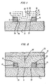
- reference numeral 11 denotes a substrate which may be, for example, silicon, epitaxial silicon, or silicon dioxide.
- Topographic features denoted by reference numerals 13 and 15 may be, for example, conductive runners.
- the conductive runners may be made from metal such as aluminum or tungsten, or from polysilicon or silicide or polycide.
- Each feature, 13 and 15, has a sidewall denoted by reference numerals 39 and 37, respectively, and a top surface denoted by reference numerals 35 and 33, respectively.
- Sidewalls 37 and 39 are generally perpendicular to substrate 11. Sidewalls 37 and 39, together with upper surface 31 of substrate 11 define a space 46 between features 13 and 15.
- Fig. 1 illustrates what happens when a conformal layer is deposited over features 13 and 15 and in the aforementioned space 46.
- the chemical vapor deposition processes used to deposit oxides of silicon are one-step processes
- phantom layers 17, 19, and 21 provide successive snapshot or "stop-action views" during successive stages of the deposition of a conformal layer.
- space 43 is associated with phantom layer 17
- space 41 is associated with phantom layer 19
- space 25 is associated with phantom layer 21.
- Examining phantom layers 17, 19, and 21, in sequence one sees that, as the deposition process proceeds, a layer of uniform thickness is deposited on the sidewalls 39 and 37 and along the surface 31 of substrate 11.
- the aspect ratio of spaces 43, 41 and, ultimately, 25 becomes progressively larger.
- the aspect ratio is defined as the height of the space divided by its width.
- the layers on the sides 39 and 37 are growing toward each other more rapidly than the layer contacting surface 31 of substrate 11 is growing upward. In other words, the space between features 13 and 15 fills or closes more rapidly from the sides than from the bottom.
- Fig. 1 illustrates a hitherto unrealized disadvantage of conformal layers.
- the conformal filling process creates a space with a dynamic (e.g. changing) aspect ratio. As the aspect ratio of spaces 43, 41 and 25 becomes progressively larger (and spaces 43, 41, and 25 become increasingly smaller), it becomes increasingly difficult to fill each space. The precise mechanism responsible for the formation of the low-density region has not been determined. If the deposition process is performed without plasma enhancement, the primary deposition mechanism is surface migration of the reactant species.
- FIG. 2 The final result of the filling process is shown in Fig. 2.
- reference numerals 23 denotes the completed conformal layer.
- Reference numerals 25′ denotes a low-density region or "soft oxide", which is formed by the closure of space 25 shown in Fig. 1. It will be noted, from an examination of Fig. 2, that after soft oxide region 25′ is formed, the dielectric is deposited relatively uniformly above imaginary reference line 27 (which demarcates the top of low-density region 25′).
- an etch-back procedure is used to reduce the thickness of dielectric 23.
- An anisotropic etch-back procedure uniformly reduces the thickness of layer 23 toward substrate 11.
- the anisotropic etching procedure (together with subsequent wet cleaning procedures) will preferentially attack soft oxide area 25′, creating a groove in dielectric 23.
- a wet cleaning procedure used to remove sodium residue after anisotropic etching exhibits great preference for the low-density region.
- the wet cleaning procedure uses either an 8:1 ratio of ethylene glycol and buffered HF if aluminum runners are exposed, or a 100:1 ratio of water and HF if no aluminum is exposed.
- Figs. 1 and 2 illustrate that the use of a conformal layer creates an apparently solid dielectric, which may exhibit an unexpected groove during subsequent etching.
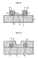
- Conformality is often described by various ratios. Referring to Fig. 3, the conformality of layer 10 may be conveniently described by the ratio s t , where t is the thickness of layer 18 above top surface 35 of feature 13, and s is the thickness of the same layer 10 measured outward from sidewall 39 of feature 13 at a point near the top of feature 13. Another measure of conformality is the ratio, b s , where b is the thickness of layer 10 measured at a point near the bottom sidewall 39.
- Dielectric layers deposited from the various organometallic precursors mentioned before exhibit varying degrees of conformality, as measured by the above-mentioned ratios.
- plasma-enhanced TEOS-based dielectrics have an s t ratio of roughly 0.5 to 0.6, while the same ratio for plasma-enhanced DADBS is roughly 0.7 to 0.8, and for TMCTS is roughly 0.5 to 0.6.
- the s t ratio be high, i.e., near 1.
- the s t ratio governs the minimum thickness of dielectric (measured, for example, upward from surface 35), which must be deposited to assure filling the space between features 13 and 15 (since the space, as noted before, fills from the sides).
- the ratio, b s is more important to the successful practice of this invention.
- the ratio, b s should be as close to 1 as possible. All of the aforementioned organometallics exhibit a satisfactory b s ratio (with typical values of roughly greater than, or equal to, 0.9 in plasma-enhanced deposition. If the b s ratio is much less than 1.0, the layer 10 assumes a re-entrant shape and, consequently, fabrication of fillets or spacers with the convex profile, which will aid in the practice if the invention becomes difficult.
- the low-density region such as that illustrated by reference numeral 25′ in Fig. 2, is not the same as a void.
- a void is the absence of any material.
- a low-density region is generally solid, although probably of non-stoichiometric composition.
- each organometallic precursor for silicon oxide has a fairly characteristic b s ratio.
- the initial aspect ratio of the space to be filled is important in determining whether a void is formed or a low-density region is formed. If the initial aspect ratio is high and the material's conformality (as measured by the b s ratio) is relatively low, there is a likelihood that voids will form as the space is filled. Fillets, or spacers, have been previously employed in an effort to eliminate such voids. However, if the aspect ratio is lower, or if the material's conformality (as measured by the b s ratio) is high, the likelihood of void formation is reduced, but the likelihood of low-density region formation increases. It has already been mentioned, in connection with Fig. 2, that after the low-density region has formed, further deposition of the dielectric proceeds to cover, and thus hide, the low-density region.
- the existence of the low-density region comes as a surprise to practitioners who subsequently etch away the outer portion of seemingly "solid" or voidless dielectrics.
- the etchant encounters the low-density region and preferentially attacks it.
- the low-density region is etched away significantly faster than the surrounding dielectric.
- a groove then appears where the low-density region had been.
- the groove appears in an area which heretofore had been believed solid, or of uniform density.
- the problem is further aggravated because of the anisotropic etching procedure used.
- the anisotropic process transfers the groove downward toward the conductors or topographic features which have been covered. The result is that a groove appears between the conductors or topographic features.
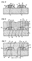
- Figs. 4-6 illustrate applicant's inventive process for eliminating the low-density area 25′.
- Figs. 4 and 5 illustrate the spacer-forming process, while Figs. 6 and 7 illustrate the subsequent filling of the space between features 13 and 15.
- the spacers are formed by first depositing a layer 51 over the tops 35 and 33 of features 13 and 15, respectively. It will be noted that layer 51 also fills in the space defined by sidewalls 37 and 39, together with upper surface 31 of substrate 11. Layer 51 should not be deposited so thickly that a low-density region, such as 25′ in Fig. 2, is formed.
- layer 51 may be made from a conformal material, such as one of the aforementioned organometallics.
- a non-conformal layer e.g., formed from silane
- the deposition process may be plasma enhanced so that the deposition temperature may be kept low enough to avoid damage to the aluminum. It is also possible to use silicon nitride to form the spacers.
- layer 51 After layer 51 has been deposited, it is etched-back by anisotropic etching procedures well known to those skilled in the art to produce spacers 57, 55, 59 and 60 illustrated in Fig. 5. (If layer 51 had been deposited as thick as illustrated in Fig. 2, it would not be possible to form spacers because the anisotropic etching process generally transfers the contour of the upper surface downward.) If desired, the etching procedure need not be carried out completely and upper surface 31 of substrate 11, together with tops 33 and 35 of features 15 and 13, respectively, may be covered with a thin layer of conformal layer 51.
- An exemplary process suitable for the anisotropic etching of layer 51 is by reactive ion etching with CHF3 and O2 at 60 sccm and 7 sccm, respectively, at 1400 watts power and 65 millitorr pressure, in an hexode reactor.
- Other methods will occur to those skilled in the art.
- the above etching process when used upon TEOS layers, produces spacers with cross-sections somewhat resembling quarter (i.e., 1/4) circles.
- the quarter circle spacers perform nicely in the practice of this invention, although both spacers with somewhat steeper or flatter profiles will also work. (If a non-conformal material is used to form the spacers, a steeper profile will obtain.)
- a conformal layer 79 is deposited over features 13 and 15.
- Phantom layers 71, 73, 75 and 77 show successive steps or "stop-action views" in the continuous deposition of conformal layer 79.
- Fig. 7 illustrates the structure of Fig. 5 after a standard etch-back procedure has been applied.
- the etch-back procedure thins conformal layer 79, yielding outer surface 81.
- the same anisotropic reactive ion etching procedure described above may be utilized, although other procedures known to those skilled in the art may be used.
- features 13 and 15 are aluminum first-level metal runners.
- the runners are approximately 5000 ⁇ high and have steep sides. In some instances, the distance between adjacent runners may be roughly one micron (denoted by dimension "d” in Fig. 7).
- the spacers have a base width of approximately 3000 ⁇ each (denoted by dimension "s” in Fig. 7).
- the spacers have been formed by depositing TEOS in a plasma-enhanced deposition chamber with an initial thickness of 6000 ⁇ and etching it back to 4000 ⁇ as well as permitting a thickness of approximately 2000 ⁇ to cover surfaces 31, 35 and 33. Next, a thermal plasma enhanced TEOS deposition is performed to an initial thickness of 25,0000 ⁇ . Finally, the second TEOS layer is etched back to a final thickness of 8000 ⁇ .
Landscapes
- Formation Of Insulating Films (AREA)
- Internal Circuitry In Semiconductor Integrated Circuit Devices (AREA)
Applications Claiming Priority (2)
| Application Number | Priority Date | Filing Date | Title |
|---|---|---|---|
| US37450489A | 1989-06-30 | 1989-06-30 | |
| US374504 | 1989-06-30 |
Publications (2)
| Publication Number | Publication Date |
|---|---|
| EP0405850A2 true EP0405850A2 (de) | 1991-01-02 |
| EP0405850A3 EP0405850A3 (de) | 1991-03-13 |
Family
ID=23477130
Family Applications (1)
| Application Number | Title | Priority Date | Filing Date |
|---|---|---|---|
| EP19900306835 Withdrawn EP0405850A3 (de) | 1989-06-30 | 1990-06-22 | Dielektrikum-Herstellungsverfahren und dadurch hergestellte Komponente |
Country Status (2)
| Country | Link |
|---|---|
| EP (1) | EP0405850A3 (de) |
| JP (1) | JPH0338828A (de) |
Cited By (5)
| Publication number | Priority date | Publication date | Assignee | Title |
|---|---|---|---|---|
| EP0528690A1 (de) * | 1991-08-21 | 1993-02-24 | STMicroelectronics, Inc. | Kontaktausrichtung für Festwertspeicher |
| EP0528691A1 (de) * | 1991-08-21 | 1993-02-24 | STMicroelectronics, Inc. | Kontaktausrichtung für integrierte Schaltkreise |
| US5286672A (en) * | 1991-06-28 | 1994-02-15 | Sgs-Thomson Microelectronics, Inc. | Method for forming field oxide regions |
| EP0599074A1 (de) * | 1992-11-20 | 1994-06-01 | Deutsche ITT Industries GmbH | Verfahren zur globalen Planarisierung von Oberflächen integrierter Halbleiterchaltungen |
| WO1997013272A1 (en) * | 1995-10-04 | 1997-04-10 | Advanced Micro Devices, Inc. | An efficient and economical method of planarization of multilevel metallization structures in integrated circuits using cmp |
Family Cites Families (2)
| Publication number | Priority date | Publication date | Assignee | Title |
|---|---|---|---|---|
| US4666737A (en) * | 1986-02-11 | 1987-05-19 | Harris Corporation | Via metallization using metal fillets |
| GB2220298A (en) * | 1988-06-29 | 1990-01-04 | Philips Nv | A method of manufacturing a semiconductor device |
-
1990
- 1990-06-22 EP EP19900306835 patent/EP0405850A3/de not_active Withdrawn
- 1990-06-26 JP JP2165876A patent/JPH0338828A/ja active Pending
Cited By (10)
| Publication number | Priority date | Publication date | Assignee | Title |
|---|---|---|---|---|
| US5286672A (en) * | 1991-06-28 | 1994-02-15 | Sgs-Thomson Microelectronics, Inc. | Method for forming field oxide regions |
| EP0528690A1 (de) * | 1991-08-21 | 1993-02-24 | STMicroelectronics, Inc. | Kontaktausrichtung für Festwertspeicher |
| EP0528691A1 (de) * | 1991-08-21 | 1993-02-24 | STMicroelectronics, Inc. | Kontaktausrichtung für integrierte Schaltkreise |
| US5231043A (en) * | 1991-08-21 | 1993-07-27 | Sgs-Thomson Microelectronics, Inc. | Contact alignment for integrated circuits |
| US5376571A (en) * | 1991-08-21 | 1994-12-27 | Sgs-Thomson Microelectronics, Inc. | Method of making contact alignment for nonvolatile memory devices |
| US5448091A (en) * | 1991-08-21 | 1995-09-05 | Sgs-Thomson Microelectronics, Inc. | Method of making contact alignment for nonvolatile memory devices |
| EP0599074A1 (de) * | 1992-11-20 | 1994-06-01 | Deutsche ITT Industries GmbH | Verfahren zur globalen Planarisierung von Oberflächen integrierter Halbleiterchaltungen |
| US5445998A (en) * | 1992-11-20 | 1995-08-29 | Deutsche Itt Industries Gmbh | Method for the global planarization of surfaces of semiconductor integrated circuits |
| WO1997013272A1 (en) * | 1995-10-04 | 1997-04-10 | Advanced Micro Devices, Inc. | An efficient and economical method of planarization of multilevel metallization structures in integrated circuits using cmp |
| US5840623A (en) * | 1995-10-04 | 1998-11-24 | Advanced Micro Devices, Inc. | Efficient and economical method of planarization of multilevel metallization structures in integrated circuits using CMP |
Also Published As
| Publication number | Publication date |
|---|---|
| EP0405850A3 (de) | 1991-03-13 |
| JPH0338828A (ja) | 1991-02-19 |
Similar Documents
| Publication | Publication Date | Title |
|---|---|---|
| US5447884A (en) | Shallow trench isolation with thin nitride liner | |
| EP0048175B1 (de) | Halbleiterbauelement und Verfahren zu dessen Herstellung | |
| US5841196A (en) | Fluted via formation for superior metal step coverage | |
| US4952524A (en) | Semiconductor device manufacture including trench formation | |
| US6743727B2 (en) | Method of etching high aspect ratio openings | |
| US4791073A (en) | Trench isolation method for semiconductor devices | |
| EP0084635A2 (de) | Verfahren zur Herstellung einer tiefen und breiten Grube gefüllt mit Dielektrikum in einer Oberfläche eines Halbleitersubstrats aus Silizium | |
| EP0871213A2 (de) | Verfahren zur Bildung von Kontaktbohrungen mit variablem Seitenwandprofil | |
| US4601781A (en) | Method for improving step coverage of dielectrics in VLSI circuits | |
| US5489553A (en) | HF vapor surface treatment for the 03 teos gap filling deposition | |
| US20050136686A1 (en) | Gap-fill method using high density plasma chemical vapor deposition process and method of manufacturing integrated circuit device | |
| US4708767A (en) | Method for providing a semiconductor device with planarized contacts | |
| JPH08250497A (ja) | 半導体装置の金属配線層の形成方法 | |
| US6809004B2 (en) | Method of forming a shallow trench isolation | |
| US20030224580A1 (en) | Novel deposition and sputter etch approach to extend the gap fill capability of HDP CVD process to less than or equal to 0.10 microns | |
| US6197660B1 (en) | Integration of CMP and wet or dry etching for STI | |
| US5567650A (en) | Method of forming tapered plug-filled via in electrical interconnection | |
| EP0405850A2 (de) | Dielektrikum-Herstellungsverfahren und dadurch hergestellte Komponente | |
| EP0257948A2 (de) | Durchgangsleitung für CMOS-Anordnungen | |
| US5888901A (en) | Multilevel interconnection and method for making | |
| EP0878836B1 (de) | Planarisierung von einem Halbleitersubstrat | |
| US6849493B2 (en) | Methods of forming polished material and methods of forming isolation regions | |
| US4594769A (en) | Method of forming insulator of selectively varying thickness on patterned conductive layer | |
| US6091150A (en) | Integrated circuitry comprising electrically insulative material over interconnect line tops, sidewalls and bottoms | |
| CN1490866A (zh) | 浅沟道隔离区形成方法 |
Legal Events
| Date | Code | Title | Description |
|---|---|---|---|
| PUAI | Public reference made under article 153(3) epc to a published international application that has entered the european phase |
Free format text: ORIGINAL CODE: 0009012 |
|
| AK | Designated contracting states |
Kind code of ref document: A2 Designated state(s): DE ES FR GB IT |
|
| PUAL | Search report despatched |
Free format text: ORIGINAL CODE: 0009013 |
|
| RHK1 | Main classification (correction) |
Ipc: H01L 21/90 |
|
| AK | Designated contracting states |
Kind code of ref document: A3 Designated state(s): DE ES FR GB IT |
|
| 17P | Request for examination filed |
Effective date: 19910905 |
|
| STAA | Information on the status of an ep patent application or granted ep patent |
Free format text: STATUS: THE APPLICATION HAS BEEN WITHDRAWN |
|
| 18W | Application withdrawn |
Withdrawal date: 19910919 |