EP0405828B1 - Solder assembly of components - Google Patents
Solder assembly of components Download PDFInfo
- Publication number
- EP0405828B1 EP0405828B1 EP90306739A EP90306739A EP0405828B1 EP 0405828 B1 EP0405828 B1 EP 0405828B1 EP 90306739 A EP90306739 A EP 90306739A EP 90306739 A EP90306739 A EP 90306739A EP 0405828 B1 EP0405828 B1 EP 0405828B1
- Authority
- EP
- European Patent Office
- Prior art keywords
- component
- solder
- pad areas
- pad
- holes
- Prior art date
- Legal status (The legal status is an assumption and is not a legal conclusion. Google has not performed a legal analysis and makes no representation as to the accuracy of the status listed.)
- Expired - Lifetime
Links
Images



Classifications
-
- H—ELECTRICITY
- H05—ELECTRIC TECHNIQUES NOT OTHERWISE PROVIDED FOR
- H05K—PRINTED CIRCUITS; CASINGS OR CONSTRUCTIONAL DETAILS OF ELECTRIC APPARATUS; MANUFACTURE OF ASSEMBLAGES OF ELECTRICAL COMPONENTS
- H05K3/00—Apparatus or processes for manufacturing printed circuits
- H05K3/30—Assembling printed circuits with electric components, e.g. with resistors
- H05K3/32—Assembling printed circuits with electric components, e.g. with resistors electrically connecting electric components or wires to printed circuits
- H05K3/34—Assembling printed circuits with electric components, e.g. with resistors electrically connecting electric components or wires to printed circuits by soldering
- H05K3/3465—Application of solder
- H05K3/3485—Application of solder paste, slurry or powder
-
- H—ELECTRICITY
- H05—ELECTRIC TECHNIQUES NOT OTHERWISE PROVIDED FOR
- H05K—PRINTED CIRCUITS; CASINGS OR CONSTRUCTIONAL DETAILS OF ELECTRIC APPARATUS; MANUFACTURE OF ASSEMBLAGES OF ELECTRICAL COMPONENTS
- H05K3/00—Apparatus or processes for manufacturing printed circuits
- H05K3/36—Assembling printed circuits with other printed circuits
- H05K3/361—Assembling flexible printed circuits with other printed circuits
- H05K3/363—Assembling flexible printed circuits with other printed circuits by soldering
-
- H—ELECTRICITY
- H05—ELECTRIC TECHNIQUES NOT OTHERWISE PROVIDED FOR
- H05K—PRINTED CIRCUITS; CASINGS OR CONSTRUCTIONAL DETAILS OF ELECTRIC APPARATUS; MANUFACTURE OF ASSEMBLAGES OF ELECTRICAL COMPONENTS
- H05K1/00—Printed circuits
- H05K1/02—Details
- H05K1/0266—Marks, test patterns or identification means
- H05K1/0269—Marks, test patterns or identification means for visual or optical inspection
-
- H—ELECTRICITY
- H05—ELECTRIC TECHNIQUES NOT OTHERWISE PROVIDED FOR
- H05K—PRINTED CIRCUITS; CASINGS OR CONSTRUCTIONAL DETAILS OF ELECTRIC APPARATUS; MANUFACTURE OF ASSEMBLAGES OF ELECTRICAL COMPONENTS
- H05K2201/00—Indexing scheme relating to printed circuits covered by H05K1/00
- H05K2201/10—Details of components or other objects attached to or integrated in a printed circuit board
- H05K2201/10613—Details of electrical connections of non-printed components, e.g. special leads
- H05K2201/10621—Components characterised by their electrical contacts
- H05K2201/10666—Plated through-hole for surface mounting on PCB
-
- H—ELECTRICITY
- H05—ELECTRIC TECHNIQUES NOT OTHERWISE PROVIDED FOR
- H05K—PRINTED CIRCUITS; CASINGS OR CONSTRUCTIONAL DETAILS OF ELECTRIC APPARATUS; MANUFACTURE OF ASSEMBLAGES OF ELECTRICAL COMPONENTS
- H05K2203/00—Indexing scheme relating to apparatus or processes for manufacturing printed circuits covered by H05K3/00
- H05K2203/01—Tools for processing; Objects used during processing
- H05K2203/0104—Tools for processing; Objects used during processing for patterning or coating
- H05K2203/0113—Female die used for patterning or transferring, e.g. temporary substrate having recessed pattern
-
- H—ELECTRICITY
- H05—ELECTRIC TECHNIQUES NOT OTHERWISE PROVIDED FOR
- H05K—PRINTED CIRCUITS; CASINGS OR CONSTRUCTIONAL DETAILS OF ELECTRIC APPARATUS; MANUFACTURE OF ASSEMBLAGES OF ELECTRICAL COMPONENTS
- H05K2203/00—Indexing scheme relating to apparatus or processes for manufacturing printed circuits covered by H05K3/00
- H05K2203/01—Tools for processing; Objects used during processing
- H05K2203/0195—Tool for a process not provided for in H05K3/00, e.g. tool for handling objects using suction, for deforming objects, for applying local pressure
-
- H—ELECTRICITY
- H05—ELECTRIC TECHNIQUES NOT OTHERWISE PROVIDED FOR
- H05K—PRINTED CIRCUITS; CASINGS OR CONSTRUCTIONAL DETAILS OF ELECTRIC APPARATUS; MANUFACTURE OF ASSEMBLAGES OF ELECTRICAL COMPONENTS
- H05K2203/00—Indexing scheme relating to apparatus or processes for manufacturing printed circuits covered by H05K3/00
- H05K2203/03—Metal processing
- H05K2203/0338—Transferring metal or conductive material other than a circuit pattern, e.g. bump, solder, printed component
-
- H—ELECTRICITY
- H05—ELECTRIC TECHNIQUES NOT OTHERWISE PROVIDED FOR
- H05K—PRINTED CIRCUITS; CASINGS OR CONSTRUCTIONAL DETAILS OF ELECTRIC APPARATUS; MANUFACTURE OF ASSEMBLAGES OF ELECTRICAL COMPONENTS
- H05K2203/00—Indexing scheme relating to apparatus or processes for manufacturing printed circuits covered by H05K3/00
- H05K2203/04—Soldering or other types of metallurgic bonding
- H05K2203/043—Reflowing of solder coated conductors, not during connection of components, e.g. reflowing solder paste
-
- H—ELECTRICITY
- H05—ELECTRIC TECHNIQUES NOT OTHERWISE PROVIDED FOR
- H05K—PRINTED CIRCUITS; CASINGS OR CONSTRUCTIONAL DETAILS OF ELECTRIC APPARATUS; MANUFACTURE OF ASSEMBLAGES OF ELECTRICAL COMPONENTS
- H05K3/00—Apparatus or processes for manufacturing printed circuits
- H05K3/22—Secondary treatment of printed circuits
- H05K3/28—Applying non-metallic protective coatings
- H05K3/281—Applying non-metallic protective coatings by means of a preformed insulating foil
-
- H—ELECTRICITY
- H05—ELECTRIC TECHNIQUES NOT OTHERWISE PROVIDED FOR
- H05K—PRINTED CIRCUITS; CASINGS OR CONSTRUCTIONAL DETAILS OF ELECTRIC APPARATUS; MANUFACTURE OF ASSEMBLAGES OF ELECTRICAL COMPONENTS
- H05K3/00—Apparatus or processes for manufacturing printed circuits
- H05K3/30—Assembling printed circuits with electric components, e.g. with resistors
- H05K3/32—Assembling printed circuits with electric components, e.g. with resistors electrically connecting electric components or wires to printed circuits
- H05K3/34—Assembling printed circuits with electric components, e.g. with resistors electrically connecting electric components or wires to printed circuits by soldering
- H05K3/3452—Solder masks
Definitions
- soldering of components is often a critical operation in the fabrication of circuits and devices since failure to form an effective solder joint can result in costly yield and reliability problems. These problems are especially prevalent when an area array of solder joints is needed.
- a flexible printed circuit may be used to electrically connect a contact element to a rigid printed circuit board.
- the flexible circuit might preferably terminate in an area array which must be electrically coupled to corresponding terminations on the printed circuit board.
- One technique for attachment involves the use of conductive pins inserted in holes formed in the corresponding terminations in the flexible circuit and circuit board. (See, for example, U.S. Patent 4,806,107.) It would be more desirable to solder the flexible circuit directly to the circuit board since that would provide for improved electrical performance of the circuits and eliminate the need for extra piece parts.
- soldering of components Another concern in soldering of components is to provide just the right amount of solder to the pad arrays for forming an effective solder joint. Inadequate amount of solder can lead to problems in forming reliable solder joints with high yield, and excessive solder can result in formation of solder bridges between adjacent conducting elements and hence the need for repair.
- Plating often does not deposit an adequate solder volume dependably. Solder dipping is a possible approach to providing an enhanced solder coating on components, but the lack of control of solder volume leads to lack of control over the assembly process which produces assembly yield problems.
- Another approach, which is often used for surface mounted components is to deposit the solder in the form of a paste through apertures in a stencil.
- the board is typically made of an epoxy-glass material and the conductive pads are typically copper.
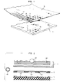
- the printed circuit board also usually includes a solder mask material, which is shown as 16 in FIGS. 2-10, but is not shown in FIG. 1 for the sake of clarity. This solder mask material covers essentially the entire printed circuit board except for the pads which will be soldered.
- the flexible circuit, 10 includes a cover layer which is shown as layers 17 and 18 in FIG. 10, on both surfaces of the circuit, but which is also not shown in FIG. 1 for clarity.
- the solder mask and cover layer act to provide control of the solder wettable areas of the two components.
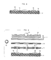
- the shuttle, 20 is aligned with the printed circuit board, 14, as illustrated in FIG. 2 so that each cavity is above its corresponding pad. Alignment can be effectuated with standard tooling pins (not shown). The solder will remain in the cavities due to its tacky consistency at room temperature.
- the aligned shuttle and printed circuit board are positioned under a soldering head which comprises a hot ram, 22, and a spring-loaded hold-down element, 23.
- the hot ram includes a heater element, 24, to produce the desired temperature at the soldering surface.
- the hot ram is typically formed from a block of copper plated with nickel and the heater element is a conventional electrically resistive element.
- FIG. 6 illustrates the placement of the flexible circuit, 10, in the apparatus of FIG. 2 for soldering to the printed circuit board, 14.
- the flexible circuit is aligned with the board, again, by the use of standard tooling pins (not shown), so that the holes, such as 13, are positioned above and aligned with corresponding pads, such as 15, on the board.
- a shuttle element, 20, can be used for this portion of the operation as a cover plate, with the cavities, 21, empty and aligned with their corresponding holes, 13, and pads, 15.
Landscapes
- Engineering & Computer Science (AREA)
- Manufacturing & Machinery (AREA)
- Microelectronics & Electronic Packaging (AREA)
- Electric Connection Of Electric Components To Printed Circuits (AREA)
- Manufacturing Of Electrical Connectors (AREA)
- Combinations Of Printed Boards (AREA)
Description
Claims (7)
- A method for electrically attaching a first component to a second component comprising the steps of:characterized in the steps of:providing metalized holes (13) in pad areas (12) of the first component (10) to be attached to corresponding pad areas (15) of the second component (14); andforming the pad areas of the first and second component in an urea array;depositing solder in a shuttle element (20) including cavities (21) which match with the said corresponding areas (15) of the second component so that each cavity includes predetermined amount of solder;aligning the shuttle (20) with the second component so that each of said cavities (21) is above and matches with each of said corresponding pad areas (15) of the second component and depositing said predetermined amount of solder (30) on the pad areas of the second component;bringing the first component into contact with the solder on the second component so that the holes are aligned with the corresponding pad areas (15); andheating the components to melt the solder and to cause the solder to form individual fillets (31) extending through the metalized holes so that each fillet is formed by the solder extending through the hole so as to cover a portion of the pad area (12) of the first component (10) including the hole but not including the edges of the pad area (12) of the first component and is observable from above the first component.
- The method according to claim 1, wherein one component is flexible and the other is rigid.
- The method according to claim 2 wherein one component is a flexible circuit and the other component is a printed circuit board.
- The method according to claim 1, wherein the predetermined amount of solder is such that the solder makes contact with the pad areas of the first component before any other portions of the two components make contact.
- The method according to claim I. wherein a cover plate (20) is held over the first and second components while the solder is melted to form the fillet, the cover plate including cavities (21) aligned with the holes in the first component, the cavities having a sufficient depth to permit the formation of a free surface fillet above the holes.
- A device comprising:CHARACTERIZED IN THATa first component being a flexible circuit (10) with pad areas (12) and a second component being a printed circuit board (14) with pad areas (15) surrounded by a mask material (16) on a facing surface, and the pad areas (12) of the first component include conductive portions with holes (13) formed therethrough and surrounded by a cover layer (17) on a facing surface, the mask material and cover layer providing control of the pad areas (12,15) of the two components which are wettable by solder;the pad areas (12,15) are arranged in an area array ;individual solder fillets (31) are formed between the pad areas (12) of the first component and the pad areas (15) of the second component on said facing surfaces and extend through said holes (13) to associated pad areas (12) on the surface of said first component opposite to its facing surface so that each fillet on each associated pad areas (12) coveres a portion of the associated pad area (12) including the hole but not including the edges of the associated pad area (12) and is observable from above the first component.
- The device according to claim 6, wherein the walls of the holes (13) are plated with metal which extends from the pad areas (12) of the facing surface to the associated pad areas (12) of the opposite surface of said first component.
Applications Claiming Priority (2)
| Application Number | Priority Date | Filing Date | Title |
|---|---|---|---|
| US372400 | 1989-06-27 | ||
| US07/372,400 US5014162A (en) | 1989-06-27 | 1989-06-27 | Solder assembly of components |
Publications (2)
| Publication Number | Publication Date |
|---|---|
| EP0405828A1 EP0405828A1 (en) | 1991-01-02 |
| EP0405828B1 true EP0405828B1 (en) | 1998-09-23 |
Family
ID=23467948
Family Applications (1)
| Application Number | Title | Priority Date | Filing Date |
|---|---|---|---|
| EP90306739A Expired - Lifetime EP0405828B1 (en) | 1989-06-27 | 1990-06-20 | Solder assembly of components |
Country Status (5)
| Country | Link |
|---|---|
| US (1) | US5014162A (en) |
| EP (1) | EP0405828B1 (en) |
| JP (1) | JPH0714106B2 (en) |
| CA (1) | CA2011000C (en) |
| DE (1) | DE69032671T2 (en) |
Cited By (1)
| Publication number | Priority date | Publication date | Assignee | Title |
|---|---|---|---|---|
| CN100454669C (en) * | 2007-07-26 | 2009-01-21 | 友达光电股份有限公司 | Electrical connection device, electronic device comprising same and electronic product |
Families Citing this family (34)
| Publication number | Priority date | Publication date | Assignee | Title |
|---|---|---|---|---|
| GB9113455D0 (en) * | 1991-06-21 | 1991-08-07 | Gore W L & Ass Uk | Improvements in security enclosures |
| GB9115972D0 (en) * | 1991-07-24 | 1991-09-11 | Gore W L & Ass Uk | Improvements in security enclosures |
| JPH0529178U (en) * | 1991-09-24 | 1993-04-16 | 日本電気株式会社 | Flexible printed circuit board |
| DE4132995A1 (en) * | 1991-10-04 | 1993-04-08 | Bodenseewerk Geraetetech | METHOD FOR PRODUCING ELECTRICALLY CONDUCTIVE CONNECTIONS ON PCB |
| US5211328A (en) * | 1992-05-22 | 1993-05-18 | International Business Machines | Method of applying solder |
| US5416278A (en) * | 1993-03-01 | 1995-05-16 | Motorola, Inc. | Feedthrough via connection |
| US5401913A (en) * | 1993-06-08 | 1995-03-28 | Minnesota Mining And Manufacturing Company | Electrical interconnections between adjacent circuit board layers of a multi-layer circuit board |
| CA2156795C (en) * | 1994-08-31 | 1999-08-17 | Yuzo Shimada | An electronic device assembly and a manufacturing method of the same |
| US5686697A (en) | 1995-01-06 | 1997-11-11 | Metatech Corporation | Electrical circuit suspension system |
| US6293456B1 (en) | 1997-05-27 | 2001-09-25 | Spheretek, Llc | Methods for forming solder balls on substrates |
| US7819301B2 (en) * | 1997-05-27 | 2010-10-26 | Wstp, Llc | Bumping electronic components using transfer substrates |
| US7842599B2 (en) * | 1997-05-27 | 2010-11-30 | Wstp, Llc | Bumping electronic components using transfer substrates |
| US7654432B2 (en) | 1997-05-27 | 2010-02-02 | Wstp, Llc | Forming solder balls on substrates |
| US7288471B2 (en) * | 1997-05-27 | 2007-10-30 | Mackay John | Bumping electronic components using transfer substrates |
| US5988487A (en) * | 1997-05-27 | 1999-11-23 | Fujitsu Limited | Captured-cell solder printing and reflow methods |
| US6609652B2 (en) | 1997-05-27 | 2003-08-26 | Spheretek, Llc | Ball bumping substrates, particuarly wafers |
| US7007833B2 (en) | 1997-05-27 | 2006-03-07 | Mackay John | Forming solder balls on substrates |
| WO1999048642A1 (en) * | 1998-03-23 | 1999-09-30 | Spheretek, Llc | Methods and apparatuses for forming solder balls on substrates |
| US6583364B1 (en) * | 1999-08-26 | 2003-06-24 | Sony Chemicals Corp. | Ultrasonic manufacturing apparatuses, multilayer flexible wiring boards and processes for manufacturing multilayer flexible wiring boards |
| JP2001210919A (en) * | 1999-11-17 | 2001-08-03 | Sharp Corp | Flexible wiring board and electronic device using the same |
| DE10126655A1 (en) | 2001-06-01 | 2002-12-05 | Endress & Hauser Gmbh & Co Kg | Circuit board for electronic equipment, has electronic component on first surface with first and second contact surfaces connected by solder or adhesive to first and second contact points with access to track |
| DE10301352B3 (en) * | 2003-01-16 | 2004-07-15 | Saint-Gobain Sekurit Deutschland Gmbh & Co. Kg | Solder terminal element for connecting electrical conductor with conductor structure applied to substrate e.g. automobile windscreen |
| DE102004038401B4 (en) * | 2003-10-14 | 2017-07-06 | Conti Temic Microelectronic Gmbh | Method for connecting a flexible flat conductor to a printed circuit board |
| JP4416616B2 (en) * | 2004-09-29 | 2010-02-17 | 株式会社リコー | Electronic component mounting body and electronic equipment |
| JP2007250609A (en) * | 2006-03-14 | 2007-09-27 | Funai Electric Co Ltd | Wiring board |
| DE102006058731A1 (en) * | 2006-12-13 | 2008-07-17 | Robert Bosch Gmbh | PCB connection |
| FR2960378B1 (en) * | 2010-05-21 | 2014-11-21 | Valeo Vision | ASSEMBLY OF AT LEAST TWO ELECTRIC CARDS |
| JP5380720B2 (en) * | 2010-08-31 | 2014-01-08 | 株式会社山石屋洋琴工房 | Touch feeling adjustment plate and piano adjustment method |
| JP2014192476A (en) * | 2013-03-28 | 2014-10-06 | Fujitsu Ltd | Printed circuit board solder packaging method and solder packaging structure |
| KR101938105B1 (en) * | 2018-01-25 | 2019-01-14 | 주식회사 기가레인 | Flexible circuit board with improved bonding position accuracy |
| CN110505750B (en) * | 2019-08-28 | 2020-10-16 | 生益电子股份有限公司 | PCB detection method and PCB |
| CN113923890B (en) * | 2021-09-16 | 2022-09-27 | 景旺电子科技(龙川)有限公司 | Circuit board mounting method and circuit board |
| CN115066092B (en) * | 2021-10-09 | 2023-03-24 | 荣耀终端有限公司 | Circuit board assembly, manufacturing method and electronic equipment |
| KR102943942B1 (en) * | 2023-11-27 | 2026-03-27 | 주식회사 웨이브컴퍼니 | Bonding structure in electrically conductive pattern of fabric |
Family Cites Families (10)
| Publication number | Priority date | Publication date | Assignee | Title |
|---|---|---|---|---|
| DE7110700U (en) * | 1970-03-27 | 1976-05-06 | Owens-Illinois Inc., Toledo, Ohio (V.St.A.) | Gas discharge field |
| US3676746A (en) * | 1970-12-23 | 1972-07-11 | Honeywell Inf Systems | Compatible modular circuit board connector |
| JPS5016863A (en) * | 1973-06-20 | 1975-02-21 | ||
| DE2451343C3 (en) * | 1973-10-26 | 1978-10-05 | Matsushita Electric Industrial Co., Ltd., Kadoma, Osaka (Japan) | Printed circuit |
| US4064357A (en) * | 1975-12-02 | 1977-12-20 | Teledyne Electro-Mechanisms | Interconnected printed circuits and method of connecting them |
| DE2657313B2 (en) * | 1976-12-17 | 1978-10-12 | Siemens Ag, 1000 Berlin Und 8000 Muenchen | Method for connecting electrical components to the conductor tracks of a printed circuit board or carrier board |
| JPS57121297A (en) * | 1981-01-20 | 1982-07-28 | Sharp Kk | Method of producing composite printed board |
| US4437141A (en) * | 1981-09-14 | 1984-03-13 | Texas Instruments Incorporated | High terminal count integrated circuit device package |
| JPS6211800A (en) * | 1985-07-10 | 1987-01-20 | 伊藤 進 | Preparation for controlling precipitation of wax |
| US4806107A (en) * | 1987-10-16 | 1989-02-21 | American Telephone And Telegraph Company, At&T Bell Laboratories | High frequency connector |
-
1989
- 1989-06-27 US US07/372,400 patent/US5014162A/en not_active Expired - Fee Related
-
1990
- 1990-02-27 CA CA002011000A patent/CA2011000C/en not_active Expired - Fee Related
- 1990-06-05 JP JP2145572A patent/JPH0714106B2/en not_active Expired - Fee Related
- 1990-06-20 EP EP90306739A patent/EP0405828B1/en not_active Expired - Lifetime
- 1990-06-20 DE DE69032671T patent/DE69032671T2/en not_active Expired - Fee Related
Non-Patent Citations (3)
| Title |
|---|
| ELECTRONICS INTERNATIONAL, vol. 53, no. 23, October 1980, pages 290, 292, New York, US; New Products 'Tape delivers solder evenly' * |
| IBM TECHNICAL DISCLOSURE BULLETIN, vol. 25, no. 7A, December 1982, page 3177, New Jersey, US; N.G.AAKALU et al.:'Protective shield/Solder Dam for Substrates' * |
| IBM TECHNICAL DISCLOSURE BULLETIN, vol. 29, no. 4, September 1986, pages 1612, 1613, Armonk, NJ, US; 'Improved Lead Structure for Surface Mount Components' * |
Cited By (1)
| Publication number | Priority date | Publication date | Assignee | Title |
|---|---|---|---|---|
| CN100454669C (en) * | 2007-07-26 | 2009-01-21 | 友达光电股份有限公司 | Electrical connection device, electronic device comprising same and electronic product |
Also Published As
| Publication number | Publication date |
|---|---|
| CA2011000A1 (en) | 1990-12-27 |
| EP0405828A1 (en) | 1991-01-02 |
| JPH0335590A (en) | 1991-02-15 |
| CA2011000C (en) | 1997-12-09 |
| DE69032671D1 (en) | 1998-10-29 |
| DE69032671T2 (en) | 1999-04-15 |
| JPH0714106B2 (en) | 1995-02-15 |
| US5014162A (en) | 1991-05-07 |
Similar Documents
| Publication | Publication Date | Title |
|---|---|---|
| US5014162A (en) | Solder assembly of components | |
| US5048747A (en) | Solder assembly of components | |
| US5241134A (en) | Terminals of surface mount components | |
| US5129573A (en) | Method for attaching through-hole devices to a circuit board using solder paste | |
| US5217597A (en) | Solder bump transfer method | |
| US5172852A (en) | Soldering method | |
| KR910007103B1 (en) | Forming and Bonding Leads to Wireless Components | |
| KR100188625B1 (en) | Fine pitch solder deposits on printed circuit board process and product | |
| US4934582A (en) | Method and apparatus for removing solder mounted electronic components | |
| JP2004207232A (en) | Solder storage transferring device and step | |
| US4403410A (en) | Manufacture of printed circuit boards | |
| US4928387A (en) | Temporary soldering aid for manufacture of printed wiring assemblies | |
| JP2844778B2 (en) | How to solder two types of parts to a single-sided printed circuit board | |
| EP0784914B1 (en) | Method of manufacturing a printed circuit board | |
| US20030027415A1 (en) | Ball grid assembly with solder columns | |
| US5261989A (en) | Straddle mounting an electrical conductor to a printed circuit board | |
| CA1131746A (en) | Circuit board with mounted components and method for manufacture | |
| JP2002057453A (en) | Semiconductor device repair method | |
| JP3240687B2 (en) | Electronic component mounting method | |
| US5271549A (en) | Multiple-lead element soldering method using sheet solder | |
| JPS6364079B2 (en) | ||
| JP2699000B2 (en) | Electrode connection method for multilayer printed circuit board | |
| JPH07246492A (en) | Method for forming solder bump of electronic component and connecting solder | |
| JPH0718475U (en) | Printed wiring board | |
| JP3455053B2 (en) | Wiring board with connector and method of manufacturing the same |
Legal Events
| Date | Code | Title | Description |
|---|---|---|---|
| PUAI | Public reference made under article 153(3) epc to a published international application that has entered the european phase |
Free format text: ORIGINAL CODE: 0009012 |
|
| AK | Designated contracting states |
Kind code of ref document: A1 Designated state(s): DE FR GB IT NL |
|
| 17P | Request for examination filed |
Effective date: 19910619 |
|
| 17Q | First examination report despatched |
Effective date: 19931005 |
|
| RAP3 | Party data changed (applicant data changed or rights of an application transferred) |
Owner name: AT&T CORP. |
|
| GRAG | Despatch of communication of intention to grant |
Free format text: ORIGINAL CODE: EPIDOS AGRA |
|
| GRAG | Despatch of communication of intention to grant |
Free format text: ORIGINAL CODE: EPIDOS AGRA |
|
| GRAG | Despatch of communication of intention to grant |
Free format text: ORIGINAL CODE: EPIDOS AGRA |
|
| GRAH | Despatch of communication of intention to grant a patent |
Free format text: ORIGINAL CODE: EPIDOS IGRA |
|
| GRAH | Despatch of communication of intention to grant a patent |
Free format text: ORIGINAL CODE: EPIDOS IGRA |
|
| GRAA | (expected) grant |
Free format text: ORIGINAL CODE: 0009210 |
|
| AK | Designated contracting states |
Kind code of ref document: B1 Designated state(s): DE FR GB IT NL |
|
| REF | Corresponds to: |
Ref document number: 69032671 Country of ref document: DE Date of ref document: 19981029 |
|
| ET | Fr: translation filed | ||
| PLBE | No opposition filed within time limit |
Free format text: ORIGINAL CODE: 0009261 |
|
| STAA | Information on the status of an ep patent application or granted ep patent |
Free format text: STATUS: NO OPPOSITION FILED WITHIN TIME LIMIT |
|
| 26N | No opposition filed | ||
| REG | Reference to a national code |
Ref country code: GB Ref legal event code: IF02 |
|
| PGFP | Annual fee paid to national office [announced via postgrant information from national office to epo] |
Ref country code: FR Payment date: 20030518 Year of fee payment: 14 |
|
| PGFP | Annual fee paid to national office [announced via postgrant information from national office to epo] |
Ref country code: GB Payment date: 20030519 Year of fee payment: 14 |
|
| PGFP | Annual fee paid to national office [announced via postgrant information from national office to epo] |
Ref country code: NL Payment date: 20030605 Year of fee payment: 14 Ref country code: DE Payment date: 20030605 Year of fee payment: 14 |
|
| PG25 | Lapsed in a contracting state [announced via postgrant information from national office to epo] |
Ref country code: GB Free format text: LAPSE BECAUSE OF NON-PAYMENT OF DUE FEES Effective date: 20040620 |
|
| PG25 | Lapsed in a contracting state [announced via postgrant information from national office to epo] |
Ref country code: NL Free format text: LAPSE BECAUSE OF NON-PAYMENT OF DUE FEES Effective date: 20050101 Ref country code: DE Free format text: LAPSE BECAUSE OF NON-PAYMENT OF DUE FEES Effective date: 20050101 |
|
| GBPC | Gb: european patent ceased through non-payment of renewal fee |
Effective date: 20040620 |
|
| PG25 | Lapsed in a contracting state [announced via postgrant information from national office to epo] |
Ref country code: FR Free format text: LAPSE BECAUSE OF NON-PAYMENT OF DUE FEES Effective date: 20050228 |
|
| NLV4 | Nl: lapsed or anulled due to non-payment of the annual fee |
Effective date: 20050101 |
|
| REG | Reference to a national code |
Ref country code: FR Ref legal event code: ST |
|
| PG25 | Lapsed in a contracting state [announced via postgrant information from national office to epo] |
Ref country code: IT Free format text: LAPSE BECAUSE OF NON-PAYMENT OF DUE FEES Effective date: 20050620 |