EP0404560B1 - Multiprozessorsystem und Verfahren - Google Patents
Multiprozessorsystem und Verfahren Download PDFInfo
- Publication number
- EP0404560B1 EP0404560B1 EP90306777A EP90306777A EP0404560B1 EP 0404560 B1 EP0404560 B1 EP 0404560B1 EP 90306777 A EP90306777 A EP 90306777A EP 90306777 A EP90306777 A EP 90306777A EP 0404560 B1 EP0404560 B1 EP 0404560B1
- Authority
- EP
- European Patent Office
- Prior art keywords
- memory
- data item
- access
- subpage
- processors
- Prior art date
- Legal status (The legal status is an assumption and is not a legal conclusion. Google has not performed a legal analysis and makes no representation as to the accuracy of the status listed.)
- Expired - Lifetime
Links
Images

Classifications
-
- G—PHYSICS
- G06—COMPUTING OR CALCULATING; COUNTING
- G06F—ELECTRIC DIGITAL DATA PROCESSING
- G06F9/00—Arrangements for program control, e.g. control units
- G06F9/06—Arrangements for program control, e.g. control units using stored programs, i.e. using an internal store of processing equipment to receive or retain programs
- G06F9/30—Arrangements for executing machine instructions, e.g. instruction decode
- G06F9/38—Concurrent instruction execution, e.g. pipeline or look ahead
- G06F9/3861—Recovery, e.g. branch miss-prediction, exception handling
- G06F9/3865—Recovery, e.g. branch miss-prediction, exception handling using deferred exception handling, e.g. exception flags
-
- G—PHYSICS
- G06—COMPUTING OR CALCULATING; COUNTING
- G06F—ELECTRIC DIGITAL DATA PROCESSING
- G06F11/00—Error detection; Error correction; Monitoring
- G06F11/004—Error avoidance
-
- G—PHYSICS
- G06—COMPUTING OR CALCULATING; COUNTING
- G06F—ELECTRIC DIGITAL DATA PROCESSING
- G06F15/00—Digital computers in general; Data processing equipment in general
- G06F15/16—Combinations of two or more digital computers each having at least an arithmetic unit, a program unit and a register, e.g. for a simultaneous processing of several programs
- G06F15/163—Interprocessor communication
- G06F15/173—Interprocessor communication using an interconnection network, e.g. matrix, shuffle, pyramid, star, snowflake
- G06F15/17337—Direct connection machines, e.g. completely connected computers, point to point communication networks
Definitions
- This invention relates to digital data processing systems and, more particularly, to multiprocessing systems with distributed hierarchical memory architectures.
- the art provides a number of configurations for coupling the processing units of multiprocessing systems.
- processing units that shared data stored in system memory banks were coupled to those banks via high-bandwidth shared buses or switching networks.
- bottlenecks were likely to develop as multiple processing units simultaneously sought access to the shared data.
- a hierarchical approach is disclosed by Wilson Jr. et al, United Kingdom Patent Application No. 2,178,205, wherein a multiprocessing system is said to include distributed cache memory elements coupled with one another over a first bus.
- a second, higher level cache memory attached to the first bus retains copies of every memory location in the caches below it. Residing over the second level cache is a third, still higher level cache and the main system memory. Both the third level cache and the system main memory, in turn, retain copies of each memory location of the caches below them.
- Processors in the system are understood to transmit modified copies of data from their own dedicated caches to the associated higher level caches, as well as to the system main memory, while concurrently signalling other caches to invalidate their own copies of the newly-modified data.
- a further object is to provide a multiprocessing system with unlimited scalability.
- Another object of the invention is to provide a physically distributed memory multiprocessing system which requires little or no software overhead to maintain data coherency, as well as one with increased bus bandwidth and improved synchronization.
- a digital data processing system comprising memory means configured to store at least one data item; at least first and second processors, each configured to generate an access request for requesting access to the at least one data item stored in said memory means; and memory management means configured to receive access requests from said first and second processors, said memory management means being further configured: in a first mode, in response to an access request generated by any of said processors, to signal to the respective processor that generated the access request that the at least one data item is stored in said memory means; and in a second mode, in response to an access request generated by one of said processors, to signal the one of any processors that the at least one data item is stored in said memory means, and in response to an access request generated by another of said processors not to signal the other of said processors that the at least one data item is stored in said memory means.
- a method of operating a multiprocessor digital data processing system of the type having at least first and second processors, memory management means and memory means for storing at least one data item comprising the steps of: generating, within any of said processors, an access request requesting access to said at least one data item; and said memory management means selectively operating: in a first mode in response to an access request generated by any of said first processors, to signal the respective processor that generated the access request that the at least one data item is stored in said memory means, or in a second mode, in response to an access request generated by one of said processors, to signal the one of said processors that the at least one data item is stored in said memory means, and, in response to an access request generated by an other of said processors, not to signal the other of said processors that the at least one data item is stored in said memory means.
- the memory management element permits, inter alia, data in the common memory to be accessed in at least two modes.
- first mode all central processing units requesting access to a given datum residing in memory are signalled of the datum's existence (though, not necessarily given access to it).
- second mode only selected central processing units requesting access to a resident datum are notified that it exists, while others requesting access to the datum are signalled that it does not exist (i.e., as if it does not reside in memory).
- the memory management element can signal both units that the requested element is stored in memory, permitting them to access the datum in the requested manner.
- the memory management would signal, for example, only the first central processing unit of the datum's existence, ignoring requests for it by the second central processing unit (or, alternatively, signalling the second CPU outright that the requested datum does not reside in memory).
- Datum available for access under this second mode is referred to as "anchored."
- data are typically accessed in the first mode, with access under the second mode occurring less frequently, e.g., during the creation and destruction of descriptors.
- the central processing units can set the access mode for the shared data elements.
- that unit can anchor the data element, e.g., by setting its "anchor bit,” and thereby force the memory management system to ignore requests for access to that datum by other central processing units, at least until such time that the bit is turned off.
- the common memory can include a plurality of independent memory elements, each coupled to and associated with, a respective one of the central processing units.
- Each processing unit/memory element pair is referred to as a "processing cell” or, simply, a "cell.”
- the memory management system selectively allocates storage and moves copies of data elements, some exclusively, from cell to cell in response to access requests generated by them.
- the processing cells maintain directories of "descriptors" naming and describing attributes of each datum stored in their respective memory elements.
- One portion of each descriptor includes an “anchor bit” which, as discussed above, can be set by the local central processing unit to determine which access mode (e.g., either "normal” or "anchored") is to be invoked for responding to access requests generated by other central processing units for specific items of data in the processing cell.
- the invention provides a digital data processing system having a plurality of processing cells and a memory management element, wherein at least a first central processing unit is capable of generating an ownership-request signal, and a second CPU is capable of generating a read-only request signal.
- the ownership-request signal represents a request for priority access to an information-representative signal
- the read-only request signal represents a request for secondary access to an information-representative signal stored for priority access in another of the processing cells.
- the memory management element responds to the ownership-request signal from the first processor by allocating, exclusively, within its associated memory, physical storage space for a requested information-representative signal.
- the memory management element responds, further, to a read-only request for that same information-representative signal by the second central processing unit for transferring a read-only copy of the datum to the corresponding processing cell.
- the memory management element Upon initiation of a request by a post-store element within the first CPU, the memory management element transfers a copy of the first information-representative signal from its own memory to that associated with the second central processing unit.
- a system of the type described above provides improved multiprocessing capability with reduced bus and memory contention.
- dynamically allocating of exclusive data copies to processors requiring such access, as well as the sharing of data copies required concurrently by multiple processors the system reduces bus traffic and data access delays.
- anchor data elements and force "post-store” updates the system affords greater program control of data movement.
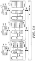
- Figure 1A depicts a multiprocessor digital data processing system constructed in accord with a preferred practice of the invention.
- the illustrated system includes plural central processing units 40A, 40B and 40C coupled, respectively, to associated memory elements (or, caches) 42A, 42B and 42C. Communications between the processing and memory units of each pair are carried along buses 44A, 44B and 44C, as shown.
- the illustrated system further includes memory management element 46 for accessing information-representative signals stored in memory elements 44A, 44B and 44C via buses 48A, 48B and 48C, respectively.
- the central processing units 40A, 40B and 40C each include an access request element, labelled 50A, 50B and 50C, respectively, as well as a post-store element, labelled 51A, 51B and 51C, respectively.
- the access request elements generate signals representative of requests for access to an information stored in the memory elements 42A, 42B and 42C.
- the ownership-request signal representing requests for priority access to an information-representative signal.
- the post-store elements 51A, 51B, 51C generate signals representative of requests for transfer of a copy of a datum, e.g., one which is exclusively owned in the associated processing cell and for which an invalid descriptor is allocated in another processing cell, to other caches.
- access request elements 50A, 50B and 50C and post-store elements 51A, 51B, and 51C comprise a subset of an instruction subset implemented on CPU's 40A, 40B and 40C and described below.
- the memory elements 42A, 42B and 42C include control elements 52A, 52B and 52C, respectively. Each of these control units interfaces a data storage area 54A, 54B and 54C via a corresponding directory element 56A, 56B and 56C, as shown.
- Stores 54A, 54B and 54C are utilized by the illustrated system to provide physical storage space for data and instruction signals needed by their respective central processing units. Thus, store 54A maintains data and control information used by CPU 40A, while stores 54B and 54C maintain such information used by central processing units 40B and 40C, respectively.
- the information signals maintained in each of the stores are identified by unique descriptors which, preferrably, correspond to the signals' system addresses. Those descriptors are stored in address storage locations of the corresponding directory. While the descriptors are considered unique, multiple copies of some descriptors may exist among the memory elements 42A, 4B and 42C where those multiple copies identify copies of the same data element.
- Access request signals generated by the central processing units 40A, 40B and 40C include, along with other control information, an SVA request portion matching the SVA address of the requested information signal.
- the control elements 52A, 52B and 52C respond to access-request signals generated their respective central processing units 40A, 40B and 40C for determining whether the requested information-representative signal is stored in the corresponding storage element 54A, 54B and 54C. If so, that item of information is transferred for use by the requesting processor. If not, the control unit 52A, 52B 52C transmits the access-request signal to said memory management element along lines 48A, 48B and 48C.
- Each cache directory acts as a content-addressable memory. This permits a cache, e.g., 42A, to locate a descriptor for a particular page of SVA space without an iterative search through all of its descriptors.
- Each cache directory is implemented as a 16-way set-associative memory with 128 sets. All of the pages of SVA space are divided into 128 equivalence classes, each associated with a cache directory set. A descriptor for a page can only be stored in the set of a cache directory that corresponds to the page's equivalence class. The equivalence class is selected by SVA[20:14], as discussed in greater detail below. At any given time, a cache can describe no more than 16 pages with the same value for SVA[20:14], since there are 16 elements in each set.
- a processing cell When a processing cell responds to a request for a subpage, it supplies, to the requesting unit, the subpage data, along with certain descriptor fields from the local cache.
- the requestor either copies those fields to its own descriptor area, if it has no other valid subpages, or logically OR's those fields into descriptor fields.
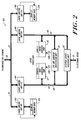
- FIG. 2 depicts a preferred structure for an exemplary processing cell 18A for use in practicing the invention.
- the illustrated processing cell 18A includes a central processing unit 58, coupled with external device interface 60, data subcache 62 and instruction subcache 64 over processor bus 66 and instruction bus 68, respectively.
- Processor 58 comprises any one of several commercially available processors, for example, the Motorola 68000 CPU, adapted to interface subcaches 62 and 64, under control of a subcache co-execution unit acting through data and address control lines 69A and 69B, and further adapted to execute memory instructions as described below.
- processors for example, the Motorola 68000 CPU, adapted to interface subcaches 62 and 64, under control of a subcache co-execution unit acting through data and address control lines 69A and 69B, and further adapted to execute memory instructions as described below.
- Processing cell 18A further includes data memory units 72A and 72B coupled, via cache control units 74A and 74B, to cache bus 76.
- Cache control units 74C and 74D provide coupling between cache bus 76 and processing and data buses 66 and 68.
- bus 78 provides an interconnection between cache bus 76 and the domain(0) bus segment 20A associated with illustrated cell.
- data caches 72A and 72B are dynamic random access memory devices, each capable of storing up to 16 Mbytes of data.
- the subcaches 62 and 64 are static random access memory devices, the former capable of storing up to 256k bytes of data, the latter of up to 256k bytes of instruction information.
- cache and processor buses 76 and 66 provide 64-bit transmission pathways, while instruction bus 68 provides a 64-bit transmission pathway.
- each processing cell includes a subcache that contains .5 MBytes and a cache, e.g., elements 74A and 74B ( Figure 2), that contains 32 MBytes.
- Each cell in turn, can form part of a domain(0) segment having, for example, 15 cells providing and a total of 480 MBytes of storage.
- each domain(0) can form part of domain(1) segment having 32 domain(0) segments providing a total of 15360 Mbytes of storage.
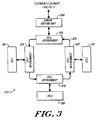
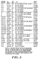
- Figure 3 depicts a preferred configuration for interconnecting groups of processing cells along a unidirectional intercellular bus ring.
- the illustrated group, referred to as "domain(0) segment," 12A comprises processing cells 18A, 18B and 18C interconnected via cell interconnects 22A, 22B and 22c along bus segment 20A.
- Cells residing within the illustrated segment communicate directly with one another over the bus 20A; however, the associated central processing units are not directly interconnected. Instead, interprocessor communications are carried out via the exchange of data and control signals stored in the memory elements.
- the memory management element 46 facilitates this transfer of information.
- domain(0) segment 12A may be attained by reference to the aforementioned European application 88311139.5
- the structure and operation of illustrated bus segment 20A, as well as its interrelationship with cell interconnects 22A, 22B, 22C and 32A is more fully discussed in related European application 88311138.7.
- a multiprocessing system 10 for use with a preferred embodiment of the invention permits access to individual data elements stored within processing cells 18A, 18B, 18C by reference to a unique system virtual address (SVA) associated with each datum.
- SVA system virtual address
- Implementation of this capability is provided by the combined actions of the memory management system 46, the subcaches 62, 64 and the caches 72A, 72B.
- the memory management system 46 includes cache control units 74A, 74B, 74C and 74D, with their related interface circuitry. It will further be appreciated that the aforementioned elements are collectively referred to as the "memory system.”
- Data access requests generated by a processor, e.g., 40A are handled by the local memory element, e.g., 42A, whenever possible. More particularly, a controller, e.g., 74A, 74B, 74C, 74D ( Figure 2), coupled with each memory monitors the cell's internal bus, e.g., 66, and responds to local processor requests by comparing the request with descriptors listed in the corresponding directory. If found, matching data is transmitted back along the internal bus to the requesting processor.
- a controller e.g., 74A, 74B, 74C, 74D ( Figure 2), coupled with each memory monitors the cell's internal bus, e.g., 66, and responds to local processor requests by comparing the request with descriptors listed in the corresponding directory. If found, matching data is transmitted back along the internal bus to the requesting processor.
- the memory management element broadcasts an access-request signal received from the requesting central processing unit to the memory elements associated with the other central processing units.
- the memory management element effects comparison of the SVA of an access request signal with the descriptors stored in the directories 56A, 56B and 56C of each of the memory elements to determine whether the requested signal is stored in any of those elements. If so, the requested signal, or a copy thereof, is transferred via the memory management element 46 to the memory element associated with the requesting central processing unit. If the requested information signal is not found among the memory elements 42A, 42B and 42C, the operating system can effect a search among the system's peripheral devices (not shown) in a manner described below.
- Data movement between processing cells is governed by a protocol involving comparative evaluation of each access request with the access state associated with the requested item.
- the memory management system responds to a request for exclusive ownership of a datum by moving that datum to the memory element of the requesting cell.
- the memory management element allocates physical storage space for the requested item within the requesting cell's data storage area.
- the management element also invalidates the descriptor associated with the requested item within the data store of the remote cell, thereby effecting subsequent deallocation of the physical storage space which had retained the requested item prior to its transfer to the requesting cell.
- the memory management system responds to a request by a first cell for read-only access to datum exclusively owned by a second cell by transmitting a copy of that datum to the first cell while simultaneously designating the original copy of that data, stored in the second cell, as "nonexclusively owned.”
- the system permits an owning cell to disable the copying of its data by providing a further ownership state referred to as the "atomic" state.
- the memory management system responds to requests for data in that state by transmitting a wait, or "transient,” signal to requestors and by broadcasting the requested data over the hierarchy once atomic ownership is relinquished.
- data coherency is maintained through action of the memory management element on memory stores 54A, 54B and 54C and their associated directories 56A, 56B and 56C. More particularly, following generation of an ownership-access request by a first CPU/memory pair (e.g., CPU 40C and its associated memory element 42C), the memory management element 46 effects allocation of space to hold the requested data in the store of the memory element of that pair (e.g., data store 54C of memory element 42C). Concurrent with the transfer of the requested information-representative signal from the memory element in which it was previously stored (e.g., memory element 42A), the memory management element deallocates that physical storage space which had been previously allocated for storage of the requested signal.
- a first CPU/memory pair e.g., CPU 40C and its associated memory element 42C
- the memory management element 46 effects allocation of space to hold the requested data in the store of the memory element of that pair (e.g., data store 54C of memory element 42C).
- the memory management element deallocates that physical
- the system stores information signals DATUM(2) and DATUM(3).
- DATUM(2) and DATUM(3) Corresponding to these data elements are descriptors "car” and “bas,” retained in directory 56B.
- DATUM(2), and its descriptor "bas,” are copies of corresponding elements from cache 42A.
- the illustrated data elements i.e., DATUM(0) through DATUM(3), are accessible -- at least insofar as their existence in the caches 42A, 42B, 42C is concerned -- for request by each of central processing units.
- the memory management element 46 signals the requesting processor that the requested datum resides in memory. Presuming, further, that the request is for read-only access and that DATUM(2) is not held in atomic state, then the memory management element transfers a copy of that datum to cache 42C, associated with CPU(2).
- DATUM(3) is anchored.
- the memory management system 46 noting that the anchor bit associated with the descriptor "car” is set, responds to an access request for DATUM(3) by either of the CPU's 40A, 40C by signalling those processors that the datum does not reside in memory.
- CPU(1) retains full access to DATUM(3), as that CPU accesses the datum directly, without intervention of the memory management system 46.
- Figure 1B illustrates responses of the memory management system 46 following issuance of a request for ownership access to a non-anchored datum.
- the illustration depicts the movement of non-anchored information signal DATUM(0) following issuance of an ownership-access request for that datum by CPU(2).
- the memory management element 46 allocates physical storage space in the store 54C of the memory element partnered with CPU 40C.
- the memory management element 46 then moves the requested information signal DATUM(0) from store 54A, where it had previously been stored, to the requestor's store 54C, while concurrently deallocating that space in store 54A which had previously held the requested signal.
- the memory management element 46 also invalidates the descriptor "foo" in directory 56A, where it had previously been used to identify DATUM(0) in store 54A, and reallocation of that same descriptor in directory 56C, where it will subsequently be used to identify the signal in store 54C.
- Figure 1B also illustrates changes in the anchor state of data stored in the respective caches 42B, 42C. Particularly, as indicated by the absence of parenthesis in the corresponding directory entry, DATUM(3) is not anchored and, accordingly, is available for access by the other central processing units. Conversely, parenthesis surrounding the descriptor "foo" in cache 42C indicate that the associated datum, DATUM(0), is anchored and, thus, unavailable to the other CPU's. As above, CPU 40C can itself access DATUM(0) directly, notwithstanding that its anchor bit is set.
- the anchor bit contained in each descriptor is set by the central processing unit associated with the cache in which that descriptor, as well as the corresponding information-representative signal, is stored.
- CPU 40A sets the anchor bits associated with data in cache 42A:
- CPU 40B sets the anchor bits associated with data in cache 42B;
- CPU 42C set the anchor bits associated with data in cache 42C.
- this anchoring functions are carried out by the functionality labelled "ANCH" in each of the CPU's 40A, 40B, 40C.
- the memory management element 46 includes a mechanism for assigning access state information to the data and control signals stored in the memory elements 42A, 42B and 42C.
- These access states which include the invalid, read-only, owner and atomic states, govern the manner in which data may be accessed by specific processors.
- a datum which is stored in a memory element whose associated CPU maintains priority access over that datum is assigned an ownership state. While, a datum which is stored in a memory element whose associated CPU does not maintain priority access over that datum is assigned a read-only state. Further, a purported datum which associated with "bad" data is assigned the invalid state.
- the memory system stores data in units of pages and subpages. Each individual cache describes 32 Mbytes of SVA space, subdivided into 2048 pages. Pages contain 2 14 (16384) bytes, divided into 128 subpages of 2 7 (128) bytes.
- the memory system allocates storage in the caches, e.g., 72A, 72B ( Figure 2), on a page basis, and each page of SVA space is either entirely represented in the system or not represented at all.
- the memory system shares data between caches in units of subpages.
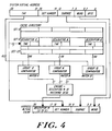
- Each cache directory is made up of descriptors. There is one descriptor for each page of memory in a cache. At a particular time, each descriptor is said to be valid or invalid. If a descriptor is valid, then the corresponding cache memory page is associated with a page of SVA space, and the descriptor records the associated SVA page address and state information. If a descriptor is invalid, then the corresponding cache memory page is logically not in use. There is no explicit validity flag associated with a descriptor; a descriptor may be considered invalid if the anchor and held fields are both clear, and there are no valid subpages present for the SVA page.
- the organization of the cache directory is shown in Figure 4.
- the cache When a reference to an SVA is made, the cache must determine whether or not it has the required information. This is accomplished by selecting a set within the cache, and then examining all the descriptors of that set. SVA[20:14] selects a set. In the general architecture, each of the descriptors in the selected set is simultaneously compared against SVA[63:21]. This teachings provided herein describe a 2 40 byte SVA space, implying a comparison with SVA[39:21]. If one of the elements of the set is a descriptor for the desired page, the corresponding comparator will indicate a match. The index in the set of the matching descriptor, concatenated with the set number, identifies a page in the cache.
- the cache If more than one descriptor matches, the cache signals a multiple_descriptor_match exception. If no descriptor matches, the cache allocates a descriptor and requests data from the interconnect. It is possible that either the allocation or data request will fail, and the cache will indicate an error to the CPU.
- SVA[20:14] The use of SVA[20:14] to select a set is effectively a hash function over SVA addresses.
- System software must assign SVA addresses so that this hash function gives good performance in common cases. There are two important distribution cases: referencing many pages of a single segment and referencing the first page of many segments. This set selector produces good cache behavior for contiguous groups of pages, since 128 contiguous pages will reside in 128 distinct sets. However, this selector will produce poor hashing behavior for many pages with the same value in SVA[20:14].
- System software can avoid the latter situation by varying the logical origin of data within segments. For example, each per-process user stack can be started at a different segment offset.
- Bits [39:21] of an SVA This field identifies the particular page of SVA space specified by the corresponding descriptor. For a given set in a given cell, this field must be unique among all 16 descriptors. Software 'sets' this field when it creates an SVA page. It is also set by software during cache initialization.
- a cache sets this bit flag to one when any subpage of this page undergoes a transition into or out of atomic state because a gsp or rsp instruction was successfully executed. It is also set when a subpage changes from atomic state to transient-atomic state. This flag is not set if a gsp fails because the subpage is already in atomic state or if a rsp fails because the subpage was not in atomic state. This flag is not set if the gsp or rsp fails because descriptor.no_atomic is set. System software sets this flag to zero to indicate that it has noted the atomic state changes. This field is propagated from cache to cache.
- a cache sets this bit flag to one when any data is modified in the page.
- System software sets descriptor.modified to zero to indicate that it has noted the modification of the page. This flag is not set if an attempt to modify data fails because descriptor.no write is set. This field is propagated from cache to cache.
- the cache maintains this field as the current position of the descriptor in its set from Most Recently Used (0) to Least Recently Used (15).
- Software sets the field to indicate that data requests from other caches may not be honored nor may the descriptor be invalidated. Any read or get request from another cache returns unresponded to the requestor, and is treated as if the page were missing.
- This field is set by system software as part of creating or destroying an SVA page, and as part of modifying the page descriptor.
- Software sets the field to indicate that the descriptor may not be invalidated by the cache even if no subpages are present in the cache.
- the subpage state consists of a three-bit state field and a single bit subcached status field. It is set by the cache to record the state of each subpage and to indicate whether or not any portion of the subpage is present in the CPU subcache.
- Descriptor.no_write can be used to implement a copy-on-access scheme, which in turn can be used as an approximation of 'copy-on-write'.
- the pages of the forking process's address space are set to take page_no_write exceptions.
- the child process's address space segments are left sparse.
- descriptor.no_write is cleared for that page. If the parent writes a page before the child has copied it, the page_no_write handler copies the page into the child's address space and then clears descriptor.no write.
- the CPU subcache indicates that the subblock has been modified, but the local cache still show the subpage as unmodified.
- CPU B will send the subblock data from its subcache to the local cache. This can occur because the CPU requires the subcache block for other data, because the CPU is using idle cycles to write-back modified subblocks, or because some other cell has requested the subpage. Then the cell B cache sets the descriptor.modified flag. Throughout this time, descriptor.modified is clear on cell A.
- System software must ensure that the SVA page is really present in the memory system when it attempts to use descriptor information.
- One method of accomplishing this is to always set the page anchor and obtain at least one valid subpage in the local cache.
- software must first obtain every subpage in exclusive state. The anchor prevents any other cache from asynchronously acquiring any subpage already obtained.
- system software clears descriptor.anchor in the local cache. Then other cache request for subpages of that page will again be honored.
- System software also needs to ensure that an SVA page does not really exist in the memory system before it creates the page.
- Software can verify non-presence by setting the page anchor and then attempting to fetch a subpage with exclusive state. If the fetch succeeds, software has lost a race, and the page exists in the memory systems. Otherwise, software can create the page using the mpdw instruction to establish the SVA page address with all subpages owned exclusively. Note that there still needs to be a software interlock against the simultaneous use of mpdw for this purpose.
- each processor e.g., 18A
- instruction subcache 62 Once the instruction subcache 62 has been enabled, all CPU instructions are obtained from the instruction subcache. Most CPU load/store-class instructions operate on data in the subcache, although some operate directly on data in the local cache. Data moves from the local cache to the CPU as the CPU fetches instructions or when the CPU executes (most) load or store instructions. Data moves from the CPU to the cache when the CPU must re-use subcache space or when the local cache requests the data in response to a request from some other cell.
- each subcache 62, 64 describes 256 Kbytes of SVA space.
- the subcaches are based on 64 bit words, like the cache.
- the two sides of the subcache are similar in structure to the cache, but unit sizes differ.
- the subcaches store data in units of blocks and subblocks.
- the subcache is two-way set associative, and have 64 sets. Blocks contain 2 11 (2048) bytes, divided into 2 5 (32) subblocks of 2 6 (64) bytes.
- the CPU allocates subcache space on a block basis; within a block, each subblock may or may not be present in a particular subcache.
- Each subcache directory is made up of subcache descriptors. There is one descriptor for each block of memory in a subcache. A subcache descriptor can be said to be either valid or invalid. It is valid if any subblock within the block is valid. A subcache descriptor can only be valid if the local cache also has a valid descriptor for the same SVA page. Further, the state of each subblock within the block must be no 'stronger' than the state of the corresponding subpage in the local cache.
- each of its subpages is resident in one or more of the caches, e.g., 72A, 72B.
- the descriptor (in that cache) for the containing SVA page records the presence of that subpage in one of several states.
- the state of the subpage in a cache determines two things:
- the states of subpages in caches change over time as programs request operations that require particular states.
- a set of transition rules specify the changes in subpage states that result from processor requests and inter-cache domain communications.
- the CPU obtains the data from the cache. If the local cache does not have the data in the correct state, it communicates over the domains to acquire a copy of the subpage and/or to acquire the necessary state for the subpage. If the cache fails to satisfy the request, it returns an error indication to the processor, which signals an appropriate exception.
- the instruction set includes several different forms of load and store instructions that permit programs to request subpage states appropriate to the expected future data reference pattern of the current thread of control, as well as protocol between different threads of control in a parallel application. This section first describes the states and their transitions in terms of processor instructions and their effect on the caches.
- the basic model of data sharing is defined in terms of three classes of subpage states: invalid, read-only, and owner. These three classes are ordered in strength according to the access that they permit. Invalid states permit no access. Read-only state permits load and instruction-fetch access. There are several owner states: all permit load access and permit the cache to respond to a data request from the interconnect; some permit store access. Only one cache may hold a particular subpage in an owner state at any given time. The cache that holds a subpage in an owner state is called the owner of the subpage. Ownership of each subpage moves from cache to cache as processors request ownership via store instructions and special load instructions that request ownership.
- a subpage When a subpage is not present in a cache, it is said to be in an invalid state with respect to that cache. If a processor, e.g., 40A, requests a load or store to a subpage which is in an invalid state in its local cache, then that cache must request a copy of the subpage in some other state in order to satisfy the data access. There are two invalid states: invalid-descriptor and invalid.
- the local cache When the CPU references a subpage in invalid-descriptor state, the local cache must allocate one of the descriptors (in the correct set) to the SVA. After the descriptor allocation is complete, all subpages in the page have invalid state.
- the local cache When the local cache has a descriptor for a particular page, but a particular subpage is not present in that cache, then that subpage is in invalid state. The local cache will attempt to obtain the subpage data by communicating with other caches.
- read-only state There is only one read-only state: read-only. Any number of caches, e.g., 72A, 72B, may hold a particular subpage in read-only state, provided that the owner of the subpage holds the subpage in non-exclusive state. If the owner of the subpage has any other state(i.e. an exclusive-ownership state, one of: exclusive, atomic, or transient-atomic), then no read-only copies can exist in any cell. The CPU cannot modify a subpage which is in read-only state.
- Non-exclusive and exclusive-ownership There are two basic owner state types: non-exclusive and exclusive-ownership. When a particular cache holds a particular subpage in non-exclusive state, then some other caches may be holding that subpage in read-only state. Programmatically, non-exclusive state is the same as read-only state. The CPU cannot modify a subpage which is in non-exclusive state. Non-exclusive state is basically a book-keeping state used by the memory system; it defines the ownership of the subpage.
- the exclusive-ownership states are exclusive, atomic, and transient-atomic. When a particular cache holds a particular subpage in an exclusive-ownership state, then no other cache may hold a read-only or non-exclusive copy of the subpage. If the local cache has a subpage in an exclusive-ownership state, the CPU can modify subpage data provided that the STT grants write access to the segment and the descriptor.no_write flag is clear.
- Atomic state is a stronger form of ownership than exclusive state. Subpages only enter and leave atomic state as a result of explicit requests by programs.
- atomic state can be used to single-thread access to any subpage in SVA space.
- a processor executes a gsp.nwt (get-subpage, no-wait) instruction to request that a subpage enter atomic state
- the instruction will only complete normally if the subpage is not in atomic state already.
- atomic state on a subpage can be used as a simple lock.
- the lock is locked when the gsp.nwt instruction completes normally by first obtaining the subpage in exclusive state and then changing state from exclusive to atomic.
- the lock is unlocked by executing the rsp (release-subpage) instruction.
- the rsp instruction requires that the subpage exist in some cache with atomic or transient-atomic state.
- the local cache obtains the subpage and then changes the subpage from atomic or transient-atomic state to exclusive state. (If the subpage has transient-atomic state, the operation is more complex, but the effect is programmatically the same.)
- atomic state is associated only with a subpage; there is no association with a particular operating system process (typically a user program) or to a particular cell. It is possible for a process to execute gsp to get a subpage in atomic state and subsequently be switched by system software so that it continues execution on another cell. That process continues execution on the second cell and eventually executes an rsp instruction to release the subpage. Between those two instructions, there will only be a single copy of the subpage in the entire memory system, and it will be in atomic or transient-atomic state. As various processors execute instructions which reference the subpage, that single valid copy will move from cell to cell. It is also possible for a particular process to get atomic state, and another process to release atomic state.
- Atomic state is an additional flag associated with a subpage; it is possible to implement protocols which use atomic state in addition to the data state of the subpage. Just as a protocol which is implemented using only data can have errors, it is possible for an atomic-state protocol to be defective.
- the hardware does not impose any checking on the use of atomic state (beyond access control imposed by the STT and descriptor.no_atomic).
- the gsp.nwt instruction always completes within its defined execution time, but it can succeed or fail (depending upon the current state of the subpage in the memory system).
- a second form of the instruction is gsp.wt (get-subpage, wait), which will not complete until the subpage is obtained in exclusive state and changed to atomic state.
- the gsp.wt instruction relieves the programmer of the burden of determining whether or not the gsp instruction was successful. If the subpage is already in atomic or transient-atomic state when a processor, e.g., 40A, executes gsp.wt, the processor will stall until the subpage is released, obtained by the local cache, and changed back from exclusive state to atomic or transient-atomic state.
- Use of the gsp.wt instruction can reduce the number of messages sent between caches as a cell waits for the opportunity to 'lock the lock'.
- Transient-atomic state is used automatically by the memory system to allow gsp.wt to function efficiently. Its use is entirely transparent to the programmer. If a subpage is in atomic state and another cache executes gsp.wt on that subpage, that subpage enters transient-atomic state in the holding cache. When the subpage is later released with an rsp instruction, the transient-atomic state forces the subpage to be expelled onto the interconnect in a special release state. The releasing caches, e.g., 72A, 72B, changes its own state for the subpage to invalid. Any cache which is executing a gsp will see the subpage and accept it.
- the accepting cache will then be able to complete its gsp instruction and the subpage will enter transient-atomic state in that cache. This operation will happen for each succeeding gsp and rsp until such time as an expelled subpage is not accepted by any other cache. At that time, the cache performing the release will change its subpage state back from invalid state (set when the subpage was released) back to exclusive state.
- the packet with release state will be accepted by a cache whose CPU is performing a load or store instruction.
- the original cache sees that the subpage was accepted, and leaves its subpage in invalid state.
- the accepting cache allows its CPU to execute a single instruction before it retracts the subpage, sets its own subpage state to invalid, and sends the subpage out with release state.
- the cache which was executing the load or store is now the owner of the page, for purposes of this release. As before, if no other cache accepts the data, this cache will change the subpage state to exclusive state and retain ownership.
- a gsp.wt instruction may wait until the subpage is released.
- the instruction may be interrupted by various peripheral controller interface ("XIU") signals; when such an event occurs, the CCUs abandon the attempt to gain atomic access. If the subpage is released in the interim, and there is no other requestor, it will change from transient-atomic state release state and finally to exclusive state. Since the typical system software action is to service the interrupt and restart the interrupted instruction, the CCU will again issue the request. It may succeed or be forced to wait, as before.
- XIU peripheral controller interface
- the basic mechanism by which data moves from some owning cache to other caches is by instruction fetches and the execution of load and store instructions by the processors local to those other caches.
- the different load and prefetch instructions permit programs to request that their local cache acquire read-only or an exclusive-ownership state; a store instruction always requires that the subpage have an exclusive-ownership state.
- a cache may acquire a read-only copy of a subpage as it passes by on the interconnect.
- the post-store-subpage (pstsp) instruction broadcasts a read-only copy of a subpage to all interested caches.
- the owning cache may send ownership state on the interconnect as part of recombining a later.
- Instruction fetches and load instructions can result in the local cache requesting a read-only copy of the subpage. This request is answered by the cache which owns the subpage. If the owning cache has the subpage in non-exclusive state, it supplies a read-only copy to the requesting cache, but does not change its own state. If the owning cache has the subpage in exclusive state, it changes its own subpage state to non-exclusive and then supplies the read-only copy to the requestor. If the owning cache has the subpage in atomic or transient-atomic state, it supplies the subpage with that state and invalidates its own copy.
- a cache When a cache acquires a subpage with an exclusive-ownership state in order to satisfy a store instruction, it does not grant ownership or a read-only copy to another cache until the store instruction is complete.
- This rule provides the strongly ordered nature of the memory system, in that it ensures readers of a memory location see modifications in the order that they are made.
- a subpage When a subpage is in atomic state it may change to transient-atomic state, but it will never change to any other state as a result of any load or store instruction. If some other cache requests the subpage, it will always obtain the subpage in atomic or transient-atomic state. After the subpage has been released to exclusive state, the transitions between exclusive and non-exclusive state may again occur, and read only copies may exist when the subpage is owned non-exclusively.
- subpage atomic state is used purely as a lock.
- the data in the subpage is not relevant.
- Some of the more sophisticated forms of synchronization mechanisms make use of the data in a subpage held in atomic state.
- One technique is to use atomic state on a subpage as a lock on the data in that subpage. Programs take one or more subpages into atomic state, manipulate their contents, and release them.
- Each cache maintains LRU state for all of the resident pages.
- the LRU data is maintained separately for each of the 128 sets of the descriptor associative memory, and orders the 16-pages in the set according to their approximate time of last reference.
- Each cache maintains an LRU to MRU ordering of the descriptors in each set. The ordering is maintained in descriptor.LRU_priority.
- Each of the descriptors in a set has a value from 0 (MRU) to 15 (LRU) in descriptor.LRU_priority.
- the cache proceeds in order through as many of the following actions as needed to find a usable descriptor:
- the cache attempts to identify a descriptor which contains only read-only copies of subpages. It searches from LRU to MRU, looking for any page which has:
- a processor passes load and store instructions to its local cache as requests when the subblock containing the referenced address is not present in the subcache in the required state.
- the different types of load and store instructions pass information to the local cache about the access patterns of the following instructions. For example, if the sequence of the instructions is a load followed by a store, and the subpage containing the data item is not yet resident in the local cache, it is more efficient to acquire ownership for the load than to get a read-only copy for the load instruction and then communicate over the domains a second time to acquire ownership for the store instruction.
- the state of subblocks in the subcaches does not always reflect the state of the corresponding subpage in the cache.
- the instruction subcache always obtains a read-only copy of data.
- the data subcache may hold a subblock in read-only or exclusive state.
- the subcache can only have exclusive state if the cache has an exclusive-ownership state and descriptor.no_write is not set. (The subcache does not distinguish between exclusive, atomic, and transient-atomic subpage states).
- the CPU can execute store instructions by placing the new date in the subcache.
- the owning cache When a request for a subpage arrives from another cache, the owning cache must respond. If any part of the subpage is in the data subcache, the local cache must ensure that it obtains any modifications which might be present only in the subcache. The cache also causes the CPU to change subcache state for the subblock to read-only or invalid, depending upon the request. In certain cases, the cache will also ensure that the instruction subcache invalidates its read-only copy of the subpage.
- load and store instructions are described below. Each description begins with a brief summary of the semantics of the instruction, and continues with an overview of subcache and cache actions.
- the program will continue a pattern of reading data. The minimum amount of work is done to obtain data. If the containing subblock is subcached, it is used directly. If the local cache does not have the subpage, it obtains a copy. The local cache supplies the subblock to the subcache with exclusive or read-only state, as appropriate.
- the program will write the subblock in the following instructions, and exclusive state is preferable to any other state.
- a program would use this when the data was expected to have little sharing, or when a series of writes was upcoming. This can reduce the number of interconnect messages required before the CPU can modify data.
- a particular example of the use of load (exclusive) is per-program data such as stacks.
- load exclusive
- per-program data such as stacks.
- there will by no read-only copies of such data since the only copy will be the one in use by the program.
- the new processor's local cache will have no copy, and the old processor's local cache will continue to hold the subpage in an exclusive-ownership state.
- the program used load read-only
- the local cache acquires the subpage in read-only state (unless the subpage is in atomic or transient-atomic state, in which case that state is acquired).
- the subsequent store requires the cache to make another interconnect request (to obtain an exclusive-ownership state) before any CPU data modification can occur.
- the minimum amount of work is done to obtain data. If the subblock is already present in the subcache, it is used directly. If the local cache does not have the subpage, it requests the subpage in an exclusive-ownership state. When the local cache has the subpage, the subblock is supplied to the CPU in read-only or exclusive state, as appropriate.
- subcache state is unchanged; data is written to the subcache.
- the subcache must have the subblock in exclusive state. As necessary, the subcache will request exclusive state from the local cache, and the local cache will request an exclusive-ownership state from the interconnect.
- the programmer uses the exclusive and read_only designations according to the expected reference pattern, as documented for ld . However, the number of references to the subblock is expected to be small, and the subcache should not be disturbed while fetching this data.
- the data is present in the subcache, it is used directly. If the local cache does not have the subpage, it obtains a copy. The CPU obtains a copy of the data and loads the destination registers.
- the number of references to the subblock is expected to be small (typically one), and the subcache should not be disturbed while storing this data.
- the subcache state is unchanged and data is written to the subcache. If the subpage is subcached in read-only state it is immediately invalidated. The CPU supplies the data to the local cache. If the cache does not have the subpage in an exclusive-ownership state, it requests it from the interconnect.
- the subpage atomic instructions are the program interface to the get and release operations described above. These instructions exist in several forms to permit precise tuning of parallel programs.
- Get subpage requests that a subpage be set into atomic state. For both forms of the get subpage instruction, if the subpage is not in atomic state in any cache, then the local cache acquires it in atomic state.
- the @MEM condition code indicates the success or failure of the attempt; the instruction will trap instead of changing @MEM if the trap option is present in the instruction and the subpage is already atomic.
- the gsp.wt instruction form causes the cache to stall the CPU until the subpage can be obtained in atomic state. This reduces the amount of interconnect traffic if the program must obtain atomic state before it can proceed. If the subpage is already atomic in any cache (including the local cache), the instruction waits until the subpage is released. The local cache then acquires the subpage in atomic state. The @MEM condition is always changed to indicate success.
- Release subpage is used to remove a subpage from atomic state. If the subpage is not present in the local cache, it is first requested in via the interconnect. Once the local cache has exclusive ownership, rsp proceeds. If the subpage is not in atomic state then release subpage does not change the subpage state. In this situation, the CPU will trap if the trap modifier is present for the instruction. If the subpage is in atomic state, it is changed to exclusive state. If the subpage is in transient-atomic state, it is changed to exclusive state and expelled onto the interconnect so that any waiting cell may acquire atomic state.
- Post-store subpage allows the program to expel a read-only copy of a subpage onto the interconnect. All caches with descriptors for the page will take a copy of the data. This instruction can be used to broadcast data as part of completing some operation, reducing the probability that some other cache will have to make a read request on the interconnect when it needs to use the data.
- Prefetch Subpage requests that a copy of a subpage be acquired on the local cache in a specified state.
- the instruction can request read-only or exclusive state. A subsequent reference to the subpage blocks until the prefetch subpage has completed.
- a cache forces its local processor to remove a subpage from subcache in order to invalidate the subpage in response to a request from another cache.
- Figure 5 provides a specification of processor load/store class instructions and the state of the addressed subblock in the subcache. If a hit is indicated, the process or uses the subcache directly for loading or storing. If a miss is indicated, the process or communicates with he local cache.
- the memory system is designed to support a virtual memory system with automatic data sharing and LRU maintenance.
- software can take explicit control of the memory system for special applications.
- system software can prevent the cache from ever moving or destroying a page to make room for another page.
- the system software can then handle exceptions or perform explicit destroys as needed to multiplex each cache's memory.
- the memory system can configured as a shared memory multiprocessor.
- the memory system can be configured to emulate more loosely coupled message-oriented architectures. Messages can be passed by references to special SVA ranges. Manual control of the memory system can be used to enforce a specific memory model more closely.
- Control operation permit the processor, e.g., 40A, to directly manipulate the memory system.
- the data movement control instructions move pages and subpages of data from cache to cache in the system.
- the page state control instructions manipulate page descriptors.
- CPU instructions result in cache commands which execute synchronously or asynchronously, depending upon the command.
- a CPU cache instruction occupies an entry in the cache PRT (a hardware table) while it is in progress.
- the PRT has four entries, so a maximum of four cache instructions may execute in parallel.
- Most CPU instructions result in assignment of a PRT entry which remains in use until the request is satisfied, providing synchronous behavior. For example, load/store instructions execute synchronously, so that certain software-controlled exceptions (such as missing page or unwriteable page) can be predictably resolved.
- the pcsp (prefetch-cache-subpage) and pstsp (post-store-subpage) instructions operate asynchronously, as described in following subsections.
- Synchronous errors typically result in the CPU executing the trap sequence; further information can be obtained from CCU control locations, as described in the 'Control Locations' chapter.
- Asynchronous errors result from actual hardware errors or are provoked by a request from some other cache. Such errors are reported by memory-system interrupts.
- the prefetch instructions request that a copy of a subpage be acquired on the local cache in a specified state.
- Pcsp prefetches a subpage.
- the cache allocates a PRT entry when this instruction is detected. If the subpage is already present, the PRT entry is freed and the pcsp completes. Otherwise, the cache issues a request, and then indicates instruction completion to the CPU, which proceeds asynchronously. When the message returns as a request or response, the cache accepts data (if present), and frees the PRT entry. There is no indication to the CPU that the data has arrived.
- the pstsp instruction requests that a copy of a subpage be circulated on the interconnect so that any caches having a descriptor for the containing page may acquire a read-only copy of the subpage.
- pstsp references a subblock within a subpage. If the subblock is subcached with exclusive state and is modified in the subcache, the CPU requests a post-store action from the local cache; otherwise, the pstsp instruction has no effect.
- the cache allocates a PRT entry, and requests the subpage data from the CPU.
- the cache then submits the post-store message to the interconnect, frees the PRT entry, and indicates instruction completion to the CPU.
- the CPU proceeds asynchronously. When the message returns to the issuing cache, it is discarded.
- the mfsva instructions permits system software to fetch a subpage in read-only or exclusive-ownership state, specifying the SVA location of the subpage. This saves system software the effort of establishing a DSTT translation, as is required by pcsp .
- the mflsp instruction causes the cache to ensure that the specified subpage is not subcached in the local CPU. If the subpage is in invalid-descriptor state or invalid state, no descriptor is allocated and the subpage is not requested via the interconnect.
- the mrcsp instruction allows system software to reduce the number of active descriptors for a page by causing ownership to migrate to another cache. Unlike the background recombine activity of the cache, this instruction is not controlled by cache configuration parameters.
- the page state control instructions operate on individual pages of SVA space.
- the mpsa instruction provides an anchored descriptor in the local cache for an SVA page. If the descriptor already existed prior to the mpsa , its anchor flag is set. Otherwise, the cache allocates a descriptor and then sets the anchor flag. Page state control operations require that an anchored descriptor for the SVA page be present on the local cache.
- the mpdw instruction is used to create and destroy SVA pages, and to change descriptor flags of existing SVA pages.
- mpdw requires that system software first obtain an anchored descriptor for the page, using the mpsa instruction. The following discussion assumes that an anchored descriptor exists on the local cache.
- the SVA page now exists, although its data values are undefined.
- Software must initialize the page using store instructions or I/O before allowing the user to reference the page. For this reason, software will typically create a page at an SVA location inaccessible to user programs, initialize the page data, and then change the address of the SVA page as described below.
- the page is released for general use by executing an mpdw instruction which clears the anchor.
- system software After the mpsa , system software must obtain all subpages in exclusive state. This is done using mfsva instructions. Software then executes mpdw specifying that all subpages should be changed to invalid state. This instruction causes a message to be sent on the interconnect so that any interested ring members may note the destruction of the page. The SVA page is destroyed by this operation. Software releases the descriptor for reuse by executing a second mpdw which clears the anchor.
- the mpdw instruction is used to change various fields in a local descriptor. It can set or clear the modified, atomic_modified, no_write, no atomic, and held fields and can clear the anchor field. mpdw can also change the tag, and thus the SVA space address associated with the descriptor. (Since the index of the descriptor forms part of the SVA, the new tag is in the same cache set, by definition.)
- descriptor.no_write include: prevention of inadvertent modification of certain data; support for copy_on_write/copy_on_access protocols; debugger watchpoints.
- no_write is set and remains set.
- system software can respond by making a copy of the page available to the other users and then clearing no write (see the system programming note 'Copy on Access', earlier in this chapter). Software can make this change local or global; in the former case, no write faults may continue to occur on other cells which reference the page.
- debugger watchpoints are intended to detect the modification of a particular region of context address space (e.g. find out where a global variable is being destroyed).
- System software can implement this by setting no_write for the page, and trapping every modification attempt. For modifications outside the watched range, system software can anchor the page, clear no_write, modify the data, unsubcache the data, set no_write, and proceed. (It is also possible to implement watchpoint support by making global changes to no_write.)
- the mfpl instruction searches a specified set in the LRU space of the cache for a descriptor that matches a specified set of criteria.
- the search begins with the descriptor at LRU position 15, and proceeds upward until the criteria are met.
- the cache To ensure correct operation, the cache must know when a subpage is also present in a CPU subcache. This permits the cache to request subcache invalidation when some request from the interconnect (or even the local CPU) requires a subpage state change.
- the CPU communicates with the cache when it changes subcaching status.
- the cache does not maintain per-subcache information.
- the same subpage of SVA space must not simultaneously appear in both subcaches. In general, this results in a system software restriction that the same SVA region cannot be used as both instructions and data. Self-modifying programs or programs where code and data are part of the same context address segment are not supported.
- system software To read an instruction as data, system software must:
- system software To write an instruction subpage as data, system software must:
- Instruction pages are typically pure and do not need to be written from SVA space to an I/O device as part of system SVA space management. Before writing an instruction page, system software must:
- a digital data processing system having a plurality of processing cells and a memory management element that moves exclusive data copies from cell to cell in response to access requests generated by the cells, and that permits the processing cells to "anchor" selected data to cause other cells which request that data from to be signalled that it does not reside in memory.
- Other aspects of the invention provide funtionality that permits central processing units owning data elements to broadcast copies of those elements to other processors that previously retained copies, e.g., read-only, of the same data.
- a multiprocessing system constructed in accord with the invention features improved data coherency, reduced latency and bus contention, as well as unlimited scalability.
Landscapes
- Engineering & Computer Science (AREA)
- Theoretical Computer Science (AREA)
- Physics & Mathematics (AREA)
- Software Systems (AREA)
- General Engineering & Computer Science (AREA)
- General Physics & Mathematics (AREA)
- Computer Hardware Design (AREA)
- Quality & Reliability (AREA)
- Mathematical Physics (AREA)
- Memory System Of A Hierarchy Structure (AREA)
- Multi Processors (AREA)
- Hardware Redundancy (AREA)
Claims (18)
- Digitales Datenverarbeitungssystem, das aufweist:eine Speichereinrichtung (54A, 54B, 54C), die derart konfiguriert ist, daß sie zumindest ein Datenelement speichert,zumindest einen ersten und einen zweiten Prozessor (40A, 40B, 40C), welche jeweils dafür konfiguriert sind, daß sie eine Zugriffsanforderung für das Anfordern eines Zugriffs auf das zumindest eine Datenelement, welches in der Speichervorrichtung abgelegt ist, erzeugen, undSpeicherverwaltungseinrichtungen (46, 52A, 52B, 52C, 56A, 56B, 56C), die dafür konfiguriert sind, daß sie Zugriffsanforderungen von dem ersten und zweiten Mikroprozessor erhalten, wobei die Speicherverwaltungseinrichtungen weiterhin dafür konfiguriert sind, daß sie:in einem ersten Modus als Antwort auf eine Zugriffsanforderung, die von irgendeinem der Mikroprozessoren erzeugt wurde, dem jeweiligen Prozessor, der die Zugriffsanforderung erzeugt hat, signalisieren, daß das zumindest eine Datenelement in der Speichereinrichtung gespeichert ist, undin einem zweiten Modus als Antwort auf eine Zugriffsanforderung, die von einem der Prozessoren erzeugt wurde, diesem einen Prozessor signalisieren, daß das zumindest eine Datenelement in der Speichereinrichtung gespeichert ist, und als Antwort auf eine Zugriffsanforderung, die von einem anderen der Prozessoren erzeugt wurde, diesem anderen der Prozessoren nicht signalisieren, daß das zumindest eine Datenelement in der Speichereinrichtung gespeichert ist.
- Digitales Datenverarbeitungssystem nach Anspruch 1, wobei die Speicherverwaltungseinrichtung einen Ankerindikator beinhaltet zur Identifizierung bzw. Bestimmung eines Zugriffsmodus von den besagten ersten oder zweiten Zugriffsmodi, welcher dadurch in Verbindung mit der Reaktion auf Zugriffsanforderungen verwendet werden soll, die durch die Prozessoren erzeugt wurden.
- Digitales Datenverarbeitungssystem nach Anspruch 1 oder 2, wobei die Speichereinrichtung ein erstes und ein zweites Speicherelement (54A, 54B, 54C) aufweist, wobei das erste Speicherelement mit dem ersten Prozessor zugeordnet ist und das zweite Speicherelement mit dem zweiten Prozessor zugeordnet ist.
- Digitales Datenverarbeitungssystem nach Anspruch 3, wobei die Speicherverwaltungseinrichtung weiterhin dafür konfiguriert ist, daß sie das mindestens eine Datenelement in einem der Speicherelemente gespeichert bzw. abgelegt wird.
- Digitales Datenverarbeitungssystem nach Anspruch 4, wobei die Speicherverwaltungseinrichtung weiterhin dafür konfiguriert ist, das zumindest eine Datenelement ausschließlich in einem der Speicherelemente abzulegen.
- Digitales Datenverarbeitungssystem nach Anspruch 5, wobei die Speicherverwaltungseinrichtung weiterhin dafür konfiguriert ist, daß sie selektiv:in dem ersten Zugriffsmodus,als Antwort auf eine Zugriffsanforderung, die von irgend einem der Prozessoren erzeugt wurde, dem jeweiligen Prozessor, der die Zugriffsanforderung erzeugte, signalisiert, daß das zumindest eine Datenelement in der Speichereinrichtung gespeichert ist, undin dem zweiten Zugriffsmodus,als Antwort auf eine Zugriffsanforderung, die von einem der Prozessoren erzeugt wurde, der mit dem Speicherelement verbunden ist, in welchem das Datenelement ausschließlich gespeichert wird, diesem Prozessor signalisiert, daß das mindestens eine Datenelement in der Speichereinrichtung abgelegt bzw. gespeichert ist undals Antwort auf eine Zugriffsanforderung, die durch einen der Prozessoren erzeugt wurde, der nicht mit dem Speicherelement verbunden ist, in dem das Datenelement ausschließlich abgelegt wird, diesem Prozessor nicht signalisiert, daß das mindestens eine Datenelement nicht in der betreffenden Speichereinrichtung abgelegt ist.
- Digitales Datenverarbeitungssystem nach einem der vorhergehenden Ansprüche, wobei die Datenverwaltungseinrichtung einen Ankerindikator beinhaltet, der dafür konfiguriert ist, einen der ersten und zweiten Zugriffsmodi zu bestimmen, der dadurch in Verbindung mit der Erwiderung auf Zugriffsanforderungen, die durch die Prozessoren erzeugt wurden, verwendet werden sollen.
- Digitales Datenverarbeitungssystem nach Anspruch 7, wobei die Speicherverwaltungseinrichtung beinhaltet:ein Speicherverzeichnis (56A, 56B, 56C), das mindestens mit dem einen Speicherelement verbunden ist, in dem das mindestens eine Datenelement ausschließlich abgelegt wird, wobei das Speicherverzeichnis den Ankerindikator beinhaltet, undeinen Kontroller (52A, 52B, 52C), der dafür konfiguriert ist, als Antwort auf eine Zugriffsanforderung, die durch die Prozessoren erzeugt wurde, die einen Zugriff auf das zumindest eine Datenelement anfordern, den Zugriffsmodus, der durch den Ankerindikator angezeigt wird, zu bestimmen und die Zugriffsanforderung durchzuführen, wie es durch den Zugriffsmodus, den jeweiligen Prozessor, der die Zugriffsanforderung erzeugt hat, und das Speicherelement, in dem das mindestens eine Datenelement gespeichert wird, bestimmt wird.
- Digitales Datenverarbeitungssystem nach Anspruch 7 oder 8, wobei der eine der Prozessoren, der mit dem Speicherelement verbunden ist, in dem das mindestens eine Datenelement gespeichert wird, weiterhin dafür konfiguriert ist, den Ankerindikator in einen solchen Zustand zu versetzen, der einen von dem ersten und zweiten Zugriffsmodus identifiziert.
- Digitales Datenverarbeitungssystem nach einem der Ansprüche 1 bis 9, wobei mindestens einer der Prozessoren weiterhin dafür konfiguriert ist, den Zugriffsmodus zu bestimmen.
- Digitales Datenverarbeitungssystem nach einem der vorherigen Ansprüche, das aufweist:mehrere Verarbeitungsspeicherzellen, wobei jede einen Prozessor beinhaltet, der mit einem assoziierten Speicherelement verbunden ist, wobei jedes Speicherelement in der Lage ist, das zumindest eine Datenelement zu speichern,zumindest einen ersten Prozessor, der Einrichtungen zur Erzeugung eines Besitzanforderungssignals, das eine Anforderung eines Vorrangszugriffs auf ein Datenelement darstellt,wobei die Speicherverwaltungseinrichtung eine Speicherkohärenzeinrichtung beinhaltet, die auf die Besitzanforderungssignale reagiert, für die exklusive Zuordnung von physikalischem Speicherplatz innerhalb des Speicherelements, das mit dem ersten Prozessor verbunden ist, für ein erstes angefordertes Datenelement und für die Speicherung dieses Datenelements darin, wobei das erste Datenelement eines ist für das physikalischer Speicherplatz in dem Speicherelement, welches mit einem zweiten Prozessor verbunden ist, zugeordnet wurde, undzumindest der erste Prozessor eine Nachspeicherungseinrichtung beinhaltet für das Bewirken einer Übertragung einer Kopie des Datenelements zu dem Speicherelement, welches mit dem zweiten Prozessor verbunden ist.
- Verfahren zum Betrieb eines digitalen Datenverarbeitungssystems mit Multiprozessoren des Typs mit mindestens einem ersten und einem zweiten Prozessor (40A, 40B, 40C), Speicherverwaltungseinrichtungen (46, 52A, 56A) und Speichereinrichtungen (54A, 54B, 54C) für die Speicherung mindestens eines Datenelements, wobei das Verfahren die Schritte aufweist:Erzeugen einer Zugriffsanforderung innerhalb eines der Prozessoren, der einen Zugriff auf das mindestens eine Datenelement anfordert, undwobei die Speicherverwaltungseinrichtung selektiv in der Weise arbeitet, daß:in einem ersten Modus als Antwort auf eine Zugriffsanforderung, die von irgend einem der Prozessoren erzeugt wurde, dem jeweiligen Prozessor, der die Zugriffsanforderung erzeugt hat, signalisiert wird, daß das mindestens eine Datenelement in der Speichereinrichtung gespeichert ist, oderin einem zweiten Modus als Antwort auf eine Zugriffsanforderung, die von einem bestimmten der Prozessoren erzeugt wurde, dem einen der Prozessoren signalisiert wird, daß das mindestens eine Datenelement in der Speichereinrichtung gespeichert ist, und als Antwort auf eine Zugriffsanforderung, die von irgend einem anderen der Prozessoren erzeugt wurde, dem anderen der Prozessoren nicht signalisiert wird, daß das mindestens eine Datenelement in der Speichereinrichtung abgelegt ist.
- Verfahren nach Anspruch 12, wobei der erste oder zweite Zugriffsschritt auf Basis des Zustands eines Ankerindikators ausgeführt wird.
- Verfahren nach Anspruch 12 oder 13, wobei die Speichereinrichtung erste und zweite Speicherelemente aufweist, wobei das erste Speicherelement mit dem ersten Prozessor verbunden ist und das zweite Speicherelement mit dem zweiten Prozessor verbunden ist, und das mindestens eine Datenelement ausschließlich in einem der Speicherelemente gespeichert wird, und die Speicherverwaltungseinrichtung in der Weise arbeitet, daß:in dem ersten Modus als Antwort auf eine Zugriffsanforderung, die von irgend einem der Prozessoren erzeugt wurde, dem jeweiligen Prozessor, der die Zugriffsanforderung erzeugt hat, signalisiert wird, oderin dem zweiten Modusals Antwort auf eine Zugriffsanforderung, die von dem jeweiligen der Prozessoren erzeugt wurde, der mit dem Speicherelement verbunden ist, in dem das Datenelement ausschließlich gespeichert ist, dem Prozessor signalisiert wird, daß das mindestens eine Datenelement in dem Speicher gespeichert ist, undals Antwort auf eine Zugriffsanforderung, die von einem der Prozessoren erzeugt wurde, der nicht mit dem Speicherelement verbunden ist, in dem das Datenelement ausschließlich gespeichert ist, dem Prozessor signalisiert wird, daß das mindestens eine Datenelement nicht in dem Speicher abgelegt ist.
- Verfahren nach Anspruch 14, wobei der erste oder zweite Zugriffsschritt auf Basis des Zustandes eines Ankerindikators ausgeführt wird.
- Verfahren nach Anspruch 15, wobei der Prozessor, der mit dem Speicherelement verbunden ist, in dem das mindestens eine Datenelement gespeichert ist, die Ankeranzeige konditioniert, um einen von den ersten oder zweiten Zugriffsschritten zu identifizieren, welcher wahlweise ausgeführt werden soll.
- Verfahren nach einem der Ansprüche 12 bis 15, wobei zumindest ein Prozessor die Ankeranzeige konditioniert, um einen, den ersten oder den zweiten, Zugriffsschritt zu bestimmen, der wahlweise ausgeführt werden soll.
- Verfahren nach einem der Ansprüche 12 bis 17 für ein digitales Datenverarbeitungssystem des Typs mit mehreren Verarbeitungsspeicherzellen, die jeweils einen Prozessor beinhalten, der mit einem zugeordneten Speicherelement verbunden ist, wobei jedes Speicherelement in der Lage ist, mindestens ein Datenelement zu speichern, wobei das Verfahren weiterhin aufweist:Erzeugen eines Besitzanforderungssignals zumindest innerhalb eines ersten Prozessors, das eine Anforderung nach einem Vorrangszugriff auf das Datenelement darstellt,Reagieren auf das Besitzanforderungssignal für die exklusive Zuweisung von physikalischem Speicherplatz innerhalb des Speicherelements, das mit dem ersten Prozessor verbunden ist, für ein erstes angefordertes Datenelement und für die Speicherung des Datenelements darin,Erzeugen eines read-only-Anforderungssignals mindestens innerhalb eines zweiten Prozessors, das eine Anforderung nach einem zweitrangigen Zugriff zu dem ersten Datenelement darstellt,Reagieren auf das read-only-Anforderungssignal für die Übertragung einer Kopie des ersten Datenelements zu dem Speicherelement, das mit dem zweiten Prozessor verbunden ist, undselektives Übertragen einer Kopie des ersten Datenelements von dem Speicherelement, das mit dem ersten Prozessor verbunden ist, zu dem Speicherelement, das mit dem zweiten Prozessor verbunden ist.
Applications Claiming Priority (2)
| Application Number | Priority Date | Filing Date | Title |
|---|---|---|---|
| US07/370,287 US5251308A (en) | 1987-12-22 | 1989-06-22 | Shared memory multiprocessor with data hiding and post-store |
| US370287 | 1989-06-22 |
Publications (3)
| Publication Number | Publication Date |
|---|---|
| EP0404560A2 EP0404560A2 (de) | 1990-12-27 |
| EP0404560A3 EP0404560A3 (de) | 1992-08-05 |
| EP0404560B1 true EP0404560B1 (de) | 2000-08-09 |
Family
ID=23459010
Family Applications (1)
| Application Number | Title | Priority Date | Filing Date |
|---|---|---|---|
| EP90306777A Expired - Lifetime EP0404560B1 (de) | 1989-06-22 | 1990-06-21 | Multiprozessorsystem und Verfahren |
Country Status (5)
| Country | Link |
|---|---|
| EP (1) | EP0404560B1 (de) |
| JP (1) | JP3103581B2 (de) |
| AT (1) | ATE195382T1 (de) |
| CA (1) | CA2019300C (de) |
| DE (1) | DE69033601T2 (de) |
Families Citing this family (11)
| Publication number | Priority date | Publication date | Assignee | Title |
|---|---|---|---|---|
| US5761413A (en) * | 1987-12-22 | 1998-06-02 | Sun Microsystems, Inc. | Fault containment system for multiprocessor with shared memory |
| US5313647A (en) * | 1991-09-20 | 1994-05-17 | Kendall Square Research Corporation | Digital data processor with improved checkpointing and forking |
| CA2078312A1 (en) * | 1991-09-20 | 1993-03-21 | Mark A. Kaufman | Digital data processor with improved paging |
| CA2078315A1 (en) * | 1991-09-20 | 1993-03-21 | Christopher L. Reeve | Parallel processing apparatus and method for utilizing tiling |
| US5245563A (en) * | 1991-09-20 | 1993-09-14 | Kendall Square Research Corporation | Fast control for round unit |
| CA2078311A1 (en) * | 1991-09-23 | 1993-03-24 | Sun Microsystems, Inc. | Fault containment system for multiprocessor with shared memory |
| CA2073516A1 (en) * | 1991-11-27 | 1993-05-28 | Peter Michael Kogge | Dynamic multi-mode parallel processor array architecture computer system |
| TW567695B (en) * | 2001-01-17 | 2003-12-21 | Ibm | Digital baseband system |
| JP2005250830A (ja) * | 2004-03-04 | 2005-09-15 | Hitachi Ltd | プロセッサおよび主記憶共有マルチプロセッサ |
| US10542120B2 (en) * | 2016-11-10 | 2020-01-21 | Microsoft Technology Licensing, Llc | Wirelessly providing operating system specific features |
| JP2020198044A (ja) * | 2019-06-05 | 2020-12-10 | 富士通株式会社 | 並列処理装置 |
Family Cites Families (7)
| Publication number | Priority date | Publication date | Assignee | Title |
|---|---|---|---|---|
| US4622631B1 (en) * | 1983-12-30 | 1996-04-09 | Recognition Int Inc | Data processing system having a data coherence solution |
| US4755930A (en) | 1985-06-27 | 1988-07-05 | Encore Computer Corporation | Hierarchical cache memory system and method |
| IT1184013B (it) * | 1985-12-13 | 1987-10-22 | Elsag | Memoria ad elevata capacita accessibile a diverse agenti |
| US4811216A (en) * | 1986-12-22 | 1989-03-07 | American Telephone And Telegraph Company | Multiprocessor memory management method |
| JP3023425B2 (ja) * | 1987-10-09 | 2000-03-21 | 株式会社日立製作所 | データ処理装置 |
| CA1320003C (en) | 1987-12-22 | 1993-07-06 | Steven J. Frank | Interconnection system for multiprocessor structure |
| US5055999A (en) | 1987-12-22 | 1991-10-08 | Kendall Square Research Corporation | Multiprocessor digital data processing system |
-
1990
- 1990-06-19 CA CA002019300A patent/CA2019300C/en not_active Expired - Fee Related
- 1990-06-21 EP EP90306777A patent/EP0404560B1/de not_active Expired - Lifetime
- 1990-06-21 DE DE69033601T patent/DE69033601T2/de not_active Expired - Fee Related
- 1990-06-21 AT AT90306777T patent/ATE195382T1/de active
- 1990-06-22 JP JP02163026A patent/JP3103581B2/ja not_active Expired - Fee Related
Also Published As
| Publication number | Publication date |
|---|---|
| JP3103581B2 (ja) | 2000-10-30 |
| JPH03129454A (ja) | 1991-06-03 |
| ATE195382T1 (de) | 2000-08-15 |
| CA2019300A1 (en) | 1990-12-22 |
| CA2019300C (en) | 2001-06-12 |
| EP0404560A2 (de) | 1990-12-27 |
| EP0404560A3 (de) | 1992-08-05 |
| DE69033601D1 (de) | 2000-09-14 |
| DE69033601T2 (de) | 2001-05-03 |
Similar Documents
| Publication | Publication Date | Title |
|---|---|---|
| US5251308A (en) | Shared memory multiprocessor with data hiding and post-store | |
| EP0593100B1 (de) | Multiprozessor-Digitaldatenverarbeitungssystem und Verfahren zum Betreiben dieses Systems | |
| US5313647A (en) | Digital data processor with improved checkpointing and forking | |
| EP0539012B1 (de) | Verbesserter Digitalprozessor mit verteiltem Speichersystem | |
| US5341483A (en) | Dynamic hierarchial associative memory | |
| EP0458553B1 (de) | Schalter und Verfahren zum Verteilen von Paketen in Netzwerken | |
| EP0856796B1 (de) | Gemeinsame Speicherbenutzung mit variablen Blockgrössen für symmetrische Multiporzessor-Gruppen | |
| US5524212A (en) | Multiprocessor system with write generate method for updating cache | |
| US20110208894A1 (en) | Physical aliasing for thread level speculation with a speculation blind cache | |
| EP0404560B1 (de) | Multiprozessorsystem und Verfahren | |
| US5875468A (en) | Method to pipeline write misses in shared cache multiprocessor systems | |
| EP0533447B1 (de) | Rechner für digitale Daten mit Seitenaustausch | |
| US6925551B2 (en) | Method, apparatus and system for accessing a global promotion facility through execution of a branch-type instruction | |
| US6842847B2 (en) | Method, apparatus and system for acquiring a plurality of global promotion facilities through execution of an instruction | |
| EP0458552B1 (de) | Dynamischer hierarchischer Leitwegverzeichnisorganisationsassoziativspeicher | |
| CA1341154C (en) | Multiprocessor digital data processing system | |
| CA2042291C (en) | Dynamic hierarchical associative memory | |
| CA2042610C (en) | Dynamic packet routing network |
Legal Events
| Date | Code | Title | Description |
|---|---|---|---|
| PUAI | Public reference made under article 153(3) epc to a published international application that has entered the european phase |
Free format text: ORIGINAL CODE: 0009012 |
|
| AK | Designated contracting states |
Kind code of ref document: A2 Designated state(s): AT BE CH DE DK ES FR GB GR IT LI LU NL SE |
|
| PUAL | Search report despatched |
Free format text: ORIGINAL CODE: 0009013 |
|
| AK | Designated contracting states |
Kind code of ref document: A3 Designated state(s): AT BE CH DE DK ES FR GB GR IT LI LU NL SE |
|
| 17P | Request for examination filed |
Effective date: 19930108 |
|
| 17Q | First examination report despatched |
Effective date: 19961230 |
|
| RAP1 | Party data changed (applicant data changed or rights of an application transferred) |
Owner name: SUN MICROSYSTEMS, INC. |
|
| GRAG | Despatch of communication of intention to grant |
Free format text: ORIGINAL CODE: EPIDOS AGRA |
|
| GRAG | Despatch of communication of intention to grant |
Free format text: ORIGINAL CODE: EPIDOS AGRA |
|
| GRAG | Despatch of communication of intention to grant |
Free format text: ORIGINAL CODE: EPIDOS AGRA |
|
| GRAH | Despatch of communication of intention to grant a patent |
Free format text: ORIGINAL CODE: EPIDOS IGRA |
|
| GRAH | Despatch of communication of intention to grant a patent |
Free format text: ORIGINAL CODE: EPIDOS IGRA |
|
| GRAA | (expected) grant |
Free format text: ORIGINAL CODE: 0009210 |
|
| AK | Designated contracting states |
Kind code of ref document: B1 Designated state(s): AT BE CH DE DK ES FR GB GR IT LI LU NL SE |
|
| PG25 | Lapsed in a contracting state [announced via postgrant information from national office to epo] |
Ref country code: IT Free format text: LAPSE BECAUSE OF FAILURE TO SUBMIT A TRANSLATION OF THE DESCRIPTION OR TO PAY THE FEE WITHIN THE PRESCRIBED TIME-LIMIT;WARNING: LAPSES OF ITALIAN PATENTS WITH EFFECTIVE DATE BEFORE 2007 MAY HAVE OCCURRED AT ANY TIME BEFORE 2007. THE CORRECT EFFECTIVE DATE MAY BE DIFFERENT FROM THE ONE RECORDED. Effective date: 20000809 Ref country code: AT Free format text: LAPSE BECAUSE OF FAILURE TO SUBMIT A TRANSLATION OF THE DESCRIPTION OR TO PAY THE FEE WITHIN THE PRESCRIBED TIME-LIMIT Effective date: 20000809 Ref country code: BE Free format text: LAPSE BECAUSE OF FAILURE TO SUBMIT A TRANSLATION OF THE DESCRIPTION OR TO PAY THE FEE WITHIN THE PRESCRIBED TIME-LIMIT Effective date: 20000809 Ref country code: CH Free format text: LAPSE BECAUSE OF FAILURE TO SUBMIT A TRANSLATION OF THE DESCRIPTION OR TO PAY THE FEE WITHIN THE PRESCRIBED TIME-LIMIT Effective date: 20000809 Ref country code: LI Free format text: LAPSE BECAUSE OF FAILURE TO SUBMIT A TRANSLATION OF THE DESCRIPTION OR TO PAY THE FEE WITHIN THE PRESCRIBED TIME-LIMIT Effective date: 20000809 Ref country code: GR Free format text: LAPSE BECAUSE OF NON-PAYMENT OF DUE FEES Effective date: 20000809 Ref country code: ES Free format text: THE PATENT HAS BEEN ANNULLED BY A DECISION OF A NATIONAL AUTHORITY Effective date: 20000809 |
|
| REF | Corresponds to: |
Ref document number: 195382 Country of ref document: AT Date of ref document: 20000815 Kind code of ref document: T |
|
| REG | Reference to a national code |
Ref country code: CH Ref legal event code: EP |
|
| REF | Corresponds to: |
Ref document number: 69033601 Country of ref document: DE Date of ref document: 20000914 |
|
| PG25 | Lapsed in a contracting state [announced via postgrant information from national office to epo] |
Ref country code: DK Free format text: LAPSE BECAUSE OF FAILURE TO SUBMIT A TRANSLATION OF THE DESCRIPTION OR TO PAY THE FEE WITHIN THE PRESCRIBED TIME-LIMIT Effective date: 20001109 |
|
| ET | Fr: translation filed | ||
| REG | Reference to a national code |
Ref country code: CH Ref legal event code: PL |
|
| PLBE | No opposition filed within time limit |
Free format text: ORIGINAL CODE: 0009261 |
|
| STAA | Information on the status of an ep patent application or granted ep patent |
Free format text: STATUS: NO OPPOSITION FILED WITHIN TIME LIMIT |
|
| PG25 | Lapsed in a contracting state [announced via postgrant information from national office to epo] |
Ref country code: LU Free format text: LAPSE BECAUSE OF NON-PAYMENT OF DUE FEES Effective date: 20010621 |
|
| 26N | No opposition filed | ||
| REG | Reference to a national code |
Ref country code: GB Ref legal event code: IF02 |
|
| PGFP | Annual fee paid to national office [announced via postgrant information from national office to epo] |
Ref country code: SE Payment date: 20030626 Year of fee payment: 14 Ref country code: FR Payment date: 20030626 Year of fee payment: 14 |
|
| PGFP | Annual fee paid to national office [announced via postgrant information from national office to epo] |
Ref country code: NL Payment date: 20030630 Year of fee payment: 14 |
|
| PGFP | Annual fee paid to national office [announced via postgrant information from national office to epo] |
Ref country code: DE Payment date: 20030822 Year of fee payment: 14 |
|
| PG25 | Lapsed in a contracting state [announced via postgrant information from national office to epo] |
Ref country code: SE Free format text: LAPSE BECAUSE OF NON-PAYMENT OF DUE FEES Effective date: 20040622 |
|
| PG25 | Lapsed in a contracting state [announced via postgrant information from national office to epo] |
Ref country code: DE Free format text: LAPSE BECAUSE OF NON-PAYMENT OF DUE FEES Effective date: 20050101 Ref country code: NL Free format text: LAPSE BECAUSE OF NON-PAYMENT OF DUE FEES Effective date: 20050101 |
|
| EUG | Se: european patent has lapsed | ||
| EUG | Se: european patent has lapsed | ||
| PG25 | Lapsed in a contracting state [announced via postgrant information from national office to epo] |
Ref country code: FR Free format text: LAPSE BECAUSE OF NON-PAYMENT OF DUE FEES Effective date: 20050228 |
|
| NLV4 | Nl: lapsed or anulled due to non-payment of the annual fee |
Effective date: 20050101 |
|
| REG | Reference to a national code |
Ref country code: FR Ref legal event code: ST |
|
| PGFP | Annual fee paid to national office [announced via postgrant information from national office to epo] |
Ref country code: GB Payment date: 20050615 Year of fee payment: 16 |
|
| PG25 | Lapsed in a contracting state [announced via postgrant information from national office to epo] |
Ref country code: GB Free format text: LAPSE BECAUSE OF NON-PAYMENT OF DUE FEES Effective date: 20060621 |
|
| GBPC | Gb: european patent ceased through non-payment of renewal fee |
Effective date: 20060621 |